JP2004228453A - Method of manufacturing semiconductor device - Google Patents
Method of manufacturing semiconductor device Download PDFInfo
- Publication number
- JP2004228453A JP2004228453A JP2003016904A JP2003016904A JP2004228453A JP 2004228453 A JP2004228453 A JP 2004228453A JP 2003016904 A JP2003016904 A JP 2003016904A JP 2003016904 A JP2003016904 A JP 2003016904A JP 2004228453 A JP2004228453 A JP 2004228453A
- Authority
- JP
- Japan
- Prior art keywords
- wafer
- suction
- ring
- chuck
- semiconductor device
- Prior art date
- Legal status (The legal status is an assumption and is not a legal conclusion. Google has not performed a legal analysis and makes no representation as to the accuracy of the status listed.)
- Pending
Links
Images


Abstract
Description
【0001】
【発明の属する技術分野】
本発明は、半導体装置の製造技術に関し、特に、半導体装置の製造工程におけるウエハ保持機構に適用して有効な技術に関するものである。
【0002】
【従来の技術】
以下に説明する技術は、本発明を研究、完成するに際し、本発明者によって検討されたものであり、その概要は次のとおりである。
【0003】
半導体装置の製造においては、ウエハ表面に種々の処理を施すことにより、絶縁層、配線層等を多数積層して、回路が形成される。かかるウエハ表面の処理においては、ウエハ表面を処理方向に向けて正位置に保持することが求められる。
【0004】
ウエハの保持機構としては、一般に、チャックあるいはウエハチャックと呼ばれる装置により、ウエハを真空吸着する構成が知られている。
【0005】
かかるウエハの吸着に際しては、吸着時にウエハ表面の平坦度を確保するため、吸着されるウエハ面と吸着面との間の異物の介在を避けなければならない。そこで、かかる異物の介在を防ぐという観点から、吸着時のウエハ裏面の接触面積を極力小さくするため、ウエハ裏面を面で支持するのではなく、多数のピンで支持する所謂ピンコンタクト方式と呼ばれる構成が提案された。
【0006】
ピンコンタクト方式を採用する真空吸着型のウエハチャックは、表面がウエハ径にほぼ合わせた円盤状のチャック本体を有し、本体表面の周縁には外周リングと呼ばれるリング状の側壁が突設されている。
【0007】
外周リングの内側の本体表面には、ウエハ裏面側を吸引する吸引孔に繋がる吸引開口部と、ウエハ裏面側を支持する多数のピンが突設されている。吸引孔は、チャック本体内部の中空部を通して、真空ポンプ等に接続される構成となっている。
【0008】
ウエハチャック本体の表面を、ウエハ裏面側に相対させた状態で、吸引孔から真空吸引することにより、ウエハ裏面側がチャック本体の表面側に吸着されることとなる。吸着に際しては、ウエハ裏面は、所定高さに設定された外周リングと、多数のピンの先端で支持されることとなる。
【0009】
一方、半導体装置は、薄いシリコンウエハの表面側に、種々の成膜処理を駆使して微細な回路を作り込んで形成されるが、近年、高集積化等の要請に応じてウエハ表面における積層構造がより多層化している。そのため、これまでに比べて、よりウエハには反りが発生し易くなっている。
【0010】
しかし、ウエハチャックは、基本的にはウエハが平坦であるとの前提で装置構成がなされているため、往々にして、反りウエハがある場合には、十分な吸着ができない場合がある。
【0011】
例えば、内面側が低く外縁側が高く上に反ったウエハでは、ウエハの外縁側がウエハチャックには十分に吸着されにくい。
【0012】
そこで、かかる反りウエハを吸着する構成として、ウエハの外縁側に相当するウエハチャックの外周リングに一部切欠を設けておき、吸引時にこの切欠から気体をウエハチャック内部に高速で引き込むことにより、ベンチュリー効果でウエハの外縁側を吸着する構成が提案された(例えば、特許文献1参照。)。
【0013】
【特許文献1】
特開平8−37227号公報(図2、4)
【0014】
【発明が解決しようとする課題】
ところが、上記真空吸着式のウエハチャック技術においても、以下の課題があることを本発明者は見出した。
【0015】
すなわち、ベンチュリー効果を利用する記構成のウエハチャックによれば、確かに、それまでのウエハチャックでは吸着できないような反りウエハでも十分に吸着して、ウエハ面を平らに吸着することができ、有効な技術である。
【0016】
しかし、上記構成では、あくまでウエハチャックのウエハ支持高さは同一高さに固定されているため、反り量が大きく、ベンチュリー効果が十分に作用しない程の反りウエハに対しては、有効に機能しないことも考えられる。
【0017】
例えば、反りが、すなわちウエハ面の低い所と高い所の差で示す値が150μmを超えるような大きな場合には、外縁側が中央側より極めて高い反りを示すこととなり、吸着時には、ウエハ外周部側ではチャックとの間に大きな隙間が生じ、空気がリークして真空吸着が困難になる場合が見られる。
【0018】
また、ウエハの反りに関しては、現行の主流であるφ200mmウエハの反り状況が、将来的に移行が予想されるφ300mmウエハにそのまま持ち越されると仮定すると、ウエハ径が大きくなった分、ウエハ面の低い所と高い所の差で示す値は現行よりさらに拡大され、現状よりももっと反りウエハの吸着が困難になることが予想される。
【0019】
かかる状況下、反りウエハの吸着技術はより重要性を増しているとも言える。そこで、本発明者は、ウエハの反り状況に合わせた吸着が行えれば、かかる問題点の解消が図れるものと考えた。
【0020】
本発明の目的は、真空吸着方式のウエハチャックにおいて、ウエハの反りに合わせて吸着できるようにすることにある。
【0021】
本発明の前記ならびにその他の目的と新規な特徴は、本明細書の記述および添付図面から明らかになるであろう。
【0022】
【課題を解決するための手段】
本願において開示される発明のうち、代表的なものの概要を簡単に説明すれば、次のとおりである。
【0023】
すなわち、本発明では、ウエハの反りに合わせた状態で吸引吸着する。
【0024】
【発明の実施の形態】
以下、本発明の実施の形態を図面に基づいて詳細に説明する。なお、実施の形態を説明するための全図において、同一の機能を有する部材には同一の符号を付し、その繰り返しの説明を省略する場合がある。
【0025】
(実施の形態1)
図1は、本発明の一実施例のウエハチャックを組み込んだ露光装置の概略構成を示す説明図である。図2(a)は、ウエハチャックの一実施例を示す平面図であり、(b)は断面図である。
【0026】
尚、図1においては、露光装置の機能を説明するために必要な部分のみを示している。その他の通常構成の露光装置(スキャナやステッパ)に必要な部分は、煩瑣な記載を避けるために特段の説明は行わないが、図1に示す露光装置にも通常構成と同様に設けられているものである。
【0027】
図1に示すように、露光装置10は、例えば縮小比4:1の走査型縮小投影露光装置(スキャナ)10aに構成され、ウエハW上に所望の露光が行われるようになっている。
【0028】
露光光源11から発する光は、フライアイレンズ12、アパーチャ13、コンデンサレンズ14、15およびミラー16を介してマスク17を照明する。光学条件のうち、コヒーレンシはアパーチャ13の開口部の大きさを変化させることにより調整する。マスク16上には異物付着によるパターン転写不良等を防止するためのペリクル18が設けられている。マスク17上に描かれたマスクパターンは、投影レンズ19を介して処理基板であるウエハ(被処理対象体)W上に投影される。
【0029】
なお、マスク17は、マスク位置制御手段21およびミラー22で制御されたステージ23上に載置され、その中心と投影レンズ19の光軸とは正確に位置合わせがなされている。マスク17は、その第1主面がウエハWの主面(デバイス面)に向けられ、第2主面がコンデンサレンズ15に向けられた状態でステージ23上に置かれている。
【0030】
露光光Lpには、例えば、露光波長248nm程度のKrFエキシマレーザ光を用いることができる。光学レンズの開口数NA=0.65、照明の形状を円形にし、コヒーレンシ(σ:sigma)値=0.7の条件で露光することができる。
【0031】
露光光Lpは、上記のものに限定されるものではなく種々変更可能であり、例えば、g線、i線、ArFエキシマレーザ光(波長193nm)またはF2(フッ素)エキシマレーザ光(波長157nm)を用いることもできる。
【0032】
ウエハWは、その主面を投影レンズ19側に向けた状態でウエハチャック30上に真空吸着される。ウエハWの主面上には、露光光に感光するフォトレジスト膜が塗布されている。ウエハチャック30は、投影レンズ19の光軸方向、すなわち、ウエハチャック30の基板載置面に垂直な方向(Z方向)に移動可能なZステージ41上に載置され、さらにウエハチャック30の基板載置面に平行な方向に移動可能なXYステージ42上に搭載されている。
【0033】
Zステージ41及びXYステージ42は、主制御系43からの制御命令に応じてそれぞれの駆動手段41a、42aにより駆動されるので、所望の露光位置に移動可能である。その位置はZステージ41に固定されたミラー44の位置としてレーザ測長機45で正確にモニタされている。
【0034】
また、ウエハWの表面位置は、通常の露光装置が有する焦点位置検出手段で計測される。計測結果に応じてZステージ41を駆動させることにより、ウエハWの表面は常に投影レンズ19の結像面と一致させることができる。
【0035】
マスク17とウエハWとは、縮小比に応じて同期して駆動され、露光領域がマスク17上を走査しながらマスクパターンをウエハW上に縮小転写する。このとき、ウエハWの表面位置も上述の手段によりウエハWの走査に対して動的に駆動制御される。ウエハW上に形成された回路パターンに対してマスク17上の回路パターンを重ね合わせ露光する場合、ウエハW上に形成されたマークパターンの位置をアライメント検出光学系を用いて検出し、その検出結果からウエハWを位置決めして重ね合わせ転写する。
【0036】
主制御系43はネットワーク装置と電気的に接続されており、露光装置10の状態の遠隔監視等が可能となっている。上記の説明では、露光装置10として走査型縮小投影露光装置(スキャナ)10aに構成した場合について説明したが、これに限定されるものではなく、たとえばマスク上の回路パターンの投影像に対してウエハを繰り返しステップすることで、マスク上の回路パターンをウエハ上の所望の部分に転写する縮小投影露光装置(ステッパ)に構成しても構わない。
【0037】
かかる構成の露光装置10に組み込まれているウエハチャック30は、図2(a)のウエハチャック30の上方から見た平面図に示すように、略円盤状に形成されたウエハチャック本体の吸着部31の表面に、同心状に複数のリング32が突設して設けられている。リング32a(32)は吸着部31の外周縁に沿って設けられ、その他のリング32b(32)、32c(32)は、リング32aに対して同心状に設けられている。
【0038】
リング32cに囲まれた中央吸着部33と、リング32c、32bに囲まれたリング状吸着部34と、リング32b、32aに囲まれたリング状吸着部35とは、一体に形成されている。各々の吸着部表面には、ウエハWの吸着時にウエハWの吸着面側を支持するピン36aが複数設けられて、ピンコンタクト型のウエハチャック30に構成されている。
【0039】
ピン36aの高さは、所定高さに固定され、吸着時にウエハWの支持位置の高さが変わらないようになっている。すなわち、ピン36aは、吸着時にウエハWを所定高さで支持する固定支持部36として機能している。
【0040】
かかる構成のピン36aおよび吸着部31は、形状歪み等が発生しないようにセラミック等の硬質材で形成され、ウエハを平坦に支持することができるようになっている。
【0041】
また、図2(a)、(b)に示すように、中央吸着部33、リング状吸着部34、35のそれぞれの吸着部表面には、吸着部31を貫通する吸引孔37に通じた吸引孔開口部37aが設けられている。吸引孔37は、図示はしないが、真空ポンプ等に接続されるようになっている。
【0042】
一方、リング32(32a、32b、32c)は、ピン36aとは異なり、上下に伸縮可能に構成され、ウエハ吸着時のウエハとの接触圧に応じて支持位置の高さが変えられるようになっている。例えば、図2(b)に示すように、リング32を、ゴム等の弾性材で形成することにより、リング32自体は伸縮性部材に形成され、伸縮性支持部として機能することとなる。
【0043】
因みに、図2(b)は、図2(a)をA−A線で切断した場合の断面図を示している。尚、図2(b)では、図が見やすいように、ピン36aの図示を省略している。
【0044】
また、リング32の高さは、ウエハを吸着しない所謂待機状態では、ピン36aより高くなるように設定されている。一方、リング32には、ウエハを吸着した状態では、ピン36aの高さまで縮むことができる伸縮性が持たせられている。
【0045】
かかる構成のウエハチャック30を露光装置10に組み込んで、半導体装置を製造する方法について、以下説明する。
【0046】
図3の製造フローに示すように、ステップS100で、所定のウエハ(シリコンウエハ)を供給する。供給されたウエハに対しては、ステップS200のウエハ処理工程で、各種処理を施すことにより所望の回路を形成する。かかる回路形成は、ステップS210の基板工程、ステップS220の配線工程とで行われる。その各々の工程で、上記説明の本発明に係るウエハチャック30を装備した前記説明の露光装置10によるフォトプロセスS230が行われる。
【0047】
ステップ210の基板工程では、例えば、DRAMを例に挙げれば、素子分離領域の形成、ウエルの形成、トランジスタの形成、ビット線の形成、キャパシタの形成が行われる。
【0048】
ステップS100で供給されたウエハは先ず洗浄され、その後、酸化炉中でウエハ表面にSi02の薄膜を形成し、さらにCVD装置によりSi3N4膜を積層させる。
【0049】
次に、フォトプロセスS230に移る。上記成膜が形成されたウエハW上に、感光性樹脂のフォトレジスト液を滴下し、滴下した状態でウエハを高速回転してフォトレジスト膜を薄く形成する。
【0050】
この状態で、図1に示す露光装置10のウエハチャック30にウエハWを吸着保持させる。ウエハチャック30は、図2に示す構成を有しており、ウエハWに反りがあっても、次のようにしてウエハWを平坦となるように吸引吸着する。
【0051】
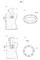
図4(a)、(b)に示すように、ウエハチャック30の吸着部31には、高さが固定された固定支持部材としてのピン36aと、それよりも高く設定されたゴム等の弾性材で形成された伸縮性の支持部材としてのリング32が設けられている。尚、図4(b)〜(d)までは、図4(a)の丸で囲んだ部分を拡大して示している。
【0052】
ウエハWが、例えば、内面側より外周側が上に反り上がった状態である場合を想定すると、ウエハWは図4(b)に示すように、当初、ウエハWの内面側が、リング32b、32c側(リング32c側への当接状況は図示省略)に当接するように支持される。リング32a側では、ウエハWの反りが大きいため、十分に吸引力が作用せず、ウエハWの裏面はリング32a上には当接していない。
【0053】
この状態で、図示しない真空ポンプ等の吸引手段に接続した吸引孔37で真空吸引を行う。真空吸引に伴い、ウエハWは、吸着部31側に引きつけられる。かかる引きつけに際して、ピン36aより高いリング32bにはウエハWとの接触圧である押圧力が働き、リング32の伸縮性に基づき縮まって、図4(c)に示すように、ウエハWが全体的にウエハチャック30の吸着部31側に近づいてくる。
【0054】
このようにしてウエハWが、ウエハチャック30側に近づくと、リング32a側とウエハWの反りが大きい外周縁側との間が狭まり、それまで十分な吸引力が作用しなかったウエハWの外周縁部が引きつけられることとなる。
【0055】
かかるウエハWの外周縁部の吸着に際しては、リング32aは、リング32bの場合と同様に、吸引されるにしたがって、リング32aに押圧力が働き、リング32aの伸縮性に基づき縮まる。
【0056】
ウエハチャック30は、始めは、伸縮性支持部としてのリング32がウエハWの反り状態に合わせた状態で支持しながら吸引吸着し、その後、ウエハWの吸着状態に合わせてウエハとの接触圧に応じて縮まることにより、ウエハWの反り状態に合わせながら吸引吸着をすることとなる。
【0057】
このようにして、ウエハWの吸引吸着によって、当初ピン36aより高い位置でウエハWを支持していたリング32a、32b、32cが次第に縮まる。しかし、ピン36aの高さまで縮んだ時点で、ピン36aが硬質材で形成された高さが変わらない固定支持部として形成されているため、これ以上吸着してウエハWを吸着部31側に引きつけようとしても、逆に、ピン36aにはウエハWを上方に押し上げるような抗力が発生して、図4(d)に示すように、反ったウエハWは、表面が平らに設定される。
【0058】
そのためウエハWのフォトレジスト面の平坦度が十分に確保され、前記説明の露光装置10を用いた精密露光に際して、ウエハW上の場所毎の焦点ずれが発生せず、精緻な露光が確保される。
【0059】
露光が終了した段階で、ウエハチャック30の真空吸引を解除し、ウエハWを現像処理に渡す。真空吸引を解除して、ウエハWが外されたウエハチャック30では、吸着時に縮んでいたリング32は、ウエハWによる押圧力がなくなるため上方に伸びて、図4(b)に示すように、ピン36aより高い元の位置に復帰した待機状態となり、次のウエハWの吸着を待つこととなる。
【0060】
現像処理されたフォトレジストは、エッチングマスクとして使用され、先に形成した成膜上にドライエッチングによる浅溝加工を施す。必要の都度、ステップS230に基づくフォトレジストの塗布、露光、現像を繰り返すことにより、Si3N4、SiO2、Si基板の順に必要な浅溝加工を施す。
【0061】
その後、エッチングマスクとして使用したフォトレジストは、アッシング処理により除去し、さらにSiO2膜を浅溝の深さより上になるように成膜し、CMP( Chemical Mechanical Polishing )処理により全体を平坦に研磨する。研磨は、Si3N4の表面がでる程度まで行い、リン酸液等を使用してウエットエッチングでこのSi3N4膜を除去して、平らな素子分離構造を形成する。
【0062】
このようにしてステップS230のフォトプロセスを繰り返し使用することにより、素子分離構造を形成した後、ウエル形成を行う。
【0063】
ウエル形成に際しては、例えば、3重ウエル形成を例に挙げて説明すれば、前記説明のステップS230のフォトプロセスに従い、フォトレジストを薄膜状に形成した上で、ウエハチャック30によりウエハWを吸着し、その状態で、露光装置10により精密露光を行い、その後現像処理にて深いnウエルのフォトレジストパターンを形成する。
【0064】
かかる深いnウエル形成用フォトレジストパターンをマスクとして、高エネルギーイオン注入により、リンイオン(P+)を打込み、所定範囲にn型不純物の導入を行う。
【0065】
同様にして、ステップS230のフォトプロセスを利用して、pウエル領域が開口されたフォトレジストパターンを形成し、これをマスクとしてホウ素イオン(B+)を打込み、p型不純物の導入を行う。併せて、浅いnウエル形成用フォトレジストパターンを、ステップS230に従い形成して、これをマスクとして、リンイオン(P+)を打込み、所定範囲に浅いウエルへのn型不純物の導入を行う。
【0066】
その後、フォトレジストをアッシングにより除去し、アニールを行って、イオン打込みにより導入した不純物の活性化を行えば、ウエル形成が終了する。ウエル形成後は、トランジスタの形成を行う。
【0067】
トランジスタの形成に際しては、例えば、熱酸化により薄いゲート酸化膜を形成する。かかるゲート酸化膜上に、PolySiとWSi2をCVD処理によりゲート電極膜として堆積する。
【0068】
かかるゲート電極膜上に、Si3N4等をCVD処理により成膜して、ゲートパターンの微細加工を行う。微細加工は、例えば、ステップS230のフォトプロセスを使用して、ゲート多層膜の連続ドライエッチングを行えばよい。
【0069】
その後、pMOS、nMOS領域を各々ステップS230を使用して開口しながら、ゲートパターンの両側に、ソース、ドレーンの不純物を浅く低濃度でイオン注入を行う。
【0070】
さらに、ゲートパターンを覆うようにSi3N4を成膜し、異方性ドライエッチングを行ってゲートの側壁部側にSi3N4を残し、その後、再度、ソース、ドレーンのイオン打込みを高濃度に行う。
【0071】
かかるトランジスタの形成後は、ビット線を形成する。層間SiO2をCVDで成膜後、CMPで平坦化処理を行い、コンタクト孔のフォトリソグラフィーをステップS230に沿って、前記説明の要領で行う。
【0072】
SiO2を選択エッチングしてコンタクト孔を形成した後、PolySiでコンタクト孔を充填し、ソース、ドレーンのプラグ(引き出し端子)を形成する。かかるプラグを形成後、SiO2を成膜して、ビット線形成部分のみ開口する。この開口部に、スパッタリングでW/TiNバリア膜を設けて、ビット線を形成する。
【0073】
ビット線の形成後は、キャパシタを形成する。すなわち、上記のように形成したビット線上に、PolySiプラグをキャパシタ形成位置に継ぎ足して形成する。その後、SiO2をキャパシタの高さに見合う膜厚でCVDにより成膜する。キャパシタの孔パターンをS230のフォトプロセスの前記説明の要領で形成し、これをマスクとしてエッチングする。
【0074】
その後、SiO2の孔の内面を含めて全面に薄いPolySi膜をCVDで形成し、表面のPolySi膜をエッチバックで除去することにより、キャパシタの下部電極としてのPolySi電極を形成する。その上に、Ta2O5絶縁膜、TiN膜をCVDで成膜することによりプレートと呼ばれる上部電極を設けて、キャパシタの形成を行う。
【0075】
このようにして、素子分離領域の形成、ウエルの形成、トランジスタの形成、ビット線の形成、キャパシタの形成を順次行うことにより、ステップS210の基板工程を終了する。ステップS210の基板工程終了後は、ステップS220の配線工程に移る。
【0076】
すなわち、キャパシタの形成後、層間絶縁膜を成膜する。かかる層間絶縁膜に、ステップS230のフォトプロセスを適用して、スルーホールパターンを形成する。このパターンをエッチングマスクとしてエッチング処理することによりコンタクト孔を形成する。その後、WやTiN埋め込みによりスルーホールプラグを形成する。
【0077】
さらに、Al/TiNの積層膜をスパッタリングで成膜し、ステップS230のフォトプロセスにより配線パターンを形成し、このパターンに基づいてエッチング処理して、Alの第1配線層を形成する。
【0078】
形成したAlの第1配線層上に、上記第1配線層を形成したと同様の要領で、Alの第2配線層を形成する。第2のAl配線層を形成した後に、保護膜を形成して、ウエハWへのDRAMの回路の作り込みを終了する。
【0079】
このようにして多数のDRAMの作り込みがなされたウエハは、ステップS300の組立工程に移される。組立工程では、ステップS310のダイシング工程で、多数のチップが形成されたウエハをウエハテープ上に載せ、その状態で例えば、チップ毎にハーフカットして、その後にウエハテープをエキスパンドすることにより、チップの個片化を行う。
【0080】
個片化された半導体チップは、ステップS320のボンディング工程で、例えば、チップマウンタ等を用いてリードフレーム上にダイボンディングされ、さらに半導体チップの電極とリードフレームのインナーリードとをワイヤボンディングする。
【0081】
ボンディング工程終了後は、ステップS330の封止工程で、ワイヤボンディング終了後の状態で樹脂封止して半導体チップの保護を行う。
【0082】
樹脂封止後は、ステップS340の仕上げ工程で、例えば、リードフレームのアウターリードにめっきを行い、さらにリード切断を行い、リードの曲げ加工を行う。かかる仕上げ処理の終了後、ステップS350のマーキング工程で、モールド部に製品番号などのマーキングを行って、半導体装置の組立が完成する。
【0083】
このように半導体装置の製造においては、基板工程、配線工程で、ステップS230によるフォトリソグラフィー工程が繰り返し使用されて、種々のパターン形成を行うが、かかる処理において、前記説明の露光装置10に装備されたウエハチャック30を用いて、焦点異常が発生しないようにウエハWを平坦に吸着保持して、精密露光が確実に行われる。
【0084】
上記説明のウエハチャック30を使用することにより、反りウエハを反り状態に合わせて確実に吸着し、さらに、吸着状態で平坦にウエハを保持することができる。
【0085】
尚、上記ウエハ処理工程の説明では、説明が煩瑣になるのを避けるため、処理の流れの主な部分についてのフォトリソグラフィーの使用状況のみを説明し、その他のフォトリソグラフィーの使用状況についてその説明を省略している。
【0086】
(実施の形態2)
前記実施の形態1では、リング32を、それ自体をゴム等の弾性材で形成することにより、伸縮性を持たせる構成を採用したが、リング32をピン36aと同様にセラミック等の硬質材で形成しておき、かかるリング32をばね等の伸縮部材を介在させて設ける構成でも、その伸縮性を確保することができる。
【0087】
例えば、図5(a)、(b)に示すように、セラミック等の硬質材で形成したリング32を、吸着部31に対してばね38a等の弾性部材38を介して設けるようにしても構わない。リング32にかかる押圧力に応じてばね38aが適宜伸縮するように構成しておけばよい。
【0088】
因みに、図5(a)に示す構成では、ばね38aは、図5(b)に示すように、短断面が略く字形状に折り曲げられ、全体がリング状の板ばねに形成されている。必要に応じて、ばね力の確保のために板面にスリットを入れておけばよい。
【0089】
図5(c)では、コイル状に形成したばね38bを用いて、リング32の伸縮性を確保する構成を示した。ばね38bは、図5(d)に示すように、リング32の取り付け範囲であるリング状の範囲39内に、所定間隔で、複数箇所均等に配置するようにすればよい。図5(d)では、8個のばね38bをリング状の範囲39に均等配置した構成を例示した。
【0090】
要は、リング32を上下に伸縮できるように構成できれば、上記方法以外の手段を採用しても構わない。
【0091】
(実施の形態3)
本実施の形態では、前記実施の形態1、2とは異なり、複数の吸着部がそれぞれ吸着位置の変更が行えるように構成して、ウエハの反りに合わせた吸着位置を確保した状態で、反りウエハの吸着が行えるようにした構成である。
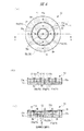
【0092】
本実施の形態で説明するウエハチャック50は、図6(a)に示すように、吸引吸着するウエハWに合わせた大きさの吸着部51が設けられている。吸着部51は、平面円形状の中央吸着部52と、中央吸着部52の周囲を同心リング状に囲むように設けられたリング状吸着部53とから構成されている。中央吸着部52、リング状吸着部53は、共に、セラミック等の材質で形成されている。
【0093】
リング状吸着部53は、最外周側に設けられた外側リング状吸着部53aと、その内側に設けられた内側リング状吸着部53bとから構成されている。図6(a)に示す場合には、内側リング状吸着部53bが1個設けられている場合を示しているが、必要に応じて、2個以上設けても構わない。
【0094】
中央吸着部52、リング状吸着部53は、共に、図6(b)に示すように、チャック台座54上に吸着側を上方に向けて設けられている。中央吸着部52は、略円柱状に形成され、底面側に伸縮部材55を介在させて、チャック台座54上に設けられている。伸縮部材55としては、例えば、ゴム等の弾性部材55a用いることができる。
【0095】
中央吸着部52の表面には、チャック台座54、伸縮部材55、セラミック製の中央吸着部52を貫通する吸引孔56の吸引開口部56aが設けられている。チャック台座54を貫通する吸引孔56は、図示はしないが、真空ポンプ等に接続されるようになっている。
【0096】
中央吸着部52の表面には、その周縁に沿って、図6(a)、(b)に示すように、外周リング57が突設されている。併せて、外周リング57に囲まれるようにして、中央吸着部52の表面には、多数の突設部58としてピン58aが設けられている。ピン58aと、外周リング57は、その高さが一致させられている。
【0097】
尚、図6(b)の断面図では、見やすいように、ピン58aの図示は省略している。以下、ウエハチャックの断面図では、特に示す場合を除いては、図6(b)同様に、ピン58aの図示を省略している。
【0098】
中央吸着部52を同心状に囲んで、内側リング状吸着部53aが、チャック台座54上に、伸縮部材55を介在させて設けられている。伸縮部材55としては、例えば、ゴム等の弾性部材55bを用いることができる。
【0099】
内側リング状吸着部53aの表面には、チャック台座54、伸縮部材55、およびセラミック製の内側リング状吸着部53aを貫通して吸引孔56の吸引開口部56aが設けられている。チャック台座54を貫通する吸引孔56は、図示はしないが、真空ポンプ等に接続されるようになっている。
【0100】
内側リング状吸着部53bの周縁には、その外周縁、内周縁の両方に、外周リング57、内周リング59が設けられている。外周リング57、内周リング59の双方に囲まれた内側リング状吸着部53bの表面には、複数のピン58aが突設部58として設けられている。ピン58aと、外周リング57、内周リング59は、その高さが一致させられている。
【0101】
内側リング状吸着部53bを同心リング状に囲むように、外側リング状吸着部53aが、図6に示すように設けられている。セラミック製の外側リング状吸着部53aは、伸縮部材55を介在させることなく、チャック台座54に設けられている。
【0102】
外側リング状吸着部53aの表面には、チャック台座54およびセラミック製の外側リング状吸着部53aを貫通して吸引孔56の吸引開口部56aが設けられている。チャック台座54を貫通する吸引孔56は、図示はしないが、真空ポンプ等に接続されるようになっている。
【0103】
外側リング状吸着部53aの周縁には、その外周縁、内周縁の両方に、外周リング57、内周リング59が設けられている。外周リング57、内周リング59の双方に囲まれた外側リング状吸着部53aの表面には、複数のピン58aが突設部58として設けられている。ピン58aと、外周リング57、内周リング59は、その高さが一致させられている。
【0104】
内側リンク状吸着部53bは、上記構成の中央吸着部52の周囲に、弾性部材55a、55bの伸縮度合いに応じて、互いに独立して上下動ができるように設けられている。かかる上下動により、吸着位置の高さ調整が行える。
【0105】
一方、外側リング状吸着部53aは、内側リング状吸着53b、中央吸着部52とは異なり、伸縮部材55を介在させてチャック台座54に設けられていないため、吸着位置の高さ変更は行えない。
【0106】
かかる構成のウエハチャック50では、図6(c)に示すように、内面側が低く外周面側に向けて高く反った反りウエハWの吸着に際しては、ウエハWの裏面の中央側の低い反りに対応した中央吸着部52では、伸縮部材55aが縮んで吸着位置を一番低くした状態になってウエハWを吸着している。
【0107】
併せて、ウエハW裏面の中央側の低い部分をリング状に囲む中間部分に対応して、内側リング状吸着部53bでは、伸縮部材55の弾性部材55bが少し縮んだ状態で、中央吸着部52より少し高い吸着位置に調節されて、ウエハWを吸着している。
【0108】
併せて、ウエハW裏面の外周側の高い部分は、吸着位置の高さが固定された外側リング状吸着部53aに吸着されている。
【0109】
このように、本発明の図6に示すウエハチャック50を使用することにより、ウエハWの反りに合わせて、複数の吸着部の吸着位置の高さが異なるように調節されて、吸引吸着が行われることとなる。すなわち、ウエハWの反りを残した状態で吸引吸着することができる。
【0110】
かかる反りを残した状態で吸着することができるので、ウエハ径が大きく、小さいウエハ径の場合とは異なり、反り矯正を行うと割れが発生する虞がある場合でも、かかる割れの心配なくウエハ吸着を行うことができる。
【0111】
図7に示すように、吸着部が固定され、吸着位置の高さ変更が行えない構成のウエハチャック60とは異なり、反りウエハWに合わせて吸着位置の変更を行って、反りウエハを確実に吸着することができる。
【0112】
因みに、図7に示す構成のウエハチャック60では、吸着部は円盤状に形成され、その外周縁に沿って、外周リング57が設けられ、さらに、同心リング状に、2個の内周リング59a、59bが設けられている。
【0113】
内周リング59bに囲まれた中央吸着部61、内周リング59a、59bに囲まれたリング状吸着部62、外周リング57、内周リング59aにより囲まれたリング状吸着部63は、一体に形成され、各々の表面には、突設部58としてピン58aが複数設けられたピンコンタクト型の構成を有している。
【0114】
また、中央吸着部61、リンク状吸着部62、63は、上記説明の本発明のウエハチャック50とは異なり、それぞれの吸着部が互いに独立して上下に吸着位置の高さが変えられるようには構成されていない。
【0115】
かかる構成のウエハチャック60では、図7(b)に示すように、ウエハWの反りが小さい場合には、ウエハWの外周縁では、リング状吸着部63側との距離がそれ程離れてはおらず、吸引孔56真空吸引により比較的安定して吸引されることとなる。
【0116】
しかし、図7(c)に示すように、ウエハWの反りが大きい場合には、ウエハWの外周縁では、リング状吸着部63側との距離が大きく離れることとなり、吸引孔56の真空吸引では十分に吸着させることができない。
【0117】
これに反して、上記説明の本実施の形態のウエハチャック50では、図6(c)に示すように、ウエハWの反りが大きい場合でも、ウエハWの内側面に対応したリング状吸着部53b、中央吸着部52が、順次、外側リング状吸着部53aより相対的に低い吸着位置となることにより、ウエハWの外周縁では、外側リング状吸着部53aとの距離が大きく離れずに済み、吸引孔56の真空吸引で十分に吸着させることができる。反りが150μmを超えるような大きな場合でも、十分に真空吸着でウエハのチャックを行うことができる。
【0118】
(実施の形態4)
本実施の形態では、前記実施の形態3で説明した構成の伸縮部材55の代わりに、ピエゾ素子64を用いた構成を有している。その他の構成は、図6に示す構成と同様である。
【0119】
本実施の形態のウエハチャック70では、図8(a)の断面図に示すように、中央吸着部52、リング状吸着部53(53a、53b)が同心リング状に、チャック台座54上に設けられている。中央吸着部52、リング状吸着部53bは、共に、伸縮部材としてピエゾ素子64a(64)64b(64)を介在させてチャック台座54に設けられている。
【0120】
各ピエゾ素子64a、64bは、外部からの電気信号により体積変化を起こして、伸縮を行うこととなる。その結果、各ピエゾ素子64a、64bを介在させてチャック台座54に設けた中央吸着部52、リング状吸着部53bは、上下に伸縮できるように構成されている。
【0121】
かかる構成のウエハチャック70は、次のようにして使用する。すなわち、図9(a)に例示した制御系のブロック図に示すように、ウエハチャック70に吸引吸着するウエハWの反りを、ウエハチャック70に吸着させる前に、光歪み計等の反り測定装置71を使用して、中央吸着部52、リング状吸着部53a、53bに対応した反り状況を測定しておく。
【0122】
測定に際しては、例えば、リング状吸着部53aに対応した側を基準として、その他の反りレベルをその基準からの高さとして測定すればよい。かかる測定結果を、電気信号等で反り情報として変換装置72に送る。変換装置72では、送られてきた反り情報に応じて、どの程度吸着位置の調整を行えばよいか演算して、その位置調整に必要な各ピエゾ素子64a、64bの変位量に見合う電気量を算出し、制御信号をウエハチャック70の各ピエゾ素子64a、64bに送る。
【0123】
各ピエゾ素子64a、64bは、各々に送られた制御信号に基づき、電流調整がなされて体積変化を行い、例えば、図8(b)に示すように、ウエハの反り状況に合わせて各吸着部の吸着位置の高さを調節する。
【0124】
すなわち、リング状吸着部53bの吸着位置を、リング状吸着部53aより低い位置に調整し、併せて、中央吸着部52の吸着位置をリング状吸着部53bよりさらに低く、一番に低くして、リング状吸着部53a、53b、中央吸着部52からなる吸着部全体の吸着位置をウエハWの反りに合わせた状態に調整する。
【0125】
この状態で、ウエハWをウエハチャック70上に載せて、吸引孔56から真空吸引を行って吸着を始める。吸着は、予めウエハWの反りに合わせて吸引位置に調整が行われているため、反った状態でもウエハWの吸着を確実に行うことができる。
【0126】
このようにして、ウエハWを反った状態で吸着した後で、各ピエゾ素子64a、64bに対して、電気信号を送って、リング状吸着部53b、中央吸着部52の吸着位置の高さが、吸着位置が固定されたリング状吸着部53aのレベルに復帰するまでピエゾ素子64a、64bの体積増加を行わせる。かかる復帰工程により、反った状態で当初吸引吸着されていたウエハWは、リング状吸着部53b、中央吸着部52が持ち上げられ、一旦は反り状態に合わせて吸着されたウエハWが、反りが解消された状態の平らな状態で吸着されることとなる。すなわち、反りが矯正されることとなる。
【0127】
かかる本実施の形態のウエハチャック70では、前記実施の形態1、2と同様に、吸着時のウエハWを平坦な状態にすることができるので、焦点深度の短い露光光を使用する精密露光装置のウエハチャックとして極めて有効に使用することができる。
【0128】
また、図9(b)には、図9(a)と異なる制御系を示す。かかる制御系では、当初から、図8(a)に示す状態で反りウエハWを吸着し始める。ウエハWの反り状況に合わせて、中央吸着部52、リング状吸着部53a、53bの接触圧をピエゾ素子の電気変化として捉えて、リアルタイムに反り情報を制御装置73に送る。
【0129】
制御装置73では、送られた各吸着部の電気変化から、各吸着部の電気変化がリング状吸着部53aの電気変化に等しくなるように、各ピエゾ素子64a、64bに制御信号を送って体積変化を起こさせて、ウエハWの反りに合わせた状態に吸着位置の調整を行って、ウエハWを反った状態で一旦確実に吸着する。
【0130】
ウエハWを確実に吸着した後は、制御装置73から制御信号を送って、各ピエゾ素子64a、64bに対して、リング状吸着部53b、中央吸着部52の吸着位置の高さが、吸着位置が固定されたリング状吸着部53aのレベルに復帰するまでピエゾ素子64a、64bの体積増加を行わせて、ウエハWの吸着状態を平坦になるように行い、吸着後のウエハWの反りを矯正する。
【0131】
以上、本発明者によってなされた発明を実施の形態に基づき具体的に説明したが、本発明は前記実施の形態に限定されるものではなく、その要旨を逸脱しない範囲で種々変更可能であることはいうまでもない。
【0132】
例えば、前記実施の形態では、吸着部に通じる吸引孔を個々の吸着部に各別に設けて、各々の吸引孔を真空ポンプに接続する構成を示したが、個々の吸引孔を共通のチャンバに繋ぎ、このチャンバを真空ポンプに繋ぐ構成を採用しても構わない。適宜、現場に合わせた構成を選択すればよい。
【0133】
例えば、上記説明では、露光装置にウエハチャックを組み込んだ場合を例に挙げて説明したが、露光装置以外にも、ウエハ搬送アームのウエハ載置部に、あるいは、スピンコート法等に用いるウエハの吸着回転部に、研磨工程におけるウエハ保持部等に使用することもできる。
【0134】
さらには、半導体ウエハの、ガラス基板等の表面欠陥を光により検査する場合に、ウエハ等の被保持体を平坦に保持する必要があるチャック部に使用することができる。要は、ウエハ等の被保持体を真空吸着で保持するチャック部であれば、上記例示以外の構成でも適用することができる。
【0135】
また、前記説明では、メモリ半導体としてDRAMを半導体装置の一例として挙げて説明したが、これ以外のメモリ半導体でも、ロジックICでも、光半導体等の半導体装置にも適用できることは言うまでもない。
【0136】
【発明の効果】
本願によって開示される発明のうち、代表的なものによって得られる効果を簡単に説明すれば、以下の通りである。
【0137】
すなわち、ウエハの反り状態に合わせてウエハの吸着を行うことができる。
【図面の簡単な説明】
【図1】本発明のウエハチャックを組み込んだ露光装置の構成例を模式的に示す説明図である。
【図2】(a)は、本発明に係るウエハチャックの一実施例を示す平面図であり、(b)は(a)で示すA−A線で切断した場合を模式的に示す断面図である。
【図3】半導体装置の一実施例の製造方法を示すフロー図である。
【図4】(a)、(b)、(c)、(d)は、図2に示すウエハチャックによる反りウエハの吸着過程を示す要部断面説明図である。
【図5】(a)は図2に示す構成のウエハチャックのリングの伸縮機構の変形例を示す要部断面説明図、(b)は(a)の斜視図であり、(c)は(a)とは異なる伸縮機構の別の変形例を示す要部断面説明図であり、(d)は(c)の要部平面図である。
【図6】(a)は、吸着部が個々独立に吸着位置の高さ変更ができるように構成した本発明に係るウエハチャックの一実施例の平面図であり、(b)、(c)は、ウエハの吸着過程を(a)のA−A線で切断した断面状況で示す要部断面説明図である。
【図7】(a)は、吸着位置の高さ変更ができないこれまでのウエハチャックの一実施例の平面図であり、(b)、(c)は、ウエハの吸着過程を(a)のA−A線で切断した断面状況で示す要部断面説明図である。
【図8】(a)は、ピエゾ素子を用いた構成の本発明に係るウエハチャックを示す要部断面図であり、(b)、(c)はウエハの吸着過程を示す断面説明図である。
【図9】(a)、(b)は、図8に示す構成のピエゾ素子の制御系を模式的に示すブロック図である。
【符号の説明】
10 露光装置
10a 走査型縮小投影露光装置
11 露光光源
12 フライアイレンズ
13 アパーチャ
14 コンデンサレンズ
15 コンデンサレンズ
16 ミラー
17 マスク
18 ペリクル
19 投影レンズ
21 マスク位置制御手段
22 ミラー
23 ステージ
30 ウエハチャック
31 吸着部
32 リング
32a リング
32b リング
32c リング
33 中央吸着部
34 リング状吸着部
35 リング状吸着部
36 固定支持部
36a ピン
37 吸引孔
37a 吸引孔開口部
38 弾性部材
38a ばね
38b ばね
39 範囲
41 Zステージ
41a 駆動手段
42 XYステージ
42a 駆動手段
43 主制御系
44 ミラー
45 レーザ測長機
50 ウエハチャック
51 吸着部
52 中央吸着部
53 リング状吸着部
53a 外側リング状吸着部
53b 内側リング状吸着部
54 チャック台座
55 伸縮部材
55a 弾性部材
55b 弾性部材
56 吸引孔
56a 吸引孔開口部
57 外周リング
58 突設部
58a ピン
59 内周リング
60 ウエハチャック
61 中央吸着部
62 リング状吸着部
63 リング状吸着部
64 ピエゾ素子
64a ピエゾ素子
64b ピエゾ素子
70 ウエハチャック
71 反り測定装置
72 変換装置
73 制御装置
Lp 露光光
W ウエハ[0001]
TECHNICAL FIELD OF THE INVENTION
The present invention relates to a semiconductor device manufacturing technique, and more particularly to a technique effective when applied to a wafer holding mechanism in a semiconductor device manufacturing process.
[0002]
[Prior art]
The technology described below has been studied by the inventor when researching and completing the present invention, and the outline thereof is as follows.
[0003]
In the manufacture of a semiconductor device, various processes are performed on the surface of a wafer to form a circuit by stacking a large number of insulating layers, wiring layers, and the like. In the processing of such a wafer surface, it is required to hold the wafer surface at a correct position in the processing direction.
[0004]
As a wafer holding mechanism, a configuration is generally known in which a wafer is vacuum-sucked by a device called a chuck or a wafer chuck.
[0005]
When the wafer is sucked, the presence of foreign matter between the wafer surface to be sucked and the suction surface must be avoided in order to secure the flatness of the wafer surface during the suction. Therefore, in order to minimize the contact area of the back surface of the wafer at the time of suction from the viewpoint of preventing such foreign matter from intervening, a so-called pin contact system is used in which the back surface of the wafer is not supported by the surface but supported by a large number of pins. Was suggested.
[0006]
The vacuum chuck type wafer chuck adopting the pin contact method has a disk-shaped chuck main body whose surface is approximately adjusted to the wafer diameter, and a ring-shaped side wall called an outer peripheral ring is protruded from a peripheral edge of the main body surface. I have.
[0007]
On the surface of the main body inside the outer peripheral ring, a suction opening connected to a suction hole for suctioning the back surface of the wafer and a number of pins for supporting the back surface of the wafer are provided in a protruding manner. The suction hole is configured to be connected to a vacuum pump or the like through a hollow portion inside the chuck body.
[0008]
By vacuum-suctioning through the suction hole with the front surface of the wafer chuck body facing the back surface of the wafer, the back surface of the wafer is attracted to the front surface of the chuck body. At the time of suction, the back surface of the wafer is supported by the outer peripheral ring set at a predetermined height and the tips of a number of pins.
[0009]
On the other hand, semiconductor devices are formed by making various circuits on the front side of a thin silicon wafer to form fine circuits. The structure is more multilayered. Therefore, the wafer is more likely to be warped than before.
[0010]
However, since the device configuration of the wafer chuck is basically based on the premise that the wafer is flat, there is a case where sufficient suction cannot be performed when there is a warped wafer.
[0011]
For example, in the case of a wafer whose inner surface side is low and its outer edge side is high and warped upward, the outer edge side of the wafer is not sufficiently attracted to the wafer chuck.
[0012]
Therefore, as a configuration for adsorbing such a warped wafer, a notch is provided in the outer peripheral ring of the wafer chuck corresponding to the outer edge side of the wafer, and gas is drawn into the inside of the wafer chuck at a high speed from the notch at the time of suction. A configuration has been proposed in which the outer edge side of the wafer is sucked by the effect (for example, see Patent Document 1).
[0013]
[Patent Document 1]
JP-A-8-37227 (FIGS. 2 and 4)
[0014]
[Problems to be solved by the invention]
However, the present inventor has found that the above-mentioned vacuum chuck type wafer chuck technology has the following problems.
[0015]
In other words, according to the wafer chuck having the configuration using the Venturi effect, even a warped wafer that cannot be suctioned by the conventional wafer chuck can be sufficiently suctioned, and the wafer surface can be suctioned flatly. Technology.
[0016]
However, in the above configuration, since the wafer supporting height of the wafer chuck is fixed to the same height, the amount of warpage is large, and the wafer chuck does not function effectively for a warped wafer that does not sufficiently act on the Venturi effect. It is also possible.
[0017]
For example, when the warpage is large, that is, when the value indicated by the difference between the lower part and the higher part of the wafer surface exceeds 150 μm, the outer edge side shows an extremely higher warp than the center side, and at the time of suction, the outer peripheral part of the wafer On the side, there is a case where a large gap is formed between the chuck and the chuck, so that air leaks and vacuum suction becomes difficult.
[0018]
In addition, regarding the warpage of the wafer, assuming that the current mainstream warpage of a φ200 mm wafer is carried over to a φ300 mm wafer that is expected to shift in the future, the wafer surface becomes lower due to the increase in the wafer diameter. The value indicated by the difference between the high point and the high point is further expanded from the current level, and it is expected that it becomes more difficult to attract the warped wafer than the current level.
[0019]
Under such circumstances, it can be said that the technique of suctioning the warped wafer is becoming more important. Therefore, the present inventor thought that if the suction can be performed in accordance with the warp state of the wafer, such a problem can be solved.
[0020]
SUMMARY OF THE INVENTION It is an object of the present invention to enable a vacuum chuck to chuck a wafer according to the warpage of the wafer.
[0021]
The above and other objects and novel features of the present invention will become apparent from the description of the present specification and the accompanying drawings.
[0022]
[Means for Solving the Problems]
The following is a brief description of an outline of typical inventions disclosed in the present application.
[0023]
That is, in the present invention, the suction is performed in a state in which the wafer is warped.
[0024]
BEST MODE FOR CARRYING OUT THE INVENTION
Hereinafter, embodiments of the present invention will be described in detail with reference to the drawings. In all the drawings for describing the embodiments, members having the same functions are denoted by the same reference numerals, and repeated description thereof may be omitted.
[0025]
(Embodiment 1)
FIG. 1 is an explanatory diagram showing a schematic configuration of an exposure apparatus incorporating a wafer chuck according to one embodiment of the present invention. FIG. 2A is a plan view showing an embodiment of the wafer chuck, and FIG. 2B is a sectional view.
[0026]
FIG. 1 shows only those parts necessary for explaining the function of the exposure apparatus. The other portions required for the exposure apparatus (scanner or stepper) of the normal configuration are not particularly described to avoid complicated description, but are provided in the exposure apparatus shown in FIG. 1 similarly to the normal configuration. Things.
[0027]
As shown in FIG. 1, the
[0028]
Light emitted from the exposure light source 11 illuminates the
[0029]
The
[0030]
As the exposure light Lp, for example, a KrF excimer laser light having an exposure wavelength of about 248 nm can be used. Exposure can be performed under the condition that the numerical aperture NA of the optical lens is 0.65, the illumination shape is circular, and the coherency (σ: sigma) value is 0.7.
[0031]
The exposure light Lp is not limited to the above, but can be variously changed. For example, g-line, i-line, ArF excimer laser light (wavelength 193 nm) or F 2 (Fluorine) excimer laser light (wavelength 157 nm) can also be used.
[0032]
The wafer W is vacuum-sucked on the
[0033]
The
[0034]
In addition, the surface position of the wafer W is measured by a focus position detection unit included in a normal exposure apparatus. By driving the
[0035]
The
[0036]
The
[0037]
The
[0038]
The
[0039]
The height of the
[0040]
The
[0041]
Further, as shown in FIGS. 2A and 2B, the suction surface of each of the
[0042]
On the other hand, unlike the
[0043]
FIG. 2B is a cross-sectional view of FIG. 2A taken along the line AA. In FIG. 2B, the illustration of the
[0044]
The height of the
[0045]
A method of manufacturing a semiconductor device by incorporating the
[0046]
As shown in the manufacturing flow of FIG. 3, in step S100, a predetermined wafer (silicon wafer) is supplied. A desired circuit is formed by performing various processes on the supplied wafer in a wafer processing step of step S200. Such circuit formation is performed in the substrate process in step S210 and the wiring process in step S220. In each of the steps, the photo process S230 is performed by the above-described
[0047]
In the substrate process of
[0048]
The wafer supplied in step S100 is first cleaned, and then, the surface of the wafer is 2 Of a thin film of Si 3 N 4 Laminate the films.
[0049]
Next, the process proceeds to the photo process S230. A photoresist liquid of a photosensitive resin is dropped on the wafer W on which the film is formed, and the wafer is rotated at a high speed in the dropped state to form a thin photoresist film.
[0050]
In this state, the wafer W is sucked and held by the
[0051]
As shown in FIGS. 4A and 4B, the
[0052]
Assuming that the wafer W is, for example, in a state in which the outer peripheral side is warped upward from the inner surface side, as shown in FIG. 4B, the inner surface side of the wafer W is initially set to the
[0053]
In this state, vacuum suction is performed through a
[0054]
When the wafer W approaches the
[0055]
When the outer peripheral edge of the wafer W is attracted, the
[0056]
At first, the
[0057]
In this manner, the
[0058]
Therefore, the flatness of the photoresist surface of the wafer W is sufficiently ensured, and during precise exposure using the
[0059]
When the exposure is completed, the vacuum suction of the
[0060]
The developed photoresist is used as an etching mask, and shallow groove processing by dry etching is performed on the previously formed film. By repeating the application, exposure and development of the photoresist based on step S230 whenever necessary, 3 N 4 , SiO 2 Then, necessary shallow groove processing is performed in the order of the Si substrate.
[0061]
Thereafter, the photoresist used as an etching mask is removed by ashing, and furthermore,
[0062]
By repeatedly using the photo process of step S230 in this way, a well is formed after an element isolation structure is formed.
[0063]
At the time of forming the well, for example, if a triple well formation is described as an example, a photoresist is formed in a thin film shape according to the photo process of step S230 described above, and then the wafer W is sucked by the
[0064]
Using such a deep n-well forming photoresist pattern as a mask, phosphorus ions (P + ) Is implanted to introduce an n-type impurity into a predetermined range.
[0065]
Similarly, a photoresist pattern having an opening in the p-well region is formed by using the photo process of step S230, and using this as a mask, boron ions (B + ) Is implanted to introduce p-type impurities. At the same time, a shallow n-well forming photoresist pattern is formed in accordance with step S230, and the + ) Is implanted to introduce an n-type impurity into a shallow well within a predetermined range.
[0066]
Thereafter, the photoresist is removed by ashing, annealing is performed, and the impurity introduced by ion implantation is activated, thereby completing the well formation. After the formation of the well, a transistor is formed.
[0067]
In forming the transistor, a thin gate oxide film is formed by, for example, thermal oxidation. PolySi and WSi are formed on the gate oxide film. 2 Is deposited as a gate electrode film by a CVD process.
[0068]
On such a gate electrode film, Si 3 N 4 And the like are formed by a CVD process, and fine processing of the gate pattern is performed. For the fine processing, for example, continuous dry etching of the gate multilayer film may be performed using the photo process of step S230.
[0069]
Thereafter, while the pMOS and nMOS regions are opened using step S230, the source and drain impurities are ion-implanted on both sides of the gate pattern at a shallow and low concentration.
[0070]
Further, Si is so covered as to cover the gate pattern. 3 N 4 And anisotropic dry etching is performed to form Si on the side wall of the gate. 3 N 4 After that, ion implantation of the source and drain is performed again at a high concentration.
[0071]
After forming such a transistor, a bit line is formed. Interlayer SiO 2 Is formed by CVD, planarization is performed by CMP, and photolithography of the contact hole is performed in step S230 as described above.
[0072]
SiO 2 Is selectively etched to form a contact hole, and then the contact hole is filled with PolySi to form plugs (lead terminals) for source and drain. After forming such a plug, the SiO 2 Is formed, and only the bit line forming portion is opened. A W / TiN barrier film is provided in the opening by sputtering to form a bit line.
[0073]
After the formation of the bit line, a capacitor is formed. That is, a PolySi plug is formed on the bit line formed as described above by adding it to the capacitor forming position. After that, the SiO 2 Is formed by CVD with a film thickness corresponding to the height of the capacitor. The hole pattern of the capacitor is formed in the manner described in the photo process of S230, and etching is performed using this as a mask.
[0074]
After that, the SiO 2 A thin PolySi film is formed on the entire surface including the inner surface of the hole by CVD, and the PolySi film on the surface is removed by etch back to form a PolySi electrode as a lower electrode of the capacitor. On top of that, Ta 2 O 5 By forming an insulating film and a TiN film by CVD, an upper electrode called a plate is provided to form a capacitor.
[0075]
In this manner, the formation of the element isolation region, the formation of the well, the formation of the transistor, the formation of the bit line, and the formation of the capacitor are sequentially performed, thereby completing the substrate process in step S210. After the completion of the substrate process in step S210, the process proceeds to a wiring process in step S220.
[0076]
That is, after forming the capacitor, an interlayer insulating film is formed. By applying the photo process of step S230 to the interlayer insulating film, a through-hole pattern is formed. A contact hole is formed by performing an etching process using this pattern as an etching mask. After that, a through-hole plug is formed by embedding W or TiN.
[0077]
Further, a laminated film of Al / TiN is formed by sputtering, a wiring pattern is formed by a photo process in step S230, and etching is performed based on the pattern to form a first wiring layer of Al.
[0078]
A second wiring layer of Al is formed on the formed first wiring layer of Al in the same manner as the formation of the first wiring layer. After forming the second Al wiring layer, a protective film is formed, and the fabrication of the DRAM circuit on the wafer W is completed.
[0079]
The wafer on which a large number of DRAMs have been formed in this manner is transferred to the assembly process of step S300. In the assembling process, in the dicing process of step S310, a wafer on which a large number of chips are formed is placed on a wafer tape, and in that state, for example, half-cut is performed for each chip, and then the wafer tape is expanded. Is singulated.
[0080]
The singulated semiconductor chip is die-bonded to the lead frame using, for example, a chip mounter or the like in the bonding step of step S320, and furthermore, the electrodes of the semiconductor chip and the inner leads of the lead frame are wire-bonded.
[0081]
After the completion of the bonding step, in a sealing step of step S330, the semiconductor chip is protected by resin sealing in a state after the completion of the wire bonding.
[0082]
After the resin sealing, in the finishing step of step S340, for example, the outer leads of the lead frame are plated, and the leads are further cut and bent. After the completion of the finishing process, in the marking step of step S350, marking such as a product number is performed on the mold portion, and the assembly of the semiconductor device is completed.
[0083]
As described above, in the manufacture of the semiconductor device, in the substrate process and the wiring process, the photolithography process in step S230 is repeatedly used to form various patterns. Using the
[0084]
By using the
[0085]
In the above description of the wafer processing step, in order to avoid the description from being complicated, only the usage of photolithography for the main part of the processing flow will be described, and the usage of other photolithography will be described. Omitted.
[0086]
(Embodiment 2)
In the first embodiment, the
[0087]
For example, as shown in FIGS. 5A and 5B, a
[0088]
Incidentally, in the configuration shown in FIG. 5A, the
[0089]
FIG. 5C illustrates a configuration in which the elasticity of the
[0090]
In short, any means other than the above method may be adopted as long as the
[0091]
(Embodiment 3)
In the present embodiment, unlike the first and second embodiments, a plurality of suction units are configured to be able to change the suction position, and the warpage is secured in a state where the suction position is adjusted to the warpage of the wafer. The configuration is such that the wafer can be sucked.
[0092]
As shown in FIG. 6A, a
[0093]
The ring-shaped
[0094]
As shown in FIG. 6B, both the
[0095]
On the surface of the
[0096]
As shown in FIGS. 6A and 6B, an outer
[0097]
In the sectional view of FIG. 6B, the
[0098]
An inner ring-shaped
[0099]
A
[0100]
An outer
[0101]
An outer ring-shaped
[0102]
On the surface of the outer ring-shaped
[0103]
An
[0104]
The inner link-shaped
[0105]
On the other hand, unlike the inner ring-shaped
[0106]
In the
[0107]
At the same time, in the inner ring-shaped
[0108]
At the same time, a high portion on the outer peripheral side of the back surface of the wafer W is sucked by the outer ring-shaped
[0109]
As described above, by using the
[0110]
Since the wafer can be suctioned with such a warp remaining, unlike the case where the wafer diameter is large and the wafer diameter is small, even if the warp correction may cause a crack, the wafer suction can be performed without worrying about such a crack. It can be performed.
[0111]
As shown in FIG. 7, unlike the
[0112]
Incidentally, in the
[0113]
The
[0114]
Also, unlike the above-described
[0115]
In the
[0116]
However, as shown in FIG. 7C, when the warp of the wafer W is large, the outer peripheral edge of the wafer W is largely apart from the ring-shaped
[0117]
On the other hand, in the above-described
[0118]
(Embodiment 4)
In the present embodiment, a configuration using a piezo element 64 is used instead of the
[0119]
In the
[0120]
Each of the
[0121]
The
[0122]
In the measurement, for example, the other warpage level may be measured as a height from the reference with the side corresponding to the ring-shaped
[0123]
Each of the
[0124]
That is, the suction position of the ring-shaped
[0125]
In this state, the wafer W is placed on the
[0126]
In this way, after the wafer W is sucked in a warped state, an electric signal is sent to each of the
[0127]
In the
[0128]
FIG. 9B shows a control system different from that of FIG. 9A. In this control system, the warped wafer W starts to be sucked from the beginning in the state shown in FIG. In accordance with the warp state of the wafer W, the contact pressure between the
[0129]
The
[0130]
After the wafer W is surely sucked, a control signal is sent from the
[0131]
As described above, the invention made by the inventor has been specifically described based on the embodiment. However, the present invention is not limited to the embodiment, and various modifications can be made without departing from the gist of the invention. Needless to say.
[0132]
For example, in the above-described embodiment, a configuration has been described in which suction holes communicating with the suction units are separately provided in the individual suction units, and the suction holes are connected to the vacuum pump, but the individual suction holes are connected to a common chamber. A configuration in which the chamber is connected to a vacuum pump may be employed. The configuration may be appropriately selected according to the site.
[0133]
For example, in the above description, the case where the wafer chuck is incorporated in the exposure apparatus has been described as an example. However, in addition to the exposure apparatus, the wafer mounting part of the wafer transfer arm, or the wafer used for the spin coating method or the like may be used. It can also be used as a suction holding unit, a wafer holding unit in a polishing process, or the like.
[0134]
Further, when inspecting a surface defect of a semiconductor wafer, such as a glass substrate, by light, the semiconductor wafer can be used for a chuck portion that needs to hold an object such as a wafer flat. In short, any configuration other than the above example can be applied as long as it is a chuck unit that holds a held body such as a wafer by vacuum suction.
[0135]
In the above description, a DRAM has been described as an example of a semiconductor device as a memory semiconductor, but it goes without saying that the present invention can be applied to other semiconductor devices such as a memory semiconductor, a logic IC, and an optical semiconductor.
[0136]
【The invention's effect】
The effects obtained by typical aspects of the invention disclosed in the present application will be briefly described as follows.
[0137]
That is, the wafer can be suctioned according to the warped state of the wafer.
[Brief description of the drawings]
FIG. 1 is an explanatory view schematically showing a configuration example of an exposure apparatus incorporating a wafer chuck of the present invention.
FIG. 2A is a plan view showing one embodiment of a wafer chuck according to the present invention, and FIG. 2B is a cross-sectional view schematically showing a case cut along line AA shown in FIG. It is.
FIG. 3 is a flowchart illustrating a method for manufacturing a semiconductor device according to an embodiment;
4 (a), (b), (c) and (d) are cross-sectional views of a main part showing a process of sucking a warped wafer by a wafer chuck shown in FIG. 2;
5 (a) is a cross-sectional view of a principal part showing a modification of the expansion / contraction mechanism of the ring of the wafer chuck having the configuration shown in FIG. 2, (b) is a perspective view of (a), and (c) is ( It is principal part sectional drawing which shows another modification of the expansion-contraction mechanism different from a), and (d) is a principal part top view of (c).
FIG. 6A is a plan view of an embodiment of the wafer chuck according to the present invention, in which the suction unit is configured to be able to independently change the height of the suction position, and FIGS. 6B and 6C. FIG. 4 is an explanatory sectional view of a main part, showing a wafer suction process in a sectional state taken along line AA in FIG.
FIG. 7A is a plan view of one embodiment of a conventional wafer chuck in which the height of a suction position cannot be changed, and FIGS. 7B and 7C illustrate a wafer suction process in FIG. It is principal part sectional explanatory drawing shown in the cross-sectional state cut | disconnected by the AA line.
8A is a cross-sectional view of a main part showing a wafer chuck according to the present invention having a configuration using a piezo element, and FIGS. 8B and 8C are cross-sectional explanatory views showing a wafer suction process. .
FIGS. 9A and 9B are block diagrams schematically showing a control system of the piezo element having the configuration shown in FIG. 8;
[Explanation of symbols]
10 Exposure equipment
10a Scanning reduction projection exposure apparatus
11 Exposure light source
12 Fly Eye Lens
13 Aperture
14 Condenser lens
15 Condenser lens
16 mirror
17 Mask
18 Pellicle
19 Projection lens
21 Mask position control means
22 mirror
23 stages
30 Wafer chuck
31 Suction unit
32 rings
32a ring
32b ring
32c ring
33 Central suction unit
34 Ring-shaped suction unit
35 Ring-shaped suction unit
36 fixed support
36a pin
37 suction hole
37a Suction hole opening
38 Elastic member
38a spring
38b spring
39 range
41 Z Stage
41a driving means
42 XY stage
42a driving means
43 Main control system
44 mirror
45 Laser measuring machine
50 Wafer chuck
51 Suction unit
52 Central suction part
53 Ring-shaped suction unit
53a Outer ring-shaped suction part
53b Inner ring-shaped suction part
54 chuck base
55 telescopic members
55a elastic member
55b elastic member
56 suction holes
56a Suction hole opening
57 Outer ring
58 Projection
58a pin
59 Inner circumference ring
60 Wafer chuck
61 Central suction part
62 Ring-shaped suction part
63 Ring-shaped suction unit
64 piezo elements
64a piezo element
64b piezo element
70 Wafer chuck
71 Warpage measuring device
72 Converter
73 Controller
Lp exposure light
W wafer
Claims (5)
前記ウエハの吸着を、前記ウエハの反りに合わせて行うことを特徴とする半導体装置の製造方法。A method of manufacturing a semiconductor device, which has an operation of holding a wafer by suction and suction during a manufacturing process,
A method of manufacturing a semiconductor device, wherein the wafer is attracted in accordance with the warpage of the wafer.
反りのある前記ウエハを、前記反りを残した状態で吸着し、吸着後、吸着状態を維持しながら前記ウエハの反りを矯正することを特徴とする半導体装置の製造方法。A method of manufacturing a semiconductor device, which has an operation of holding a wafer by suction and suction during a manufacturing process,
A method of manufacturing a semiconductor device, comprising: adsorbing a warped wafer while the warpage remains, and correcting the warp of the wafer while maintaining the suction state after the suction.
前記ウエハチャックは、独立して吸着位置の高さ変更を行う複数の吸着部を有することを特徴とする半導体装置の製造方法。A method for manufacturing a semiconductor device, which includes an operation of holding a wafer by suctioning and sucking the wafer by a wafer chuck during a manufacturing process,
The method of manufacturing a semiconductor device, wherein the wafer chuck has a plurality of suction units that independently change the height of a suction position.
前記ウエハチャックは、中央吸着部と、前記中央吸着部を囲むように設けたリング状吸着部とを有し、
前記リング状吸着部の内、最外周に位置する外側リング状吸着部の吸着位置の高さは固定され、
前記外側リング状吸着部より内側に位置する内側リング状吸着部と前記中央吸着部とは、上下方向に伸縮する伸縮部材を介して設けられ、
前記ウエハの反りに合わせて、前記内側リング状吸着部と前記中央吸着部の吸着位置の高さが変わることを特徴とする半導体装置の製造方法。A method for manufacturing a semiconductor device, which includes an operation of holding a wafer by suctioning and sucking the wafer by a wafer chuck during a manufacturing process,
The wafer chuck has a center suction unit and a ring-shaped suction unit provided so as to surround the center suction unit,
Of the ring-shaped suction portions, the height of the suction position of the outer ring-shaped suction portion located at the outermost periphery is fixed,
The inner ring-shaped suction portion and the center suction portion located on the inner side of the outer ring-shaped suction portion are provided via an elastic member that expands and contracts in a vertical direction,
A method of manufacturing a semiconductor device, wherein the height of the suction positions of the inner ring-shaped suction portion and the central suction portion changes in accordance with the warpage of the wafer.
前記ウエハチャックは、ウエハ吸着時の前記ウエハとの接触圧に応じて支持高さを変更する伸縮性支持部と、
前記ウエハの支持高さが固定された固定支持部とを有し、
前記伸縮性支持部は、前記固定支持部より、ウエハ吸着前の待機状態で高く設定されていることを特徴とする半導体装置の製造方法。A method for manufacturing a semiconductor device, which includes an operation of holding a wafer by suctioning and sucking the wafer by a wafer chuck during a manufacturing process,
The wafer chuck has a stretchable supporting portion that changes a supporting height in accordance with a contact pressure with the wafer during wafer suction,
A fixed support portion in which the support height of the wafer is fixed,
The method of manufacturing a semiconductor device, wherein the elastic supporting portion is set higher than the fixed supporting portion in a standby state before wafer suction.
Priority Applications (1)
| Application Number | Priority Date | Filing Date | Title |
|---|---|---|---|
| JP2003016904A JP2004228453A (en) | 2003-01-27 | 2003-01-27 | Method of manufacturing semiconductor device |
Applications Claiming Priority (1)
| Application Number | Priority Date | Filing Date | Title |
|---|---|---|---|
| JP2003016904A JP2004228453A (en) | 2003-01-27 | 2003-01-27 | Method of manufacturing semiconductor device |
Publications (1)
| Publication Number | Publication Date |
|---|---|
| JP2004228453A true JP2004228453A (en) | 2004-08-12 |
Family
ID=32904193
Family Applications (1)
| Application Number | Title | Priority Date | Filing Date |
|---|---|---|---|
| JP2003016904A Pending JP2004228453A (en) | 2003-01-27 | 2003-01-27 | Method of manufacturing semiconductor device |
Country Status (1)
| Country | Link |
|---|---|
| JP (1) | JP2004228453A (en) |
Cited By (17)
| Publication number | Priority date | Publication date | Assignee | Title |
|---|---|---|---|---|
| JP2006116454A (en) * | 2004-10-22 | 2006-05-11 | Seiko Epson Corp | Slit coat type coater and slit coat type application method |
| JP2006269867A (en) * | 2005-03-25 | 2006-10-05 | Canon Inc | Exposure apparatus |
| JP2008108766A (en) * | 2006-10-23 | 2008-05-08 | Toppan Printing Co Ltd | Chuck and spin coating device |
| JP2012099787A (en) * | 2010-10-07 | 2012-05-24 | Tokyo Electron Ltd | Heat treatment apparatus and heat treatment method |
| JP2015027715A (en) * | 2013-07-30 | 2015-02-12 | 富士通株式会社 | Hand holder |
| JP2015106711A (en) * | 2013-11-29 | 2015-06-08 | エルジー ディスプレイ カンパニー リミテッド | Substrate separating device |
| KR20160143816A (en) * | 2014-05-06 | 2016-12-14 | 에이에스엠엘 네델란즈 비.브이. | Substrate support, method for loading a substrate on a substrate support location, lithographic apparatus and device manufacturing method |
| WO2017086333A1 (en) * | 2015-11-19 | 2017-05-26 | 日本特殊陶業株式会社 | Vacuum chuck |
| JP2017112343A (en) * | 2015-12-18 | 2017-06-22 | 日本特殊陶業株式会社 | Substrate holding device and substrate holding method |
| JP2017162987A (en) * | 2016-03-09 | 2017-09-14 | 日本特殊陶業株式会社 | Vacuum sucking member and vacuum sucking method |
| JP2017220483A (en) * | 2016-06-03 | 2017-12-14 | 日本特殊陶業株式会社 | Vacuum chuck and manufacturing method of vacuum chuck |
| JP2018533763A (en) * | 2015-10-29 | 2018-11-15 | エーエスエムエル ネザーランズ ビー.ブイ. | Substrate table for lithographic apparatus and method of loading a substrate |
| EP3385792A3 (en) * | 2018-04-26 | 2018-12-26 | ASML Netherlands B.V. | Stage apparatus for use in a lithographic apparatus |
| JP2019114590A (en) * | 2017-12-21 | 2019-07-11 | 日本特殊陶業株式会社 | Vacuum suction member |
| CN110556327A (en) * | 2018-05-30 | 2019-12-10 | 台湾积体电路制造股份有限公司 | Wafer suction cup |
| JP2020064930A (en) * | 2018-10-16 | 2020-04-23 | 株式会社ディスコ | Wafer holding device and processing method of wafer using wafer holding device |
| US11243476B2 (en) | 2018-04-26 | 2022-02-08 | Asml Netherlands B.V. | Stage apparatus, lithographic apparatus, control unit and method |
-
2003
- 2003-01-27 JP JP2003016904A patent/JP2004228453A/en active Pending
Cited By (40)
| Publication number | Priority date | Publication date | Assignee | Title |
|---|---|---|---|---|
| JP2006116454A (en) * | 2004-10-22 | 2006-05-11 | Seiko Epson Corp | Slit coat type coater and slit coat type application method |
| JP4513960B2 (en) * | 2004-10-22 | 2010-07-28 | セイコーエプソン株式会社 | Slit coat type coating apparatus and slit coat type coating method |
| JP2006269867A (en) * | 2005-03-25 | 2006-10-05 | Canon Inc | Exposure apparatus |
| JP2008108766A (en) * | 2006-10-23 | 2008-05-08 | Toppan Printing Co Ltd | Chuck and spin coating device |
| JP2012099787A (en) * | 2010-10-07 | 2012-05-24 | Tokyo Electron Ltd | Heat treatment apparatus and heat treatment method |
| JP2015027715A (en) * | 2013-07-30 | 2015-02-12 | 富士通株式会社 | Hand holder |
| JP2015106711A (en) * | 2013-11-29 | 2015-06-08 | エルジー ディスプレイ カンパニー リミテッド | Substrate separating device |
| KR20160143816A (en) * | 2014-05-06 | 2016-12-14 | 에이에스엠엘 네델란즈 비.브이. | Substrate support, method for loading a substrate on a substrate support location, lithographic apparatus and device manufacturing method |
| CN106255924A (en) * | 2014-05-06 | 2016-12-21 | Asml荷兰有限公司 | Substrate holder, for loading the method for substrate, lithographic equipment and device making method on substrate supports position |
| US10656536B2 (en) | 2014-05-06 | 2020-05-19 | Asml Netherlands B.V. | Substrate support, method for loading a substrate on a substrate support location, lithographic apparatus and device manufacturing method |
| JP2017515148A (en) * | 2014-05-06 | 2017-06-08 | エーエスエムエル ネザーランズ ビー.ブイ. | Substrate support, method for mounting a substrate on a substrate support location, lithographic apparatus, and device manufacturing method |
| JP2019144599A (en) * | 2014-05-06 | 2019-08-29 | エーエスエムエル ネザーランズ ビー.ブイ. | Substrate supporter, method for mounting substrate on substrate supporter location, lithography device, and device manufacturing method |
| KR101932208B1 (en) * | 2014-05-06 | 2018-12-24 | 에이에스엠엘 네델란즈 비.브이. | Substrate support, method for loading a substrate on a substrate support location, lithographic apparatus and device manufacturing method |
| JP2018533763A (en) * | 2015-10-29 | 2018-11-15 | エーエスエムエル ネザーランズ ビー.ブイ. | Substrate table for lithographic apparatus and method of loading a substrate |
| JP2022010193A (en) * | 2015-10-29 | 2022-01-14 | エーエスエムエル ネザーランズ ビー.ブイ. | Substrate table for lithographic apparatus and method of loading substrate |
| JP2020118983A (en) * | 2015-10-29 | 2020-08-06 | エーエスエムエル ネザーランズ ビー.ブイ. | Substrate table for lithographic apparatus and method of loading substrate |
| CN107408530A (en) * | 2015-11-19 | 2017-11-28 | 日本特殊陶业株式会社 | Vacuum chuck |
| WO2017086333A1 (en) * | 2015-11-19 | 2017-05-26 | 日本特殊陶業株式会社 | Vacuum chuck |
| JPWO2017086333A1 (en) * | 2015-11-19 | 2017-11-16 | 日本特殊陶業株式会社 | Vacuum chuck |
| JP2017112343A (en) * | 2015-12-18 | 2017-06-22 | 日本特殊陶業株式会社 | Substrate holding device and substrate holding method |
| KR102071149B1 (en) * | 2016-03-09 | 2020-01-29 | 니혼도꾸슈도교 가부시키가이샤 | Vacuum suction member and vacuum suction method |
| WO2017154436A1 (en) * | 2016-03-09 | 2017-09-14 | 日本特殊陶業株式会社 | Vacuum suction member and vacuum suction method |
| JP2017162987A (en) * | 2016-03-09 | 2017-09-14 | 日本特殊陶業株式会社 | Vacuum sucking member and vacuum sucking method |
| TWI636500B (en) * | 2016-03-09 | 2018-09-21 | 日本特殊陶業股份有限公司 | Vacuum adsorption method |
| US11279005B2 (en) | 2016-03-09 | 2022-03-22 | Ngk Spark Plug Co., Ltd. | Vacuum suction member and vacuum suction method |
| KR20180035786A (en) * | 2016-03-09 | 2018-04-06 | 니혼도꾸슈도교 가부시키가이샤 | Vacuum suction member and vacuum suction method |
| CN107851604A (en) * | 2016-03-09 | 2018-03-27 | 日本特殊陶业株式会社 | Vacuum suction component and vacuum suction method |
| CN107851604B (en) * | 2016-03-09 | 2021-11-12 | 日本特殊陶业株式会社 | Vacuum adsorption member and vacuum adsorption method |
| JP2017220483A (en) * | 2016-06-03 | 2017-12-14 | 日本特殊陶業株式会社 | Vacuum chuck and manufacturing method of vacuum chuck |
| JP2019114590A (en) * | 2017-12-21 | 2019-07-11 | 日本特殊陶業株式会社 | Vacuum suction member |
| JP7014590B2 (en) | 2017-12-21 | 2022-02-01 | 日本特殊陶業株式会社 | Vacuum suction member |
| EP3385792A3 (en) * | 2018-04-26 | 2018-12-26 | ASML Netherlands B.V. | Stage apparatus for use in a lithographic apparatus |
| US11243476B2 (en) | 2018-04-26 | 2022-02-08 | Asml Netherlands B.V. | Stage apparatus, lithographic apparatus, control unit and method |
| CN110556327A (en) * | 2018-05-30 | 2019-12-10 | 台湾积体电路制造股份有限公司 | Wafer suction cup |
| US11201079B2 (en) | 2018-05-30 | 2021-12-14 | Taiwan Semiconductor Manufacturing Company, Ltd. | Wafer chuck |
| TWI732152B (en) * | 2018-05-30 | 2021-07-01 | 台灣積體電路製造股份有限公司 | Wafer chuck |
| CN110556327B (en) * | 2018-05-30 | 2022-11-29 | 台湾积体电路制造股份有限公司 | Wafer suction cup |
| CN111063646A (en) * | 2018-10-16 | 2020-04-24 | 株式会社迪思科 | Wafer holding device and wafer processing method using the same |
| JP2020064930A (en) * | 2018-10-16 | 2020-04-23 | 株式会社ディスコ | Wafer holding device and processing method of wafer using wafer holding device |
| JP7208759B2 (en) | 2018-10-16 | 2023-01-19 | 株式会社ディスコ | Wafer processing method using wafer holding device |
Similar Documents
| Publication | Publication Date | Title |
|---|---|---|
| JP2004228453A (en) | Method of manufacturing semiconductor device | |
| US7385835B2 (en) | Membrane 3D IC fabrication | |
| KR100804006B1 (en) | Wafer chuck, exposure system, and method of manufacturing semiconductor device | |
| US7176545B2 (en) | Apparatus and methods for maskless pattern generation | |
| US7494830B2 (en) | Method and device for wafer backside alignment overlay accuracy | |
| US7463334B2 (en) | Exposure apparatus and device manufacturing method | |
| JPH10233433A (en) | Substrate supporting device and aligner using the device as well as manufacturing method of device | |
| KR100550755B1 (en) | Substrate holding device | |
| JP2007184342A (en) | Exposure system, exposure method and device manufacturing method | |
| JP2001127145A (en) | Method and device for holding substrate with suction and exposing device and device manufacturing method using the device | |
| KR20190035443A (en) | Wafer table with dynamic support pins | |
| JP4411158B2 (en) | Exposure equipment | |
| JP5933289B2 (en) | SOI wafer and manufacturing method thereof | |
| JP2004221296A (en) | Substrate holding device and aligner, and device manufacturing method | |
| TWI570873B (en) | Semiconductor structure and manufacturing method for the same | |
| JP4342202B2 (en) | Method of forming alignment mark and method of manufacturing semiconductor device using the same | |
| JP2003007678A (en) | Semiconductor device and manufacturing method therefor | |
| JP2023119554A (en) | Substrate holding device, substrate holding method, lithography device, and manufacturing method for article | |
| JPH1154398A (en) | Aligner, exposure method, and manufacture of semiconductor integrated circuit device using the same | |
| JPH11260682A (en) | Formation of alignment mark and manufacture of semiconductor device | |
| JP2000188249A (en) | Aligner and manufacture of device | |
| KR20060074969A (en) | Manufacturing method for semiconductor device | |
| KR20000045385A (en) | Method for manufacturing semiconductor device | |
| KR20060094189A (en) | Equipment for aligning wafer |
Legal Events
| Date | Code | Title | Description |
|---|---|---|---|
| A621 | Written request for application examination |
Free format text: JAPANESE INTERMEDIATE CODE: A621 Effective date: 20051219 |
|
| A977 | Report on retrieval |
Free format text: JAPANESE INTERMEDIATE CODE: A971007 Effective date: 20080814 |
|
| A131 | Notification of reasons for refusal |
Free format text: JAPANESE INTERMEDIATE CODE: A131 Effective date: 20080916 |
|
| A02 | Decision of refusal |
Free format text: JAPANESE INTERMEDIATE CODE: A02 Effective date: 20090324 |