JP2004207323A - Semiconductor composite device - Google Patents
Semiconductor composite device Download PDFInfo
- Publication number
- JP2004207323A JP2004207323A JP2002371724A JP2002371724A JP2004207323A JP 2004207323 A JP2004207323 A JP 2004207323A JP 2002371724 A JP2002371724 A JP 2002371724A JP 2002371724 A JP2002371724 A JP 2002371724A JP 2004207323 A JP2004207323 A JP 2004207323A
- Authority
- JP
- Japan
- Prior art keywords
- semiconductor
- led
- region
- film
- layer
- Prior art date
- Legal status (The legal status is an assumption and is not a legal conclusion. Google has not performed a legal analysis and makes no representation as to the accuracy of the status listed.)
- Granted
Links
- 239000004065 semiconductor Substances 0.000 title claims abstract description 108
- 239000002131 composite material Substances 0.000 title claims abstract description 96
- 239000010410 layer Substances 0.000 claims abstract description 220
- 239000000758 substrate Substances 0.000 claims abstract description 81
- 239000011229 interlayer Substances 0.000 claims abstract description 15
- 239000010408 film Substances 0.000 claims description 168
- 239000010409 thin film Substances 0.000 claims description 42
- 238000000034 method Methods 0.000 claims description 23
- 230000002093 peripheral effect Effects 0.000 claims description 5
- 150000001875 compounds Chemical class 0.000 claims description 2
- 229910052751 metal Inorganic materials 0.000 abstract description 46
- 239000002184 metal Substances 0.000 abstract description 46
- 239000000463 material Substances 0.000 abstract description 17
- 229910001218 Gallium arsenide Inorganic materials 0.000 description 21
- 238000005530 etching Methods 0.000 description 16
- 238000004519 manufacturing process Methods 0.000 description 14
- 238000009792 diffusion process Methods 0.000 description 13
- 239000010931 gold Substances 0.000 description 13
- KDLHZDBZIXYQEI-UHFFFAOYSA-N Palladium Chemical compound [Pd] KDLHZDBZIXYQEI-UHFFFAOYSA-N 0.000 description 10
- 239000011701 zinc Substances 0.000 description 9
- 229910000980 Aluminium gallium arsenide Inorganic materials 0.000 description 8
- PCHJSUWPFVWCPO-UHFFFAOYSA-N gold Chemical compound [Au] PCHJSUWPFVWCPO-UHFFFAOYSA-N 0.000 description 8
- 229910052737 gold Inorganic materials 0.000 description 8
- PXHVJJICTQNCMI-UHFFFAOYSA-N Nickel Chemical compound [Ni] PXHVJJICTQNCMI-UHFFFAOYSA-N 0.000 description 5
- 239000004820 Pressure-sensitive adhesive Substances 0.000 description 5
- 238000005253 cladding Methods 0.000 description 5
- 230000004048 modification Effects 0.000 description 5
- 238000012986 modification Methods 0.000 description 5
- MHAJPDPJQMAIIY-UHFFFAOYSA-N Hydrogen peroxide Chemical compound OO MHAJPDPJQMAIIY-UHFFFAOYSA-N 0.000 description 4
- NBIIXXVUZAFLBC-UHFFFAOYSA-N Phosphoric acid Chemical compound OP(O)(O)=O NBIIXXVUZAFLBC-UHFFFAOYSA-N 0.000 description 4
- 229910052763 palladium Inorganic materials 0.000 description 4
- 238000000206 photolithography Methods 0.000 description 4
- 229910021420 polycrystalline silicon Inorganic materials 0.000 description 4
- 229920005591 polysilicon Polymers 0.000 description 4
- 239000002356 single layer Substances 0.000 description 4
- KRHYYFGTRYWZRS-UHFFFAOYSA-N Fluorane Chemical compound F KRHYYFGTRYWZRS-UHFFFAOYSA-N 0.000 description 3
- 229910052782 aluminium Inorganic materials 0.000 description 3
- XAGFODPZIPBFFR-UHFFFAOYSA-N aluminium Chemical compound [Al] XAGFODPZIPBFFR-UHFFFAOYSA-N 0.000 description 3
- 239000004020 conductor Substances 0.000 description 3
- 230000007547 defect Effects 0.000 description 3
- 229910000040 hydrogen fluoride Inorganic materials 0.000 description 3
- 239000000203 mixture Substances 0.000 description 3
- BASFCYQUMIYNBI-UHFFFAOYSA-N platinum Chemical compound [Pt] BASFCYQUMIYNBI-UHFFFAOYSA-N 0.000 description 3
- 229920001721 polyimide Polymers 0.000 description 3
- 239000000126 substance Substances 0.000 description 3
- 239000004642 Polyimide Substances 0.000 description 2
- XUIMIQQOPSSXEZ-UHFFFAOYSA-N Silicon Chemical compound [Si] XUIMIQQOPSSXEZ-UHFFFAOYSA-N 0.000 description 2
- 239000000853 adhesive Substances 0.000 description 2
- 230000001070 adhesive effect Effects 0.000 description 2
- 229910000147 aluminium phosphate Inorganic materials 0.000 description 2
- 230000015572 biosynthetic process Effects 0.000 description 2
- 238000005229 chemical vapour deposition Methods 0.000 description 2
- 125000005842 heteroatom Chemical group 0.000 description 2
- 239000012535 impurity Substances 0.000 description 2
- 238000001451 molecular beam epitaxy Methods 0.000 description 2
- 229910052759 nickel Inorganic materials 0.000 description 2
- 229910052710 silicon Inorganic materials 0.000 description 2
- 239000010703 silicon Substances 0.000 description 2
- 229910000679 solder Inorganic materials 0.000 description 2
- 239000007790 solid phase Substances 0.000 description 2
- 239000010936 titanium Substances 0.000 description 2
- 238000009281 ultraviolet germicidal irradiation Methods 0.000 description 2
- 229910002704 AlGaN Inorganic materials 0.000 description 1
- 229910004298 SiO 2 Inorganic materials 0.000 description 1
- RTAQQCXQSZGOHL-UHFFFAOYSA-N Titanium Chemical compound [Ti] RTAQQCXQSZGOHL-UHFFFAOYSA-N 0.000 description 1
- HCHKCACWOHOZIP-UHFFFAOYSA-N Zinc Chemical compound [Zn] HCHKCACWOHOZIP-UHFFFAOYSA-N 0.000 description 1
- 229910021417 amorphous silicon Inorganic materials 0.000 description 1
- 239000000969 carrier Substances 0.000 description 1
- 238000006243 chemical reaction Methods 0.000 description 1
- 230000000694 effects Effects 0.000 description 1
- 229910052732 germanium Inorganic materials 0.000 description 1
- GNPVGFCGXDBREM-UHFFFAOYSA-N germanium atom Chemical compound [Ge] GNPVGFCGXDBREM-UHFFFAOYSA-N 0.000 description 1
- 239000011810 insulating material Substances 0.000 description 1
- 238000002488 metal-organic chemical vapour deposition Methods 0.000 description 1
- 229910021421 monocrystalline silicon Inorganic materials 0.000 description 1
- 150000004767 nitrides Chemical class 0.000 description 1
- 230000003287 optical effect Effects 0.000 description 1
- 229910052697 platinum Inorganic materials 0.000 description 1
- 238000005498 polishing Methods 0.000 description 1
- JBQYATWDVHIOAR-UHFFFAOYSA-N tellanylidenegermanium Chemical compound [Te]=[Ge] JBQYATWDVHIOAR-UHFFFAOYSA-N 0.000 description 1
- 229910052719 titanium Inorganic materials 0.000 description 1
- 238000005406 washing Methods 0.000 description 1
- XLYOFNOQVPJJNP-UHFFFAOYSA-N water Substances O XLYOFNOQVPJJNP-UHFFFAOYSA-N 0.000 description 1
- 229910052725 zinc Inorganic materials 0.000 description 1
Images


Classifications
-
- H—ELECTRICITY
- H01—ELECTRIC ELEMENTS
- H01L—SEMICONDUCTOR DEVICES NOT COVERED BY CLASS H10
- H01L25/00—Assemblies consisting of a plurality of individual semiconductor or other solid state devices ; Multistep manufacturing processes thereof
- H01L25/16—Assemblies consisting of a plurality of individual semiconductor or other solid state devices ; Multistep manufacturing processes thereof the devices being of types provided for in two or more different main groups of groups H01L27/00 - H01L33/00, or in a single subclass of H10K, H10N, e.g. forming hybrid circuits
- H01L25/167—Assemblies consisting of a plurality of individual semiconductor or other solid state devices ; Multistep manufacturing processes thereof the devices being of types provided for in two or more different main groups of groups H01L27/00 - H01L33/00, or in a single subclass of H10K, H10N, e.g. forming hybrid circuits comprising optoelectronic devices, e.g. LED, photodiodes
-
- B—PERFORMING OPERATIONS; TRANSPORTING
- B41—PRINTING; LINING MACHINES; TYPEWRITERS; STAMPS
- B41J—TYPEWRITERS; SELECTIVE PRINTING MECHANISMS, i.e. MECHANISMS PRINTING OTHERWISE THAN FROM A FORME; CORRECTION OF TYPOGRAPHICAL ERRORS
- B41J2/00—Typewriters or selective printing mechanisms characterised by the printing or marking process for which they are designed
- B41J2/435—Typewriters or selective printing mechanisms characterised by the printing or marking process for which they are designed characterised by selective application of radiation to a printing material or impression-transfer material
- B41J2/447—Typewriters or selective printing mechanisms characterised by the printing or marking process for which they are designed characterised by selective application of radiation to a printing material or impression-transfer material using arrays of radiation sources
- B41J2/45—Typewriters or selective printing mechanisms characterised by the printing or marking process for which they are designed characterised by selective application of radiation to a printing material or impression-transfer material using arrays of radiation sources using light-emitting diode [LED] or laser arrays
-
- H—ELECTRICITY
- H01—ELECTRIC ELEMENTS
- H01L—SEMICONDUCTOR DEVICES NOT COVERED BY CLASS H10
- H01L27/00—Devices consisting of a plurality of semiconductor or other solid-state components formed in or on a common substrate
- H01L27/15—Devices consisting of a plurality of semiconductor or other solid-state components formed in or on a common substrate including semiconductor components with at least one potential-jump barrier or surface barrier specially adapted for light emission
- H01L27/153—Devices consisting of a plurality of semiconductor or other solid-state components formed in or on a common substrate including semiconductor components with at least one potential-jump barrier or surface barrier specially adapted for light emission in a repetitive configuration, e.g. LED bars
-
- H—ELECTRICITY
- H01—ELECTRIC ELEMENTS
- H01L—SEMICONDUCTOR DEVICES NOT COVERED BY CLASS H10
- H01L2924/00—Indexing scheme for arrangements or methods for connecting or disconnecting semiconductor or solid-state bodies as covered by H01L24/00
- H01L2924/0001—Technical content checked by a classifier
- H01L2924/0002—Not covered by any one of groups H01L24/00, H01L24/00 and H01L2224/00
-
- H—ELECTRICITY
- H01—ELECTRIC ELEMENTS
- H01L—SEMICONDUCTOR DEVICES NOT COVERED BY CLASS H10
- H01L33/00—Semiconductor devices with at least one potential-jump barrier or surface barrier specially adapted for light emission; Processes or apparatus specially adapted for the manufacture or treatment thereof or of parts thereof; Details thereof
- H01L33/48—Semiconductor devices with at least one potential-jump barrier or surface barrier specially adapted for light emission; Processes or apparatus specially adapted for the manufacture or treatment thereof or of parts thereof; Details thereof characterised by the semiconductor body packages
- H01L33/62—Arrangements for conducting electric current to or from the semiconductor body, e.g. lead-frames, wire-bonds or solder balls
Abstract
Description
【0001】
【発明の属する技術分野】
本発明は、例えば、電子写真式プリンタに使用されるLEDプリントヘッドのような半導体複合装置に関する。
【0002】
【従来の技術】
図25は、従来のLEDプリントヘッドの一部を概略的に示す斜視図であり、図26は、図25のLEDプリントヘッドに備えることができるLEDアレイチップの一例を示す平面図である。図示されたLEDプリントヘッド900は、基板901上に備えられたLEDアレイチップ902の電極パッド903と、基板901上に備えられた駆動ICチップ904の電極パッド905とをボンディングワイヤ906で接続した構造を持つ。
【0003】
また、下記の特許文献1には、薄膜構造の発光素子が開示されている。
【0004】
【特許文献1】
特開平10−063807号公報(図3から図6まで、図8、段落0021)
【0005】
【発明が解決しようとする課題】
しかしながら、図25及び図26に示されたLEDプリントヘッド900では、LEDアレイチップ902と駆動ICチップ904とをボンディングワイヤ906によって接続していたので、LEDアレイチップ902と駆動ICチップ904のそれぞれにワイヤボンド用の大きな(例えば、100μm×100μm)電極パッド903及び905を設ける必要があった。このため、LEDアレイチップ902及び駆動ICチップ904の面積を小さくすることが困難であり、その結果、材料コストを削減することが困難であった。
【0006】
また、LEDアレイチップ902において発光部907として機能する領域は、表面から5μm程度の深さの領域である。しかし、図25及び図26に示されたLEDプリントヘッド900では、安定したワイヤボンドの歩留まりを確保するために、LEDアレイチップ902の厚さは駆動ICチップ904の厚さ(例えば、250μm〜300μm)と同程度にする必要があった。このため、LEDプリントヘッド900においては、LEDアレイチップ902の材料コストを削減することが困難であった。
【0007】
さらにまた、特許文献1には、薄膜構造の発光素子が開示されているが、発光素子にはハンダボール用の電極パッドが備えられており、この電極パッドにハンダボールを介して個別電極が接続されている。このように、特許文献1の薄膜構造の発光素子は電極パッドを備えているので、その面積を縮小することが困難であった。
【0008】
そこで、本発明は上記したような従来技術の課題を解決するためになされたものであり、その目的とするところは、小型化及び材料コストの低減を図ることができる半導体複合装置を提供することにある。
【0009】
【課題を解決するための手段】
本発明に係る半導体複合装置は、集積回路を有する半導体基板と、前記半導体基板の表面に形成された平坦化領域と、半導体素子を有し、前記平坦化領域上に貼り付けられた半導体薄膜とを備えたことを特徴としている。
【0010】
また、本発明に係る他の半導体複合装置は、集積回路を有する半導体基板と、前記半導体基板の前記集積回路が形成された領域に隣接する領域上に形成され、前記集積回路が形成された領域よりも高い位置に表面を持つかさあげ層と、前記かさあげ層の表面上に貼り付けられた半導体薄膜とを備えたことを特徴としている。
【0011】
また、本発明に係るさらに他の半導体複合装置は、集積回路を有する半導体基板と、前記半導体基板上に貼り付けられた半導体薄膜とを有し、前記半導体薄膜が、前記半導体素子が形成された側の第1の面を前記半導体基板側にしたことを特徴としている。
【0012】
【発明の実施の形態】
<第1の実施形態>
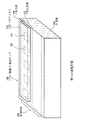
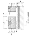
図1は、本発明の第1の実施形態に係る半導体複合装置であるLED/駆動IC複合チップの一部を概略的に示す斜視図であり、図2は、LEDエピフィルムのボンディング前におけるLED/駆動IC複合チップを概略的に示す斜視図である。また、図3は、LED/駆動IC複合チップの一部を概略的に示す平面図であり、図4は、図3をS4−S4線で切る面を概略的に示す断面図である。
【0013】
図1から図4までに示されるように、第1の実施形態に係るLED/駆動IC複合チップ100は、集積回路102を有する半導体基板であるシリコン(Si)基板101と、このSi基板101の表面に形成された平坦化領域103とを備えている。平坦化領域103は、Si基板101の表面上に絶縁膜(図示せず)を形成し、この絶縁膜が形成された面を平坦化処理(例えば、CMP(Chemical Mechanical Polishing)処理)した領域である。第1の実施形態において、平坦化領域103は、Si基板101の集積回路102上に形成されているが、Si基板101上の集積回路102に隣接する領域に形成してもよい。
【0014】
また、図1から図4までに示されるように、第1の実施形態に係るLED/駆動IC複合チップ100は、平坦化領域103上に形成された平坦化膜104を備えている。平坦化膜104は、メタル層105と、このメタル層105の周辺領域に形成された層間絶縁膜106とを有する。平坦化膜104の表面は、平坦化処理(例えば、CMP処理)されている。
【0015】
さらに、図1から図4までに示されるように、LED/駆動IC複合チップ100は、LED105を含み、平坦化膜104上に貼り付けられた(ボンディングされた)シート状の半導体エピタキシャルフィルム110(以下「LEDエピフィルム」と言う。)を備えている。なお、平坦化膜104を備えずに、LEDエピフィルム110をSi基板101の平坦化領域103の表面に直接貼り付けることもできる。
【0016】
LEDエピフィルム110には、複数のLED(発光部)120が形成されている。複数のLED120は、等ピッチで1列に配列されている。ただし、複数のLED120の配列は等ピッチに限定されない。また、複数のLED120の列数も1列に限定されず、例えば、複数のLED120の配列を、配列方向に直交する方向に規則的にずらしてもよい。また、LEDエピフィルム110に形成されるLED120の数は図示の個数に限定されない。また、図3に示されるように、LEDエピフィルム110は、LED120の発光領域の幅W2よりも広い幅W1を持つ。例えば、LED120の発光領域の幅W2を20μmとし、LEDエピフィルム110の幅W1を50μmとし、LED120の発光領域の両側にそれぞれ15μmの余裕を持たせている。LEDエピフィルム110の幅W1は、電極パッドを有する従来のLEDプリントヘッドの基板の幅(通常、400μm程度)よりも非常に小さい幅である。ただし、LEDエピフィルム110の幅W1及びLED120の発光領域の幅W2は上記した値に限定されない。
【0017】
LEDエピフィルム110は、後述するエピタキシャル層のみで構成されることが望ましい。LEDエピフィルム110の厚さは、LEDの安定した特性(例えば、発光特性や電気特性)を確保するために十分な厚さである2μm程度とすることができる。このLEDエピフィルム110の厚さは、電極パッドを有する従来のLEDプリントヘッドの厚さ(通常、300μm程度)よりも非常に薄い厚さである。また、LEDエピフィルム110の厚さが厚くなると、その上に形成される薄膜の配線層に段切れが発生する確率が高くなる。このような不良の発生を回避するためには、LEDエピフィルム110の厚さを、約10μm以下にすることが望ましい。ただし、ポリイミド等の絶縁体材料を使って、段差領域を平坦化する等の方策を講ずることによって、LEDエピフィルム110の厚さを10μmを超える厚さにすることもできる。
【0018】
Si基板101は、集積回路102が作り込まれたモノリシックSi基板である。Si基板101の集積回路102には、LEDエピフィルム110に形成された複数のLED120を駆動させるための複数の駆動ICが含まれる。ただし、集積回路102には、複数の駆動ICの他に、LED120の点灯制御に共通に使用される回路も含まれる。Si基板101の厚さは、例えば、約300μmである。集積回路102の表面は、層間絶縁膜の開口部、配線パターン、又はエッチングパターン等により凹凸を有する。この凹凸を有する集積回路102上に絶縁膜(図示せず)を形成し、平坦化処理(例えば、CMP処理)を施された領域が平坦化領域103である。
【0019】
平坦化膜104は、LEDエピフィルム110の発光部120が接着される予定の領域に形成された複数のメタル層105と、メタル層105が形成された領域の周辺領域にメタル層105と同じ厚さで形成された層間絶縁膜106とを含む。ただし、平坦化膜104の構造や材質は、図示のものに限定されない。平坦化膜104の構造や材質は、Si基板101の平坦化領域103の構造や材質、又は、LEDエピフィルム110の形状、大きさ、厚さ、材質等の各種要因に基づいて決定すればよい。
【0020】
図5(a)及び(b)は、平坦化膜104の形成プロセスを概略的に示す断面図である。平坦化膜104の形成に際しては、図5(a)に示されるように、Si基板101の平坦化領域103上に、配線層105a、層間絶縁膜106a、メタル層105bを順に形成する。次に、図5(b)に示されるように、層間絶縁膜106a及びメタル層105bに平坦化処理(例えば、CMP処理)を施し、メタル層105及び層間絶縁膜106の表面を平坦化する。このようにして、平坦化領域103上に平坦化膜104が形成される。ただし、平坦化膜104の構造及び形成方法は、上記したものに限定されない。ここで、層間絶縁膜106aは、酸化膜や窒化膜等の絶縁膜、例えば、SiO2、SiN、ポリイミド等で構成される。また、メタル層105は、例えば、パラジウム又は金等から構成される。なお、メタル層105は、金属以外の導電性材料(例えば、ポリシリコン)からなる導通層としてもよい。
【0021】
また、図2又は図4に示されるように、LEDエピフィルム110は、LED120が形成された側の第1の面110aと、その反対側の共通電極層(図示せず)を備えた側の第2の面110bとを有している。第1の実施形態においては、LEDエピフィルム110が、その第1の面110aを平坦化領域103側にしている。図2に示されるように、LEDエピフィルム110は、複数のLED120のそれぞれが、複数のメタル層105のそれぞれの上に重なるように位置合わせされ、平坦化膜104に接着されている。
【0022】
次に、LED/駆動IC複合チップ100の断面構造を説明する。図4に示されるように、LED/駆動IC複合チップ100は、Si基板101と、Si基板101の集積回路102上に形成された平坦化領域103と、この平坦化領域103上に備えられた平坦化膜104と、LED120側の第1の面110aを平坦化領域103側にしたLEDエピフィルム110と、共通電極層116とを順に積層させた構造を持つ。共通電極層116は光を透過する導電性の材料、例えば、酸化物透明導電膜とすることができる。酸化物透明導電膜としては、例えば、ITOやZnOを用いることができる。
【0023】
図4に示されるように、LEDエピフィルム110は、n型AlzGa1−zAs層114(0≦z≦1)と、n型AlyGa1−yAs層113(0≦y≦1)と、n型AlxGa1−xAs層112(0≦x≦1)と、n型GaAs層111とを積層させた構造を持つ。また、n型AlyGa1−yAs層113及びn型AlzGa1−zAs層114にはZn拡散領域115が形成されている。共通電極層116は、n型GaAs層111上に形成されている。
【0024】
n型GaAs層111の厚さは、約10nm(=約0.01μm)であり、n型AlxGa1−xAs層112の厚さは、約0.5μmであり、n型AlyGa1−yAs層113の厚さは、約1μmであり、n型AlzGa1−zAs層114の厚さは、約0.5μmであり、n型GaAs層115の厚さは、約10nm(=約0.01μm)である。この場合には、LEDエピフィルム110の厚さは、約2.02μmとなる。ただし、各層の厚さは、上記値に限定されない。また、LEDエピフィルム110の材料として、(AlxGa1−x)yIn1−yP(ここで、0≦x≦1且つ0≦y≦1である。)、GaN、AlGaN、InGaN等の他の材料を用いてもよい。
【0025】
また、上記各層のAl組成は、x>y且つz>y(例えば、x=z=0.4、y=0.1)とすることができる。Zn拡散領域115の拡散フロントは、n型AlyGa1−yAs層113の内部に位置するように構成することができる。
このように構成することにより、pn接合を介して注入された少数キャリアは、n型AlyGa1−yAs層113内、及び、Zn拡散によってAlyGa1−yAs層113内に形成されたp型AlyGa1−yAs内に閉じ込められ、高い発光効率が得られる。即ち、図4に示されるような構造を採用することによって、LEDエピフィルム110の厚さを約2μmと薄くすることができ、発光効率を高くすることができる。なお、上記説明においては、エピタキシャル層としてダブルへテロ型に複数のエピタキシャル層を積層し、そこにZn拡散層による逆導電型不純物拡散領域を形成してホモ接合型とした場合を説明したが、シングルへテロ積層型又は単層のエピタキシャル層からなるエピタキシャル層に拡散領域を形成したホモ接合型LEDとすることもできる。
【0026】
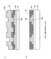
図6は、共通配線層130形成後におけるLED/駆動IC複合チップの一部を概略的に示す平面図である。共通配線層130は、LEDエピフィルム110の共通電極層116(図4に示す)と、Si基板101の集積回路102の共通電極端子107とを電気的に接続する。共通配線層130は、例えば、薄膜のメタル配線である。共通配線層130は、▲1▼金を含む単層又は積層のメタル層、例えば、金で構成された層(Au層)、チタンと白金と金の積層層(Ti/Pt/Au積層層)、金と亜鉛の積層層(Au/Zn積層層)、金・ゲルマニウム・ニッケルを含む層と金層との積層層(AuGeNi/Au積層層)、▲2▼パラジウムを含む単層又は積層のメタル層、例えば、パラジウムで構成された層(Pd層)、パラジウムと金の積層層(Pd/Au積層層)、▲3▼アルミニウムを含む単層又は積層のメタル層、例えば、アルミニウムで構成された層(Al層)、アルミニウムとニッケルの積層層(Al/Ni積層層)、▲4▼ポリシリコンで構成された層、▲5▼ITOやZnO等の導電性酸化物薄膜等とすることができる。共通配線層130は、フォトリソグラフィ技術を用いて形成することができる。
【0027】
また、共通配線層130とLEDエピフィルム110の表面及び側面との間、共通配線層130とSi基板101の表面との間、共通配線層130と集積回路102との間等のように、電気的にショートしてはならない領域には、絶縁膜(図示せず)が設けられ、正常な動作を確保できる構造になっている。LEDエピフィルム110上と集積回路102の共通電極端子107との間には、LEDエピフィルム110やIC形成領域の段差が存在する。これらの段差領域で、共通配線層116に断線が発生しないようにし良好な被覆を可能にするために、PCVD(プラズマ化学気相成長)法で形成した絶縁膜によって層間絶縁膜を形成したり、又は、ポリイミド膜等で段差を平坦化する等、段差の形態に応じて層間絶縁膜を設けることが望ましい。
【0028】
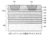
次に、LEDエピフィルム110の製造プロセスを説明する。図7から図9までは、LEDエピフィルム110の製造プロセスを概略的に示す断面図であり、図10は、図9をS10−S10線で切る面を概略的に示す断面図である。なお、図9は、図10をS9−S9線で切る面を示す断面図に相当する。
【0029】
LEDエピタキシャル層110c(剥離される前は「LEDエピタキシャル層110c」と記載し、剥離された後は「LEDエピフィルム110」と記載する。)の製造は、有機金属化学蒸着法(MOCVD法)や分子線エピタキシー法(MBE法)等によって行うことができる。LEDエピタキシャル層110cの製造に際しては、図7に示されるように、GaAs基板141上に、GaAsバッファ層142、(AlGa)InPエッチングストップ層143、及びAlAs剥離層144を順に成膜する。次に、AlAs剥離層144上に、GaAsコンタクト層111(n型GaAs層111)、AlGaAs下クラッド層112(n型AlxGa1−xAs層112)、AlGaAs活性層113(n型AlyGa1−yAs層113)、及びAlGaAs上クラッド層114(n型AlzGa1−zAs層114)を順に成膜する。LEDエピフィルム110の剥離は、化学的リフトオフ法を用いて行うことができる。ここで、エッチングストップ層143を省くこともできる。また、LEDエピタキシャル層110c及びLEDエピフィルム形成用基板140に他の半導体エピタキシャル層を追加するなど種々の変形が可能である。
【0030】
次に、図8に示されるように、固相拡散法等により亜鉛(Zn)からなるP型不純物を拡散し、Zn拡散領域115を形成する。その後、固相拡散時に用いた拡散源膜は除去し、GaAsコンタクト層のZn拡散領域表面を露出させる。
【0031】
次に、図9及び図10に示されるように、10%HF(弗化水素)液により、AlAs剥離層144を選択的に除去する。AlAs剥離層144に対するエッチング速度は、AlGaAs層112〜114、GaAs層111,141,142、及びエッチングストップ層143に対するエッチング速度に比べ格段に大きいので、AlAs剥離層144を選択的にエッチングすることができる。これにより、LEDエピフィルム110を、LEDエピフィルム製造用基板140から剥がすことが可能になる。なお、このLEDエピフィルム110を薄くするとともに、比較的短い時間でLEDエピフィルム製造用基板140から剥がすためには、例えば、LEDエピフィルム110の幅を300μm以下、例えば、50μm程度とすることが望ましい。このためには、図10に示されるように、幅W1が50μmとなるように、各エピタキシャル層111〜114をエッチングし、溝145を形成しておく。溝145の形成は、溝形成領域レジスト等によりマスクをしておき、燐酸過水によりエッチングするフォトリソグラフィ工程により行う。燐酸過水は、AlGaAs層112〜114、GaAs層111,141,142は、エッチングするが、(AlGa)InPエッチングストップ層143に対するエッチング速度が遅いので、上面から溝145をエッチング形成する際に溝が基板141まで到達するのを防止することができる。溝145を形成するにあたり溝形成予定領域上の絶縁膜をあらかじめ除去した構造とした後に、溝145を形成してもよい。溝145を形成するためのフォトリソ、エッチング工程で、溝145を形成するためのレジストマスクを使って溝形成予定領域上の絶縁膜を除去し、さらに溝形成のためのエッチングを行ってもよい。溝145を形成した後、HF液によりエッチングすることにより、AlAs剥離層144をエッチングし、LEDエピフィルム110を剥離する。なお、図10には、AlAs剥離層144が残されている状態(エッチング途中)が示されているが、LEDエピフィルム110を保持した状態で、AlAs剥離層144は完全に除去される。AlAs剥離層144をエッチング除去した後、エッチング液が残留しないように純水による水洗処理を施す。LEDエピフィルム110の剥離に際して、LEDエピフィルムを支持及び保護する支持体をLEDエピフィルム110上に設けることができる。例えば、LEDエピフィルム110の上に支持体を設けた場合、LEDエピフィルム支持体表面を、例えば、真空吸着や光硬化性粘着シート(光照射により粘着性を失う粘着シート)等により吸着し所定の位置に移動することができる。
【0032】
図11(a)から(d)までは、第1の実施形態に係るLED/駆動IC複合チップにおけるLEDエピフィルムのボンディングプロセスを概略的に示す断面図である。図11(a)に示されるように、基板140から剥離されたLEDエピフィルム110(図9及び図10に示される剥離前のLEDエピタキシャル層110c)は、第1の支持体150の光硬化性粘着シート150aによって支持され、図11(b)に示されるように、第2の支持体160上に光硬化性粘着シート160aに付着させる。次に、光照射(例えば、UV照射)によって、第1の支持体150の光硬化性粘着シート150aの粘着性を消失させ、その後、図11(d)に示されるように、第2の支持体160の位置を反転させることによって、LEDエピフィルム110を上下反転させる。この状態で、LEDエピフィルム110をSi基板101の平坦化領域103上(又はその上に形成された平坦化膜104上)に貼り付け、光照射(例えば、UV照射)によって、第2の支持体160の光硬化性粘着シート160aの粘着性を消失させ、第2の支持体160を引き離す。
【0033】
以上説明したように、第1の実施形態に係るLED/駆動IC複合チップ100によれば、Si基板101に形成された集積回路102の表面に平坦化領域103を形成し、この平坦化領域103上に平坦化膜104を設け、その上にLEDエピフィルム110を接着した構造としたので、LEDエピフィルム110に個別電極のためのワイヤボンド用電極パッドを設ける必要がない。また、第1の実施形態に係るLED/駆動IC複合チップ100によれば、共通配線層130をフォトリソグラフィ技術を用いて形成された薄膜の層としたので、LEDエピフィルム110に共通電極のためのワイヤボンド用電極パッドを設ける必要がない。このため、LEDエピフィルム110の面積を小さくでき、その結果、LED/駆動IC複合チップ100の小型化を実現できる。また、LEDエピフィルム110の面積を小さくできるので、材料コストの低減を図ることができる。
【0034】
また、第1の実施形態に係るLED/駆動IC複合チップ100によれば、LEDエピフィルム110の厚さをワイヤボンドに対する強度を考慮して厚くする必要がない。このように、LEDエピフィルム110の厚さを薄くできるので、材料コストの低減を図ることができる。
【0035】
さらに、第1の実施形態に係るLED/駆動IC複合チップ100によれば、LEDエピフィルム110のLED120側の第1の面110aをSi基板101の平坦化領域103側にし、平坦化膜104のメタル層105に重ねているので、各LED120を集積回路102に接続するための個別配線層を設ける必要がなく、構成及び製造プロセスの簡素化を実現できる。
【0036】
さらにまた、第1の実施形態に係るLED/駆動IC複合チップ100によれば、集積回路102上の平坦化領域103上にLEDエピフィルム110を備えているので、集積回路102を有するSi基板の幅を大幅に削減できる。
【0037】
また、第1の実施形態に係るLED/駆動IC複合チップ100によれば、複数の共通配線層130をLED120の配列方向に均等配列しているので、LEDエピフィルム110の共通電極層116の電位のばらつきを小さくでき、各LED120の発光強度のばらつきを小さくすることができる。
【0038】
図12は、本発明の第1の実施形態の変形例に係る半導体複合装置としてのLED/駆動IC複合チップ170を概略的に示す断面図である。図12において、図6(第1の実施形態)の構成と同一又は対応する構成には、同じ符号を付す。図12に示されたLED/駆動IC複合チップ170は、共通配線層131の形状が、図6に示される共通配線層130と相違する。図12に示されるLED/駆動IC複合チップ170においては、共通配線層131は、複数のLED120上の開口部131aを除いて、LEDエピフィルム110のほぼ全域に広がる形状をしている。共通配線層131としては、透明電極や半透明電極を用いることもできる。この場合には、LEDエピフィルム110の共通電極層116の電位のばらつきを小さくすることができ、各LED120の発光強度のばらつきを小さくすることができる。
【0039】
<第2の実施形態>
図13は、本発明の第2の実施形態に係るLED/駆動IC複合チップの一部を概略的に示す斜視図であり、図14は、LEDエピフィルムのボンディング前における第2の実施形態に係るLED/駆動IC複合チップを概略的に示す斜視図である。また、図15は、図13をS15−S15線で切る面を概略的に示す断面図である。
【0040】
図13において、図1(第1の実施形態)の構成と同一又は対応する構成には、同じ符号を付す。また、図14において、図2(第1の実施形態)の構成と同一又は対応する構成には、同じ符号を付す。また、図15において、図4(第1の実施形態)の構成と同一又は対応する構成には、同じ符号を付す。図13及び図14に示されたLED/駆動IC複合チップ200は、各メタル層105上に1個のLEDエピフィルム210を貼り付け、且つ、各LEDエピフィルム210が1個のLEDを有する点が、図1及び図2に示される第1の実施形態に係るLED/駆動IC複合チップ100と相違する。
【0041】
図15に示されるように、LEDエピフィルム210は、p型GaAs層215上に、p型AlxGa1−xAs層214、p型AlyGa1−yAs層213、n型AlzGa1−zAs層212、及びn型GaAs層211を順に形成した構造を持つ。LEDエピフィルム210の製造に際しては、第1の実施形態と同様に、LEDエピフィルム製造用基板上に、n型GaAs層211、n型AlzGa1−zAs層212、p型AlyGa1−yAs層213、p型AlxGa1−xAs層214、及びp型GaAs層215を順に成膜する。LEDエピフィルム210のボンディングに際しては、第1の実施形態と同様に、LEDエピフィルム製造用基板からLEDエピフィルム210を剥離し、LEDが形成された側の第1の面210aを平坦化領域103側にするように上下を反転させ、LEDエピフィルム210をSi基板101上のメタル層105に貼り付ける。その後、開口部230aを有する共通電極層230を形成する。共通電極層230は、第1の実施形態における共通電極層130と同様に、LEDエピフィルム210の共通電極領域上から集積回路102の共通電極端子上まで延びる薄膜の配線層である。上記各層のAl組成は、x>y且つz>y(例えば、x=z=0.4、y=0.1)とすることができる。ただし、LEDエピフィルム210の構造及び組成は上記したものに限定されない。例えば、シングルへテロ型でも、ホモ型でもよく、ダブルへテロ型においても、クラッド層の間にノンドープの活性層を設ける、又は、量子井戸層を挿入する等の種々の構造が可能である。また、p型とn型を逆にする等の変形も可能である。
【0042】
以上説明したように、第2の実施形態に係るLED/駆動IC複合チップ200によれば、LEDエピフィルム210が小さく分割されているので、LEDエピフィルム210の熱膨張係数とSi基板101の熱膨張係数とが大きく異なる場合に問題となり得る、LEDエピフィルム210の内部応力を軽減でき、LEDエピフィルム210の欠陥の発生要因の一つを排除できる。このため、第2の実施形態に係るLED/駆動IC複合チップ200の信頼性を高めることができる。
【0043】
また、第2の実施形態に係るLED/駆動IC複合チップ200によれば、LEDエピフィルム210が小さく分割されており、接着領域が小さいので、LEDエピフィルム210をメタル層105に密着させるプロセスが容易であり、密着性の不完全さに起因する欠陥発生率を低減できる。
【0044】
さらに、第2の実施形態に係るLED/駆動IC複合チップ200によれば、LEDエピフィルム210が発光領域以外の部分を持たないのでLEDエピフィルム210の幅を狭くすることができ、共通配線層の長さを短くすることができる。
【0045】
なお、第2の実施形態において、上記以外の点は、上記第1の実施形態の場合と同じである。
【0046】
<第3の実施形態>
図16は、本発明の第3の実施形態に係るLED/駆動IC複合チップの一部を概略的に示す斜視図であり、図17は、LEDエピフィルム310のボンディング前におけるLED/駆動IC複合チップを概略的に示す斜視図である。また、図18は、LED/駆動IC複合チップの一部を概略的に示す平面図である。
【0047】
図16から図18までに示されるように、第3の実施形態に係るLED/駆動IC複合チップ300は、集積回路302を有するSi基板301と、このSi基板301の表面に形成された平坦化領域303と、この平坦化領域303上に形成された平坦化膜304とを備えている。平坦化領域303は、Si基板301の表面上に絶縁膜(図示せず)を形成し、この絶縁膜が形成された面を平坦化処理(例えば、CMP処理)した領域である。第3の実施形態において、平坦化領域303は、Si基板301の集積回路302上に形成されているが、Si基板301上の集積回路302に隣接する領域に形成してもよい。また、第3の実施形態における平坦化膜304は、メタル層305である。
【0048】
また、図16から図18までに示されるように、LED/駆動IC複合チップ300は、LED320を含み、平坦化膜304上に貼り付けられた(ボンディングされた)シート状のLEDエピフィルム310を備えている。LEDエピフィルム310は、LED320が形成された側の第1の面310aの反対側の第2の面310bに共通電極層(図示せず)を有し、第2の面310bをSi基板301の平坦化領域303側にして、メタル層305に貼り付けている。なお、平坦化膜304(メタル層305)を備えずに、LEDエピフィルム310をSi基板301の平坦化領域303の表面(例えば、電極領域)上に直接貼り付けることも可能である。
【0049】
また、図16及び図18に示されるように、LED/駆動IC複合チップ300は、LEDエピフィルム310のLED320上から集積回路302の個別電極端子308上に至る領域に形成された薄膜の個別配線層330を備えている。
なお、個別配線層330の下には、適宜層間絶縁膜(図示せず)が備えられる。
【0050】
以上説明したように、第3の実施形態に係るLED/駆動IC複合チップ300によれば、LEDエピフィルム310の第2の面310bをメタル層305に接着する構造を採用しているので、より強い接着強度を得ることができる。
【0051】
なお、第3の実施形態において、上記以外の点は、上記第1又は第2の実施形態の場合と同じである。
【0052】
<第4の実施形態>
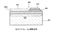
図19は、本発明の第4の実施形態に係るLED/駆動IC複合チップの一部を概略的に示す示す斜視図であり、図20は、LEDエピフィルムのボンディング前におけるLED/駆動IC複合チップを概略的に示す斜視図である。また、図21は、LED/駆動IC複合チップの一部を概略的に示す平面図であり、図22は、図21をS22−S22線で切る面を概略的に示す断面図である。
【0053】
図19から図21までに示されるように、第4の実施形態に係るLED/駆動IC複合チップ400は、集積回路402を有するSi基板401と、このSi基板401の表面に形成された平坦化領域403と、この平坦化領域403上に形成されたメタル層405とを備えている。平坦化領域403は、Si基板401の表面上に絶縁膜(図示せず)を形成し、この絶縁膜が形成された面を平坦化処理(例えば、CMP処理)した領域である。第4の実施形態においては、平坦化領域403は、Si基板401の集積回路402上及び集積回路に隣接する領域403aに形成されている。集積回路が形成された領域に隣接する領域403a上には、メタル層405が形成されており、メタル層405の表面にLEDエピフィルム410が貼り付けられ(ボンディングされ)ている。
【0054】
また、図19から図21までに示されるように、LED/駆動IC複合チップ400は、LED420を含み、メタル層405上に貼り付けられたシート状のLEDエピフィルム410を備えている。LEDエピフィルム410は、LED420が形成された側の第1の面410aの反対側の第2の面410bに共通電極層(図示せず)を有し、第2の面410bをSi基板301の平坦化領域403側にして、メタル層405に貼り付けている。ただし、第1の実施形態と同様に、メタル層を複数形成し、第1の面410aのLED420をメタル層に重ねるように形成してもよい。また、第2の実施形態と同様に、1個のLEDを有するLEDエピフィルムを複数個、メタル層上に配列してもよい。さらに、メタル層405を備えずに、LEDエピフィルム410をSi基板401の平坦化領域403aの表面(例えば、電極領域)上に直接貼り付けることも可能である。
【0055】
また、図19及び図21に示されるように、LED/駆動IC複合チップ400は、LEDエピフィルム410のLED420上から集積回路402の個別電極端子408上に至る領域に形成された薄膜の個別配線層430を備えている。
なお、個別配線層430の下(例えば、メタル層405との間)には、適宜層間絶縁膜(図示せず)が備えられる。
【0056】
以上説明したように、第4の実施形態に係るLED/駆動IC複合チップ400によれば、LEDエピフィルム410をSi基板401の集積回路402の表面(凹凸を有する表面)402aよりも高い位置に貼り付けることができる。このため、LEDエピフィルム410をメタル層405上に貼り付けるプロセスにおいて使用される装置の一部(例えば、ボンディングコレット)が集積回路502の表面(凸部)402aに当たるという不具合を回避し易い。
【0057】
なお、第4の実施形態において、上記以外の点は、上記第1から第3までの実施形態の場合と同じである。
【0058】
<第5の実施形態>
図23は、本発明の第5の実施形態に係るLED/駆動IC複合チップを概略的に示す断面図である。
【0059】
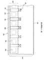
第5の実施形態に係るLED/駆動IC複合チップ500は、集積回路502を有するSi基板501と、Si基板501の集積回路502が形成された領域に隣接する領域503に形成され、集積回路502が形成された領域よりも高い位置に表面504aを持つかさあげ層504と、かさあげ層504上に形成されたメタル層505と、メタル層505の表面に貼り付けられたLEDエピフィルム510とを有する。かさあげ層504の材質及び構成は、自由に選択できるが、メタル層505と電気的に接続された配線層及びその周辺領域に形成された絶縁層を含むことができる。
【0060】
以上説明したように、第5の実施形態に係るLED/駆動IC複合チップ500によれば、LEDエピフィルム510をSi基板501の集積回路502の表面(凹凸を有する表面)502aよりも高い位置に貼り付けることができる。このため、LEDエピフィルム510をかさあげ層504上のメタル層505上に貼り付けるプロセスにおいて使用される装置の一部(例えば、ボンディングコレット)が集積回路502の表面(凸部)502aに当たるという問題を回避し易い。
【0061】
なお、第5の実施形態において、上記以外の点は、上記第1から第4までの実施形態の場合と同じである。
【0062】
<本発明が適用されたLEDプリントヘッド>
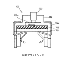
図24は、本発明に係る半導体複合装置を組み込んだLEDプリントヘッド700を概略的に示す断面図である。図24に示されるように、LEDプリントヘッド700は、ベース部材701と、ベース部材701に固定されたLEDユニット702と、柱状の光学素子を多数配列したロッドレンズアレイ703と、ロッドレンズアレイ703を保持するホルダ704と、これらの構成701〜704を固定するクランプ705とを有する。LEDユニット702には、上記実施形態の半導体複合装置であるLED/駆動ICチップが搭載されている。LEDユニット702で発生した光はロッドレンズアレイ703を通して照射される。
LEDプリントヘッド700は、電子写真プリンタや電子写真コピー装置等の露光装置として用いられる。
【0063】
<可能な変形例>
なお、上記実施形態においては、Si基板上の平坦化膜がメタル層を含む場合を説明したが、メタル層に代えてポリシリコンや、ITO、ZnO等の導電性酸化物等の金属以外の導電性薄膜層を用いてもよい。
【0064】
また、上記実施形態においては、半導体基板としてSi基板上を用いた場合を説明したが、半導体基板の材料には、アモルファスシリコン、単結晶シリコン、ポリシリコンの他、化合物半導体、有機半導体のような他の材料を用いることもできる。
【0065】
また、上記実施形態においては、半導体薄膜に備えられた半導体素子が、LEDである場合を説明したが、半導体素子は、レーザー等の他の発光素子、受光素子、ホール素子、及びピエゾ素子等のような他の素子であってもよい。
【0066】
また、上記実施形態においては、LEDエピフィルムがエピタキシャル層から構成された場合を説明したが、エピタキシャル層ではない半導体薄膜を採用してもよい。
【0067】
また、上記実施形態においては、半導体基板上の平坦化領域上に又は平坦化膜上にLEDエピフィルムを貼り付けた場合を説明したが、半導体基板上の表面の凹凸が小さい場合には、平坦化処理(例えば、CMP処理)が行われていない領域上にLEDエピフィルムを貼り付けてもよい。
ともできる。
【0068】
【発明の効果】
以上説明したように、本発明によれば、半導体基板の表面に平坦化領域を形成し、この平坦化領域上に又は平坦化膜を介在させて半導体薄膜を貼り付けた構造としたので、半導体薄膜にワイヤボンド用電極パッドを設けなくてもよく、半導体薄膜の面積を小さくでき、その結果、半導体装置の小型化を実現できる。また、半導体薄膜の面積を小さくできるので、材料コストの低減を図ることができる。
【0069】
また、半導体薄膜の半導体素子が形成された側の第1の面を平坦化領域側にした場合には、半導体薄膜と半導体基板の集積回路とを接続するための配線層を減らすことができ、構成及び製造プロセスの簡素化を実現できる。
【図面の簡単な説明】
【図1】本発明の第1の実施形態に係るLED/駆動IC複合チップの一部を概略的に示す斜視図である。
【図2】LEDエピフィルムのボンディング前における第1の実施形態に係るLED/駆動IC複合チップを概略的に示す斜視図である。
【図3】第1の実施形態に係るLED/駆動IC複合チップの一部を概略的に示す平面図である。
【図4】図3をS4−S4線で切る面を概略的に示す断面図である。
【図5】(a)及び(b)は、第1の実施形態に係るLED/駆動IC複合チップの平坦化膜の形成プロセスを概略的に示す断面図である。
【図6】共通配線層形成後における第1の実施形態に係るLED/駆動IC複合チップの一部を概略的に示す平面図である。
【図7】第1の実施形態に係るLED/駆動IC複合チップのLEDエピフィルムの製造プロセス(その1)を概略的に示す断面図である。
【図8】第1の実施形態に係るLED/駆動IC複合チップのLEDエピフィルムの製造プロセス(その2)を概略的に示す断面図である。
【図9】第1の実施形態に係るLED/駆動IC複合チップのLEDエピフィルムの製造プロセス(その3)を概略的に示す断面図である。
【図10】図9をS10−S10線で切る面を概略的に示す断面図である。
【図11】(a)から(d)までは、第1の実施形態に係るLED/駆動IC複合チップにおけるLEDエピフィルムのボンディングプロセスを概略的に示す断面図である。
【図12】第1の実施形態の変形例に係るLED/駆動IC複合チップの一部を概略的に示す平面図である。
【図13】本発明の第2の実施形態に係るLED/駆動IC複合チップの一部を概略的に示す斜視図である。
【図14】LEDエピフィルムのボンディング前における第2の実施形態に係るLED/駆動IC複合チップを概略的に示す斜視図である。
【図15】図13をS15−S15線で切る面を概略的に示す断面図である。
【図16】本発明の第3の実施形態に係るLED/駆動IC複合チップの一部を概略的に示す斜視図である。
【図17】LEDエピフィルムのボンディング前における第3の実施形態に係るLED/駆動IC複合チップを概略的に示す斜視図である。
【図18】第3の実施形態に係るLED/駆動IC複合チップの一部を概略的に示す平面図である。
【図19】本発明の第4の実施形態に係るLED/駆動IC複合チップの一部を概略的に示す示す斜視図である。
【図20】LEDエピフィルムのボンディング前における第4の実施形態に係るLED/駆動IC複合チップを概略的に示す斜視図である。
【図21】第4の実施形態に係るLED/駆動IC複合チップの一部を概略的に示す平面図である。
【図22】図21をS22−S22線で切る面を概略的に示す断面図である。
【図23】本発明の第5の実施形態に係るLED/駆動IC複合チップの概略的に示す断面図である。
【図24】本発明に係る半導体複合装置を組み込んだLEDプリントヘッドを概略的に示す断面図である。
【図25】従来のLEDプリントヘッドの一部を概略的に示す斜視図である。
【図26】図25のLEDプリントヘッドに備えられたLEDアレイチップの一部を示す平面図である。
【符号の説明】
100,170,200,300,400,500 LED/駆動IC複合チップ、
101,301,401,501 Si基板、
102,302,402,502 集積回路、
103,303,403 平坦化領域、
104,304 平坦化膜、
105,305,405,505 メタル層、
106 層間絶縁膜、
107 集積回路の共通電極端子、
110,210,310,410,510 エピタキシャルフィルム(LEDエピフィルム)、
110a,210a,310a 第1の面、
110b,210b,310b 第2の面、
110c 半導体エピタキシャル層、
111 GaAsコンタクト層(n型GaAs層)、
112 AlGaAs下クラッド層(n型AlxGa1−xAs層)、
113 AlGaAs活性層(n型AlyGa1−yAs層)、
114 AlGaAs上クラッド層(n型AlzGa1−zAs層)、
115 Zn拡散領域、
116 共通電極層、
120,320,420 LED(発光部)、
130,131,230 共通配線層、
140 LEDエピフィルム製造用基板、
141 GaAs基板、
142 GaAsバッファ層、
143 (AlGa)InPエッチングストップ層、
144 AlAs剥離層、
145 エッチング溝、
150 第1の支持体、
160 第2の支持体、
211 GaAs層、
212 p型AlxGa1−xAs層、
213 p型AlyGa1−yAs層、
214 n型AlzGa1−zAs層、
215 n型GaAs層、
230a 共通配線層の開口部、
308,408 集積回路の個別端子領域、
402a,502a 集積回路の表面、
403a,503 集積回路が形成された領域に隣接する領域、
430 集積回路の個別電極端子、
504 かさあげ層、
504a かさあげ層の表面、
700 LEDプリントヘッド、
702 LEDユニット、
703 ロッドレンズアレイ。[0001]
TECHNICAL FIELD OF THE INVENTION
The present invention relates to a semiconductor composite device such as an LED print head used in an electrophotographic printer.
[0002]
[Prior art]
FIG. 25 is a perspective view schematically showing a part of a conventional LED print head, and FIG. 26 is a plan view showing an example of an LED array chip that can be provided in the LED print head of FIG. The illustrated
[0003]
Patent Document 1 below discloses a light-emitting element having a thin film structure.
[0004]
[Patent Document 1]
JP 10-063807 A (FIGS. 3 to 6, FIG. 8, paragraph 0021)
[0005]
[Problems to be solved by the invention]
However, in the
[0006]
Further, the region functioning as the
[0007]
Further, Patent Document 1 discloses a light emitting element having a thin film structure. The light emitting element is provided with an electrode pad for a solder ball, and individual electrodes are connected to the electrode pad via the solder ball. Have been. As described above, since the light-emitting element having a thin film structure disclosed in Patent Document 1 includes the electrode pads, it is difficult to reduce the area thereof.
[0008]
SUMMARY OF THE INVENTION The present invention has been made to solve the above-described problems of the related art, and an object of the present invention is to provide a semiconductor composite device capable of reducing the size and the material cost. It is in.
[0009]
[Means for Solving the Problems]
A semiconductor composite device according to the present invention includes a semiconductor substrate having an integrated circuit, a flattened region formed on a surface of the semiconductor substrate, a semiconductor thin film having a semiconductor element, and a semiconductor thin film attached on the flattened region. It is characterized by having.
[0010]
Another semiconductor composite device according to the present invention is a semiconductor substrate having an integrated circuit, and a region formed on a region of the semiconductor substrate adjacent to a region where the integrated circuit is formed, wherein the integrated circuit is formed. It is characterized by comprising a raised layer having a surface at a higher position and a semiconductor thin film adhered on the surface of the raised layer.
[0011]
Further, still another semiconductor composite device according to the present invention includes a semiconductor substrate having an integrated circuit, and a semiconductor thin film attached to the semiconductor substrate, wherein the semiconductor thin film has the semiconductor element formed thereon. The first surface on the side is the semiconductor substrate side.
[0012]
BEST MODE FOR CARRYING OUT THE INVENTION
<First embodiment>
FIG. 1 is a perspective view schematically showing a part of an LED / drive IC composite chip which is a semiconductor composite device according to a first embodiment of the present invention, and FIG. FIG. 2 is a perspective view schematically showing a / drive IC composite chip. FIG. 3 is a plan view schematically showing a part of the LED / drive IC composite chip, and FIG. 4 -S 4 It is sectional drawing which shows the surface cut | disconnected by a line schematically.
[0013]
As shown in FIGS. 1 to 4, the LED / drive
[0014]
As shown in FIGS. 1 to 4, the LED / drive
[0015]
Further, as shown in FIGS. 1 to 4, the LED / drive
[0016]
A plurality of LEDs (light emitting portions) 120 are formed on the
[0017]
It is desirable that the LED epi-
[0018]
The
[0019]
The flattening
[0020]
FIGS. 5A and 5B are cross-sectional views schematically showing a process of forming the flattening
[0021]
As shown in FIG. 2 or FIG. 4, the LED epi-
[0022]
Next, a sectional structure of the LED / drive
[0023]
As shown in FIG. 4, the LED epi-
[0024]
The thickness of the n-
[0025]
Further, the Al composition of each of the above layers can be set so that x> y and z> y (for example, x = z = 0.4, y = 0.1). The diffusion front of the
With this configuration, the minority carriers injected through the pn junction are n-type Al y Ga 1-y Al in the As
[0026]
FIG. 6 is a plan view schematically showing a part of the LED / drive IC composite chip after the
[0027]
In addition, for example, between the
[0028]
Next, a manufacturing process of the
[0029]
The manufacture of the
[0030]
Next, as shown in FIG. 8, a P-type impurity made of zinc (Zn) is diffused by a solid phase diffusion method or the like to form a
[0031]
Next, as shown in FIGS. 9 and 10, the AlAs
[0032]
FIGS. 11A to 11D are cross-sectional views schematically showing a bonding process of an LED epi film in the LED / drive IC composite chip according to the first embodiment. As shown in FIG. 11A, the LED epi-
[0033]
As described above, according to the LED / drive
[0034]
Further, according to the LED / drive
[0035]
Further, according to the LED / drive
[0036]
Furthermore, according to the LED / drive
[0037]
Further, according to the LED / drive
[0038]
FIG. 12 is a cross-sectional view schematically showing an LED / drive
[0039]
<Second embodiment>
FIG. 13 is a perspective view schematically showing a part of the LED / drive IC composite chip according to the second embodiment of the present invention, and FIG. 14 is a perspective view showing the second embodiment before bonding the LED epi film. FIG. 4 is a perspective view schematically showing such an LED / drive IC composite chip. FIG. 15 shows FIG. Fifteen -S Fifteen It is sectional drawing which shows the surface cut | disconnected by a line schematically.
[0040]
In FIG. 13, the same or corresponding components as those in FIG. 1 (first embodiment) are denoted by the same reference numerals. In FIG. 14, the same reference numerals are given to the same or corresponding components as those in FIG. 2 (first embodiment). In FIG. 15, the same reference numerals are given to configurations that are the same as or correspond to the configurations in FIG. 4 (first embodiment). The LED / drive
[0041]
As shown in FIG. 15, the LED epi-
[0042]
As described above, according to the LED / drive
[0043]
Further, according to the LED / drive
[0044]
Further, according to the LED / driving IC
[0045]
In the second embodiment, the other points are the same as those in the first embodiment.
[0046]
<Third embodiment>
FIG. 16 is a perspective view schematically showing a part of the LED / drive IC composite chip according to the third embodiment of the present invention, and FIG. 17 is an LED / drive IC composite before bonding the LED epi-
[0047]
As shown in FIGS. 16 to 18, the LED / drive
[0048]
As shown in FIGS. 16 to 18, the LED / drive
[0049]
As shown in FIGS. 16 and 18, the LED / drive
Note that an interlayer insulating film (not shown) is provided below the
[0050]
As described above, the LED / drive
[0051]
In the third embodiment, the other points are the same as those in the first or second embodiment.
[0052]
<Fourth embodiment>
FIG. 19 is a perspective view schematically showing a part of the LED / drive IC composite chip according to the fourth embodiment of the present invention, and FIG. 20 is an LED / drive IC composite before bonding the LED epi-film. It is a perspective view which shows a chip | tip schematically. FIG. 21 is a plan view schematically showing a part of the LED / drive IC composite chip, and FIG. 22 -S 22 It is sectional drawing which shows the surface cut | disconnected by a line schematically.
[0053]
As shown in FIGS. 19 to 21, an LED / drive
[0054]
As shown in FIGS. 19 to 21, the LED / drive
[0055]
As shown in FIGS. 19 and 21, the LED / driving IC
Note that an interlayer insulating film (not shown) is appropriately provided below the individual wiring layer 430 (for example, between the individual wiring layers 430 and the metal layer 405).
[0056]
As described above, according to the LED / driving IC
[0057]
In the fourth embodiment, the other points are the same as those in the first to third embodiments.
[0058]
<Fifth embodiment>
FIG. 23 is a sectional view schematically showing an LED / drive IC composite chip according to a fifth embodiment of the present invention.
[0059]
The LED / drive
[0060]
As described above, according to the LED / drive
[0061]
In the fifth embodiment, the other points are the same as those in the first to fourth embodiments.
[0062]
<LED print head to which the present invention is applied>
FIG. 24 is a cross-sectional view schematically showing an
The
[0063]
<Possible modifications>
In the above embodiment, the case where the planarization film on the Si substrate includes a metal layer has been described. However, instead of the metal layer, a conductive material other than a metal such as polysilicon or a conductive oxide such as ITO or ZnO may be used. A conductive thin film layer may be used.
[0064]
Further, in the above embodiment, the case where a Si substrate is used as the semiconductor substrate has been described, but the material of the semiconductor substrate may be amorphous silicon, single crystal silicon, polysilicon, compound semiconductor, organic semiconductor, or the like. Other materials can be used.
[0065]
Further, in the above-described embodiment, the case where the semiconductor element provided in the semiconductor thin film is an LED has been described. Such other elements may be used.
[0066]
Further, in the above embodiment, the case where the LED epi-film is constituted by the epitaxial layer has been described, but a semiconductor thin film other than the epitaxial layer may be employed.
[0067]
Further, in the above embodiment, the case where the LED epi-film is stuck on the flattened region on the semiconductor substrate or on the flattened film has been described. The LED epi film may be pasted on a region where the chemical conversion treatment (for example, the CMP treatment) is not performed.
Can also be.
[0068]
【The invention's effect】
As described above, according to the present invention, a flattened region is formed on the surface of a semiconductor substrate, and a semiconductor thin film is attached on the flattened region or with a flattening film interposed therebetween. It is not necessary to provide an electrode pad for wire bonding on the thin film, the area of the semiconductor thin film can be reduced, and as a result, the semiconductor device can be downsized. Further, since the area of the semiconductor thin film can be reduced, material cost can be reduced.
[0069]
Further, when the first surface of the semiconductor thin film on which the semiconductor element is formed is located on the flattening region side, the number of wiring layers for connecting the semiconductor thin film and the integrated circuit of the semiconductor substrate can be reduced, The configuration and the manufacturing process can be simplified.
[Brief description of the drawings]
FIG. 1 is a perspective view schematically showing a part of an LED / drive IC composite chip according to a first embodiment of the present invention.
FIG. 2 is a perspective view schematically showing the LED / drive IC composite chip according to the first embodiment before bonding of the LED epifilm.
FIG. 3 is a plan view schematically showing a part of the LED / drive IC composite chip according to the first embodiment.
FIG. 4 shows S in FIG. 4 -S 4 It is sectional drawing which shows the surface cut | disconnected by a line schematically.
FIGS. 5A and 5B are cross-sectional views schematically showing a process of forming a flattening film of the LED / drive IC composite chip according to the first embodiment.
FIG. 6 is a plan view schematically showing a part of the LED / drive IC composite chip according to the first embodiment after a common wiring layer is formed.
FIG. 7 is a cross-sectional view schematically showing a manufacturing process (part 1) of the LED epi-film of the LED / drive IC composite chip according to the first embodiment.
FIG. 8 is a sectional view schematically showing a manufacturing process (part 2) of the LED epi-film of the LED / drive IC composite chip according to the first embodiment.
FIG. 9 is a sectional view schematically showing a manufacturing process (part 3) of the LED epi-film of the LED / drive IC composite chip according to the first embodiment.
FIG. 10 shows S in FIG. 10 -S 10 It is sectional drawing which shows the surface cut | disconnected by a line schematically.
FIGS. 11A to 11D are cross-sectional views schematically showing a bonding process of an LED epi film in the LED / drive IC composite chip according to the first embodiment.
FIG. 12 is a plan view schematically showing a part of an LED / drive IC composite chip according to a modification of the first embodiment.
FIG. 13 is a perspective view schematically showing a part of an LED / drive IC composite chip according to a second embodiment of the present invention.
FIG. 14 is a perspective view schematically showing an LED / drive IC composite chip according to a second embodiment before bonding of an LED epifilm.
FIG. 15 shows S in FIG. Fifteen -S Fifteen It is sectional drawing which shows the surface cut | disconnected by a line schematically.
FIG. 16 is a perspective view schematically showing a part of an LED / drive IC composite chip according to a third embodiment of the present invention.
FIG. 17 is a perspective view schematically showing an LED / drive IC composite chip according to a third embodiment before bonding of an LED epifilm.
FIG. 18 is a plan view schematically showing a part of the LED / drive IC composite chip according to the third embodiment.
FIG. 19 is a perspective view schematically showing a part of a combined LED / drive IC chip according to a fourth embodiment of the present invention.
FIG. 20 is a perspective view schematically showing an LED / drive IC composite chip according to a fourth embodiment before bonding of an LED epifilm.
FIG. 21 is a plan view schematically showing a part of an LED / drive IC composite chip according to a fourth embodiment.
FIG. 22 shows S in FIG. 22 -S 22 It is sectional drawing which shows the surface cut | disconnected by a line schematically.
FIG. 23 is a cross-sectional view schematically showing an LED / drive IC composite chip according to a fifth embodiment of the present invention.
FIG. 24 is a cross-sectional view schematically showing an LED print head incorporating the semiconductor composite device according to the present invention.
FIG. 25 is a perspective view schematically showing a part of a conventional LED print head.
FIG. 26 is a plan view showing a part of an LED array chip provided in the LED print head of FIG. 25;
[Explanation of symbols]
100, 170, 200, 300, 400, 500 LED / drive IC composite chip,
101, 301, 401, 501 Si substrate,
102, 302, 402, 502 integrated circuits;
103, 303, 403 flattened area,
104, 304 planarization film,
105, 305, 405, 505 metal layer,
106 interlayer insulating film,
107 integrated circuit common electrode terminals,
110, 210, 310, 410, 510 epitaxial film (LED epi film),
110a, 210a, 310a first surface,
110b, 210b, 310b second surface,
110c semiconductor epitaxial layer,
111 GaAs contact layer (n-type GaAs layer),
112 AlGaAs lower cladding layer (n-type Al x Ga 1-x As layer),
113 AlGaAs active layer (n-type Al y Ga 1-y As layer),
114 AlGaAs upper cladding layer (n-type Al z Ga 1-z As layer),
115 Zn diffusion region,
116 common electrode layer,
120, 320, 420 LED (light emitting unit),
130, 131, 230 common wiring layer,
140 LED epi-film production substrate,
141 GaAs substrate,
142 GaAs buffer layer,
143 (AlGa) InP etching stop layer,
144 AlAs release layer,
145 etching grooves,
150 first support,
160 second support,
211 GaAs layer,
212 p-type Al x Ga 1-x As layer,
213 p-type Al y Ga 1-y As layer,
214 n-type Al z Ga 1-z As layer,
215 n-type GaAs layer,
230a opening of common wiring layer,
308,408 individual terminal areas of the integrated circuit;
402a, 502a surface of the integrated circuit;
403a, 503 a region adjacent to the region where the integrated circuit is formed;
430 individual electrode terminals of the integrated circuit,
504 raised layer,
504a Surface of the raising layer,
700 LED print head,
702 LED unit,
703 rod lens array.
Claims (19)
前記半導体基板の表面に形成された平坦化領域と、
半導体素子を有し、前記平坦化領域上に貼り付けられた半導体薄膜と
を備えたことを特徴とする半導体複合装置。A semiconductor substrate having an integrated circuit;
A flattened region formed on the surface of the semiconductor substrate,
A semiconductor composite device comprising: a semiconductor element; and a semiconductor thin film attached to the flattened region.
前記平坦化膜の前記半導体薄膜側の面に平坦化処理が施されている
ことを特徴とする請求項1から4までのいずれかに記載の半導体複合装置。A flattening film is interposed between the flattening region and the semiconductor thin film,
5. The semiconductor composite device according to claim 1, wherein a flattening process is performed on a surface of the flattening film on the side of the semiconductor thin film.
前記集積回路が、共通電極端子を有し、
前記半導体薄膜の前記共通電極層上から前記集積回路の前記共通電極端子上に至る領域に形成された薄膜の共通配線層を備えた
ことを特徴とする請求項7に記載の半導体複合装置。The semiconductor thin film has a common electrode layer on a second surface opposite to the first surface;
The integrated circuit has a common electrode terminal,
8. The semiconductor composite device according to claim 7, further comprising: a thin film common wiring layer formed in a region extending from the common electrode layer of the semiconductor thin film to the common electrode terminal of the integrated circuit.
前記半導体薄膜の前記半導体素子上から前記個別電極端子上に至る領域に形成された薄膜の個別配線層を備えた
ことを特徴とする請求項9に記載の半導体複合装置。The integrated circuit has an individual electrode terminal,
The semiconductor composite device according to claim 9, further comprising a thin film individual wiring layer formed in a region of the semiconductor thin film from the semiconductor element to the individual electrode terminal.
前記半導体基板の前記集積回路が形成された領域に隣接する領域上に形成され、前記集積回路が形成された領域よりも高い位置に表面を持つかさあげ層と、
前記かさあげ層の表面上に貼り付けられた半導体薄膜と
を備えたことを特徴とする半導体複合装置。A semiconductor substrate having an integrated circuit;
A raised layer formed on a region of the semiconductor substrate adjacent to the region where the integrated circuit is formed, and having a surface at a position higher than the region where the integrated circuit is formed;
A semiconductor composite device comprising: a semiconductor thin film attached to a surface of the raising layer.
前記半導体基板上に貼り付けられた半導体薄膜とを有し、
前記半導体薄膜が、前記半導体素子が形成された側の第1の面を前記半導体基板側にしたことを特徴とする半導体複合装置。A semiconductor substrate having an integrated circuit;
Having a semiconductor thin film attached on the semiconductor substrate,
A semiconductor composite device, wherein the semiconductor thin film has a first surface on a side where the semiconductor element is formed on the semiconductor substrate side.
前記集積回路が、共通電極端子を有し、
前記半導体薄膜の前記共通電極層上から前記集積回路の前記共通電極端子上に至る領域に形成された薄膜の共通配線層を備えた
ことを特徴とする請求項12から14までのいずれかに記載の半導体複合装置。The semiconductor thin film has a common electrode layer on a second surface opposite to the first surface;
The integrated circuit has a common electrode terminal,
15. The semiconductor device according to claim 12, further comprising a thin film common wiring layer formed in a region extending from above the common electrode layer of the semiconductor thin film to above the common electrode terminal of the integrated circuit. Semiconductor composite equipment.
前記集積回路が、前記半導体素子を駆動させる駆動ICを含む
ことを特徴とする請求項1から16までのいずれかに記載の半導体複合装置。The semiconductor element is a light-emitting element, a light-receiving element, a Hall element, and any one of piezo elements,
17. The semiconductor composite device according to claim 1, wherein the integrated circuit includes a driving IC for driving the semiconductor element.
Priority Applications (4)
| Application Number | Priority Date | Filing Date | Title |
|---|---|---|---|
| JP2002371724A JP4179866B2 (en) | 2002-12-24 | 2002-12-24 | Semiconductor composite device and LED head |
| EP03029114A EP1434271A3 (en) | 2002-12-24 | 2003-12-17 | Integrated semiconductor device comprising semiconductor thin films and optical print head |
| US10/743,104 US20040135157A1 (en) | 2002-12-24 | 2003-12-23 | Combined semiconductor apparatus with semiconductor thin film |
| US12/654,486 US8664668B2 (en) | 2002-12-24 | 2009-12-22 | Combined semiconductor apparatus with semiconductor thin film |
Applications Claiming Priority (1)
| Application Number | Priority Date | Filing Date | Title |
|---|---|---|---|
| JP2002371724A JP4179866B2 (en) | 2002-12-24 | 2002-12-24 | Semiconductor composite device and LED head |
Publications (3)
| Publication Number | Publication Date |
|---|---|
| JP2004207323A true JP2004207323A (en) | 2004-07-22 |
| JP2004207323A5 JP2004207323A5 (en) | 2005-07-28 |
| JP4179866B2 JP4179866B2 (en) | 2008-11-12 |
Family
ID=32463500
Family Applications (1)
| Application Number | Title | Priority Date | Filing Date |
|---|---|---|---|
| JP2002371724A Expired - Fee Related JP4179866B2 (en) | 2002-12-24 | 2002-12-24 | Semiconductor composite device and LED head |
Country Status (3)
| Country | Link |
|---|---|
| US (2) | US20040135157A1 (en) |
| EP (1) | EP1434271A3 (en) |
| JP (1) | JP4179866B2 (en) |
Cited By (8)
| Publication number | Priority date | Publication date | Assignee | Title |
|---|---|---|---|---|
| JP2006245210A (en) * | 2005-03-02 | 2006-09-14 | Oki Data Corp | Semiconductor composite apparatus, led device, led head and image forming apparatus |
| JP2006319099A (en) * | 2005-05-12 | 2006-11-24 | Oki Data Corp | Semiconductor device, print head, and image forming apparatus |
| JP2007260952A (en) * | 2006-03-27 | 2007-10-11 | Oki Data Corp | Semiconductor compound device, led head, and image forming apparatus |
| JP2009004502A (en) * | 2007-06-20 | 2009-01-08 | Oki Data Corp | Semiconductor device and led print head |
| JP2011233927A (en) * | 2011-08-02 | 2011-11-17 | Oki Data Corp | Semiconductor device, led device, led head and image forming device |
| JP2015126189A (en) * | 2013-12-27 | 2015-07-06 | 株式会社沖データ | Semiconductor device, method of manufacturing semiconductor device, optical print head and image formation device |
| EP2927958A1 (en) | 2014-03-31 | 2015-10-07 | Oki Data Corporation | Light emitting element array, semiconductor device, manufacturing method thereof, printing head and image forming apparatus |
| US9214342B2 (en) | 2009-09-17 | 2015-12-15 | Sumitomo Chemical Company, Limited | Method for producing compound semiconductor crystal, method for producing electronic device, and semiconductor wafer |
Families Citing this family (11)
| Publication number | Priority date | Publication date | Assignee | Title |
|---|---|---|---|---|
| JP2006082260A (en) * | 2004-09-14 | 2006-03-30 | Oki Data Corp | Semiconductor composite device, its manufacturing method, led head using the same and image forming apparatus using the led head |
| DE102004050371A1 (en) * | 2004-09-30 | 2006-04-13 | Osram Opto Semiconductors Gmbh | Optoelectronic component with a wireless contact |
| JP4420932B2 (en) * | 2007-03-09 | 2010-02-24 | 株式会社沖データ | Flexible display body and article with flexible display body |
| CA2739327A1 (en) * | 2008-10-10 | 2010-04-15 | Alta Devices, Inc. | Mesa etch method and composition for epitaxial lift off |
| CN103155189B (en) * | 2010-10-12 | 2017-02-22 | 皇家飞利浦电子股份有限公司 | Highly reflective coating on LED submount |
| EP2500623A1 (en) | 2011-03-18 | 2012-09-19 | Koninklijke Philips Electronics N.V. | Method for providing a reflective coating to a substrate for a light-emitting device |
| KR20130066271A (en) * | 2011-12-12 | 2013-06-20 | 한국전자통신연구원 | Method of fabricating organic light emitting diode |
| DE102012101409A1 (en) | 2011-12-23 | 2013-06-27 | Osram Opto Semiconductors Gmbh | Method for producing a plurality of optoelectronic semiconductor chips and optoelectronic semiconductor chip |
| US9576595B1 (en) | 2014-11-19 | 2017-02-21 | Seagate Technology Llc | Transfer printing an epitaxial layer to a read/write head to form an integral laser |
| DE102015115812A1 (en) * | 2015-09-18 | 2017-03-23 | Osram Opto Semiconductors Gmbh | Component and method for producing a device |
| CN109300932B (en) * | 2018-11-12 | 2024-01-23 | 严光能 | LED display and manufacturing method thereof |
Family Cites Families (30)
| Publication number | Priority date | Publication date | Assignee | Title |
|---|---|---|---|---|
| US4342102A (en) * | 1980-06-18 | 1982-07-27 | Signetics Corporation | Semiconductor memory array |
| JPS61102767A (en) | 1984-10-26 | 1986-05-21 | Agency Of Ind Science & Technol | Semiconductor memory device |
| JPS62123787A (en) | 1985-11-22 | 1987-06-05 | Nec Corp | Manufacture of semiconductor device |
| JPH0694216B2 (en) * | 1987-04-06 | 1994-11-24 | 沖電気工業株式会社 | Optical print head |
| EP0308749A3 (en) * | 1987-09-25 | 1990-07-11 | Siemens Aktiengesellschaft | Electrooptical unit |
| JP3197916B2 (en) | 1990-11-15 | 2001-08-13 | 株式会社リコー | Optical printer light source |
| GB9223306D0 (en) * | 1992-11-06 | 1992-12-23 | Bt & D Technologies Ltd | Optoelectronic devices |
| KR0124393B1 (en) * | 1994-03-18 | 1997-12-11 | 김주용 | Capacitor manufacturing method |
| JPH0945930A (en) | 1995-07-28 | 1997-02-14 | Sony Corp | Thin film transistor and its manufacture |
| US5621225A (en) * | 1996-01-18 | 1997-04-15 | Motorola | Light emitting diode display package |
| JPH1063807A (en) | 1996-08-23 | 1998-03-06 | Hitachi Ltd | Card type information controller |
| JP3859821B2 (en) * | 1997-07-04 | 2006-12-20 | 株式会社半導体エネルギー研究所 | Semiconductor device |
| JPH1197705A (en) * | 1997-09-23 | 1999-04-09 | Semiconductor Energy Lab Co Ltd | Semiconductor integrated circuit |
| JP3510479B2 (en) * | 1998-04-27 | 2004-03-29 | シャープ株式会社 | Manufacturing method of optical input / output element array device |
| JP3784177B2 (en) * | 1998-09-29 | 2006-06-07 | 株式会社沖データ | Driver IC |
| JP3100584B2 (en) | 1999-02-15 | 2000-10-16 | 日本電信電話株式会社 | Optoelectronic integrated circuit and method of manufacturing the same |
| US7288420B1 (en) * | 1999-06-04 | 2007-10-30 | Semiconductor Energy Laboratory Co., Ltd. | Method for manufacturing an electro-optical device |
| JP2001024027A (en) * | 1999-07-09 | 2001-01-26 | Oki Electric Ind Co Ltd | Semiconductor element, manufacture thereof, semiconductor device and manufacture |
| US6242324B1 (en) * | 1999-08-10 | 2001-06-05 | The United States Of America As Represented By The Secretary Of The Navy | Method for fabricating singe crystal materials over CMOS devices |
| US6410459B2 (en) * | 1999-09-02 | 2002-06-25 | Micron Technology, Inc. | Wafer planarization using a uniform layer of material and method and apparatus for forming uniform layer of material used in semiconductor processing |
| JP2001167874A (en) | 1999-09-29 | 2001-06-22 | Futaba Corp | Organic electroluminescent element and method of manufacturing the same |
| TW525305B (en) * | 2000-02-22 | 2003-03-21 | Semiconductor Energy Lab | Self-light-emitting device and method of manufacturing the same |
| US6351327B1 (en) * | 2000-05-30 | 2002-02-26 | Agilent Technologies, Inc. | Liquid crystal pixel current sensing for silicon micro displays |
| US6739931B2 (en) * | 2000-09-18 | 2004-05-25 | Semiconductor Energy Laboratory Co., Ltd. | Display device and method of fabricating the display device |
| JP2002141492A (en) | 2000-10-31 | 2002-05-17 | Canon Inc | Light-emitting diode display panel and manufacturing method thereof |
| WO2002049082A2 (en) * | 2000-12-11 | 2002-06-20 | Rodel Holdings, Inc. | Process of shaping a semiconductor substrate and/or a lithographic mask |
| US20020155795A1 (en) * | 2001-04-24 | 2002-10-24 | Mark Ferra | Optical endpoint detection for buff module on CMP tool |
| US6841813B2 (en) * | 2001-08-13 | 2005-01-11 | Matrix Semiconductor, Inc. | TFT mask ROM and method for making same |
| US6717222B2 (en) * | 2001-10-07 | 2004-04-06 | Guobiao Zhang | Three-dimensional memory |
| US7488986B2 (en) * | 2001-10-26 | 2009-02-10 | Semiconductor Energy Laboratory Co., Ltd. | Light emitting device |
-
2002
- 2002-12-24 JP JP2002371724A patent/JP4179866B2/en not_active Expired - Fee Related
-
2003
- 2003-12-17 EP EP03029114A patent/EP1434271A3/en not_active Withdrawn
- 2003-12-23 US US10/743,104 patent/US20040135157A1/en not_active Abandoned
-
2009
- 2009-12-22 US US12/654,486 patent/US8664668B2/en active Active
Cited By (12)
| Publication number | Priority date | Publication date | Assignee | Title |
|---|---|---|---|---|
| JP2006245210A (en) * | 2005-03-02 | 2006-09-14 | Oki Data Corp | Semiconductor composite apparatus, led device, led head and image forming apparatus |
| US8174028B2 (en) | 2005-03-02 | 2012-05-08 | Oki Data Corporation | Semiconductor composite apparatus, LED, LED printhead, and image forming apparatus |
| JP2006319099A (en) * | 2005-05-12 | 2006-11-24 | Oki Data Corp | Semiconductor device, print head, and image forming apparatus |
| JP4636501B2 (en) * | 2005-05-12 | 2011-02-23 | 株式会社沖データ | Semiconductor device, print head, and image forming apparatus |
| US8035115B2 (en) | 2005-05-12 | 2011-10-11 | Oki Data Corporation | Semiconductor apparatus, print head, and image forming apparatus |
| JP2007260952A (en) * | 2006-03-27 | 2007-10-11 | Oki Data Corp | Semiconductor compound device, led head, and image forming apparatus |
| JP2009004502A (en) * | 2007-06-20 | 2009-01-08 | Oki Data Corp | Semiconductor device and led print head |
| US9214342B2 (en) | 2009-09-17 | 2015-12-15 | Sumitomo Chemical Company, Limited | Method for producing compound semiconductor crystal, method for producing electronic device, and semiconductor wafer |
| JP2011233927A (en) * | 2011-08-02 | 2011-11-17 | Oki Data Corp | Semiconductor device, led device, led head and image forming device |
| JP2015126189A (en) * | 2013-12-27 | 2015-07-06 | 株式会社沖データ | Semiconductor device, method of manufacturing semiconductor device, optical print head and image formation device |
| EP2927958A1 (en) | 2014-03-31 | 2015-10-07 | Oki Data Corporation | Light emitting element array, semiconductor device, manufacturing method thereof, printing head and image forming apparatus |
| US9614125B2 (en) | 2014-03-31 | 2017-04-04 | Oki Data Corporation | Composite element chip, a semiconductor device and manufacturing method thereof, a printing head, and an image forming apparatus |
Also Published As
| Publication number | Publication date |
|---|---|
| JP4179866B2 (en) | 2008-11-12 |
| US8664668B2 (en) | 2014-03-04 |
| US20040135157A1 (en) | 2004-07-15 |
| US20100096748A1 (en) | 2010-04-22 |
| EP1434271A2 (en) | 2004-06-30 |
| EP1434271A3 (en) | 2011-01-12 |
Similar Documents
| Publication | Publication Date | Title |
|---|---|---|
| JP3813123B2 (en) | Semiconductor device and LED head | |
| JP4097510B2 (en) | Manufacturing method of semiconductor device | |
| JP4179866B2 (en) | Semiconductor composite device and LED head | |
| JP5599916B2 (en) | Semiconductor device manufacturing method, semiconductor device, optical print head using the same, and image forming apparatus | |
| US6838704B2 (en) | Light emitting diode and method of making the same | |
| USRE43411E1 (en) | Series connection of two light emitting diodes through semiconductor manufacture process | |
| JP5415191B2 (en) | Semiconductor composite device, optical print head, and image forming apparatus | |
| JP2008091862A (en) | Nitride semiconductor light emitting device, and manufacturing method of nitride semiconductor light emitting device | |
| WO2008093880A1 (en) | Semiconductor device and method for manufacturing the same | |
| CN111933765B (en) | Miniature light-emitting diode and manufacturing method thereof, and miniature LED display module and manufacturing method thereof | |
| JP2004207325A (en) | Semiconductor device | |
| US8981398B2 (en) | Semiconductor light emitting device and method for manufacturing the same | |
| JP2004179641A (en) | Semiconductor device, optical print head and image forming apparatus | |
| JP4393306B2 (en) | Semiconductor light emitting element, method for manufacturing the same, and semiconductor device | |
| KR100890468B1 (en) | Light emitting diode device using conductive interconnection part | |
| JP4277583B2 (en) | Semiconductor light emitting device | |
| KR100752348B1 (en) | Method of producing light emitting diode having vertical structure | |
| JP2941743B2 (en) | Compound semiconductor light emitting device and method of manufacturing the same | |
| JP4573867B2 (en) | Semiconductor device | |
| JP2005079369A (en) | Method for manufacturing semiconductor composite device | |
| TWI423468B (en) | Light emitting device and method for manufacturing the same | |
| JP2009290232A (en) | Method for manufacturing semiconductor composite device | |
| JP4098561B2 (en) | Electrode structure and manufacturing method thereof | |
| KR101147715B1 (en) | Semiconductor light emitting device | |
| KR20110037356A (en) | Iii-nitride semiconductor light emitting device |
Legal Events
| Date | Code | Title | Description |
|---|---|---|---|
| A521 | Request for written amendment filed |
Free format text: JAPANESE INTERMEDIATE CODE: A523 Effective date: 20041216 |
|
| A621 | Written request for application examination |
Free format text: JAPANESE INTERMEDIATE CODE: A621 Effective date: 20041216 |
|
| A977 | Report on retrieval |
Free format text: JAPANESE INTERMEDIATE CODE: A971007 Effective date: 20071102 |
|
| A131 | Notification of reasons for refusal |
Free format text: JAPANESE INTERMEDIATE CODE: A131 Effective date: 20071127 |
|
| A521 | Request for written amendment filed |
Free format text: JAPANESE INTERMEDIATE CODE: A523 Effective date: 20080128 |
|
| A131 | Notification of reasons for refusal |
Free format text: JAPANESE INTERMEDIATE CODE: A131 Effective date: 20080401 |
|
| A521 | Request for written amendment filed |
Free format text: JAPANESE INTERMEDIATE CODE: A523 Effective date: 20080530 |
|
| TRDD | Decision of grant or rejection written | ||
| A01 | Written decision to grant a patent or to grant a registration (utility model) |
Free format text: JAPANESE INTERMEDIATE CODE: A01 Effective date: 20080826 |
|
| A01 | Written decision to grant a patent or to grant a registration (utility model) |
Free format text: JAPANESE INTERMEDIATE CODE: A01 |
|
| A61 | First payment of annual fees (during grant procedure) |
Free format text: JAPANESE INTERMEDIATE CODE: A61 Effective date: 20080826 |
|
| R150 | Certificate of patent or registration of utility model |
Free format text: JAPANESE INTERMEDIATE CODE: R150 Ref document number: 4179866 Country of ref document: JP Free format text: JAPANESE INTERMEDIATE CODE: R150 |
|
| FPAY | Renewal fee payment (event date is renewal date of database) |
Free format text: PAYMENT UNTIL: 20110905 Year of fee payment: 3 |
|
| FPAY | Renewal fee payment (event date is renewal date of database) |
Free format text: PAYMENT UNTIL: 20110905 Year of fee payment: 3 |
|
| FPAY | Renewal fee payment (event date is renewal date of database) |
Free format text: PAYMENT UNTIL: 20120905 Year of fee payment: 4 |
|
| FPAY | Renewal fee payment (event date is renewal date of database) |
Free format text: PAYMENT UNTIL: 20120905 Year of fee payment: 4 |
|
| FPAY | Renewal fee payment (event date is renewal date of database) |
Free format text: PAYMENT UNTIL: 20130905 Year of fee payment: 5 |
|
| S111 | Request for change of ownership or part of ownership |
Free format text: JAPANESE INTERMEDIATE CODE: R313115 |
|
| R350 | Written notification of registration of transfer |
Free format text: JAPANESE INTERMEDIATE CODE: R350 |
|
| LAPS | Cancellation because of no payment of annual fees |