JP2004200533A - Heat radiation structure of device - Google Patents
Heat radiation structure of device Download PDFInfo
- Publication number
- JP2004200533A JP2004200533A JP2002369217A JP2002369217A JP2004200533A JP 2004200533 A JP2004200533 A JP 2004200533A JP 2002369217 A JP2002369217 A JP 2002369217A JP 2002369217 A JP2002369217 A JP 2002369217A JP 2004200533 A JP2004200533 A JP 2004200533A
- Authority
- JP
- Japan
- Prior art keywords
- heat
- heat sink
- heat dissipation
- dissipation structure
- circuit board
- Prior art date
- Legal status (The legal status is an assumption and is not a legal conclusion. Google has not performed a legal analysis and makes no representation as to the accuracy of the status listed.)
- Abandoned
Links
Images


Abstract
Description
【0001】
【発明の属する技術分野】
本発明は、電子部品の放熱構造、特に、デバイスの表面に直接ヒートシンクを取り付けて放熱するができない場合にデバイスが実装されているプリント基板から放熱させるデバイスの放熱構造に関する。
【0002】
【従来の技術】
プリント基板に実装されるデバイスからの放熱は、主に以下の4つの方法が用いられている。
(1)デバイスの表面から直接熱を大気へ逃がす方法。
(2)デバイスの表面から熱の良導体である金属等へ熱伝導させ、熱を大気へ逃がす方法(例えば、特許文献1参照。)。
(3)デバイスが実装されたプリント基板へ熱伝導させ、プリント基板から直接熱を大気に逃がす方法。
(4)デバイス表面から輻射させて大気へ熱を逃がす方法。
【0003】
しかし、上記の方法のそれぞれに対し、以下の問題がある。
上記(1)については、狭い装置筐体内の空間で、大気の流動性が悪い場合、放熱効果は期待できないという問題を有する。
また、上記(2)については、ヒートシンク等をデバイスの表面に貼り付ければ効果的に放熱を行うことができるが、デバイス表面が発光面等の場合、金属等により直接熱を逃がすためには、特殊なハウジングおよび金属ケースが必要であるという問題を有する(例えば、特許文献2参照。)。
また、上記(3)については、一般的にプリント基板の熱伝導率は低く、特に薄板、低層構成の場合は、熱の良導体としては期待できないという問題を有する。
さらに、上記(4)については、デバイス表面の輻射率に大きく影響され、光沢のある表面からは、輻射による熱移動は少ないという問題を有する。
【0004】
そこで、前記した問題に対処するため、筐体空間を大きくする、ファン等の強制空冷を用いる、または基板下に電子冷却器を取り付けて放熱させる方法が一般的に用いられている(例えば、特許文献3および特許文献4参照。)。
【0005】
【特許文献1】
特開平6−196598号公報
【特許文献2】
特開平5−3330号公報
【特許文献3】
特開平5−95062号公報
【特許文献4】
特開平7−287130号公報
【0006】
【発明が解決しようとする課題】
しかし、装置筐体の空間を大きくすると、筐体自体が大型、高重量になり、コストが高くなるという問題があった。また、ファン、電子冷却器等の強制冷却装置を用いた場合も、同様に、装置筐体の空間を大きくする必要があり、大型、高重量および高コストという問題があった。
【0007】
また、デバイスの表面が発光面等の場合、該デバイスの放熱を行うためには、デバイスのほぼ全体を取り囲む特殊なハウジングおよび金属ケースを必要とするという問題があった。
【0008】
そこで、本発明の目的は、かかる問題を解決するために、デバイスの表面を大気に接した状態で、該デバイスの放熱を小型、低重量および安価に行う放熱構造を提供することである。
【0009】
【課題を解決するための手段】
請求項1に記載のデバイスの放熱構造は、デバイスの裏面がプリント基板の表面に対向し、前記デバイスの表面が大気に接して前記プリント基板に実装されたデバイスの放熱構造において、前記デバイスを取り囲むように大気と連通する孔が設けられた凸部を有する上部放熱板と、断面略L字形状または略コ字形状の下部放熱板とを設け、前記凸部と前記下部放熱板とで前記プリント基板を密着するように挟み込み、前記上部放熱板と前記下部放熱板を連結したものである。この構成により、表面に直接放熱構造を付することができないデバイス、例えば面発光素子であっても、軽量、小型、安価で、しかも効率的にデバイスの放熱をすることができる。
【0010】
請求項2に記載のデバイスの放熱構造は、請求項1に記載のデバイスの放熱構造において、前記上部放熱板と前記プリント基板の間、および/または前記下部放熱板と前記プリント基板の間に、放熱シートを設けたものである。この構成により、デバイスの熱を、プリント基板を介して上部放熱板および/または下部放熱板に効率的に伝えることができ、表面に直接放熱構造を付することができないデバイス、例えば面発光素子であっても、軽量、小型、安価で、しかも効率的にデバイスの放熱をすることができる。
【0011】
請求項3に記載のデバイスの放熱構造は、請求項1に記載のデバイスの放熱構造において、前記上部放熱板が装置筐体の上面の一部または全部となり、前記下部放熱板が前記装置筐体の下面および側面の一部または全部となるものである。この構成により、上部放熱板および下部放熱板がそのまま装置の筐体となることから、装置筐体のコストの低減、すなわち、デバイスを搭載した装置のコストを低減することができる。
【0012】
請求項4に記載のデバイスの放熱構造は、請求項1記載のデバイスの放熱構造において、前記上部放熱板が装置筐体の上面および側面の一部または全部となり、前記下部放熱板が前記装置筐体の下面の一部または全部となるものである。この構成により、上部放熱板および下部放熱板がそのまま装置の筐体となることから、装置筐体のコストの低減、すなわち、デバイスを搭載した装置のコストを低減することができる。
【0013】
請求項5に記載のデバイスの放熱構造は、請求項1に記載のデバイスの放熱構造において、前記上部放熱板および前記下部放熱板の材質は、銅または黒アルマイト処理されたアルミニウムであるものである。この構成により、デバイスから伝わってきた熱を効率的に大気に逃がすことができる。また、金属等の基台の上に本放熱構造をもつ装置が載置された場合は、下部放熱板が銅または黒アルマイト処理されたアルミニウムからなることから、デバイスから伝わった熱を下部放熱板から前記基台に逃がすことができる。
【0014】
請求項6に記載のデバイスの放熱構造は、請求項1に記載のデバイスの放熱構造において、前記プリント基板が前記凸部と密着する部分および/または前記プリント基板が前記下部放熱板と密着する部分において、前記プリント基板の表面および/または裏面に銅箔ベタパターンが設けられているものである。この構成により、デバイスからプリント基板に伝わってきた熱を、上部放熱板および/または下部放熱板に伝え易くできる。
【0015】
請求項7に記載のデバイスの放熱構造は、請求項1に記載のデバイスの放熱構造において、前記上部放熱板および/または前記下部放熱板にヒートシンクが取り付けられているものである。この構成により、上部放熱板および/または下部放熱板の表面積が大きくなるため、上部放熱板および/または下部放熱板に溜まった熱を大気に放出し易くなる。
【0016】
請求項8に記載のデバイスの放熱構造は、請求項1に記載のデバイスの放熱構造において、前記上部放熱板および/または前記下部放熱板に複数の凹部を設け、ヒートシンクの機能を持たせたものである。この構成により、上部放熱板および/または下部放熱板の表面積が大きくなるため、上部放熱板および/または下部放熱板に溜まった熱を大気に放出し易くなる。
【0017】
【発明の実施の形態】
以下に本発明の実施の形態につき、図面を用いて詳細に説明する。
【0018】
(第1実施形態)
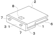
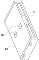
図1は、第1実施形態の放熱構造を示す斜視図であり、図2はその分解図である。図1および図2に示すように、凸部1を有する上部放熱板2と略L字形状の下部放熱板3の間に、デバイス4およびそのドライバ等の電子部品5を実装したプリント基板6を挟み込んで密着させ、前記上部放熱板2および前記下部放熱板3を2本のボルト7で固定させている。
前記上部放熱板2には、前記デバイス4の大きさよりも若干大きい孔8があけられており、前記デバイス4の表面41が大気と連通されている。
【0019】
前記デバイス4は、例えばデバイスの表面41から光を発光させる面発光素子等の発熱温度が高い素子である。このようなデバイス4の裏面がプリント基板と対向して実装され、なおかつ、デバイス4の表面41に直接ヒートシンク等を取り付けて放熱することができない素子を放熱させるためには、プリント基板6を介して放熱させる方法を採らざるを得ない。
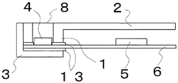
【0020】
前記デバイス4により生じた熱は、一部は孔8により大気に放熱するが、その大半はプリント基板6に伝わる。図1の断面図である図4に示すように、前記デバイス4の熱が最も伝わりやすいのは、デバイス4の真下に位置している下部放熱板3である。この下部放熱板3を略L字形状にし、空気に接する側面31を設けることにより、効率良く放熱することができる。なぜなら、側面31に面した大気が下方から上方に向かって対流するためである。
また、前記下部放熱板3を上部放熱板2にボルト7等で連結することにより、下部放熱板3の熱を上部放熱板2に伝えて、大気と接する面積の大きい上部放熱板2から効率的に放熱させることができる。
【0021】
プリント基板6とデバイス4および電子部品5のみにした状態で、デバイス4および電子部品5を連続して動作させた場合のデバイス4の温度は102度であったが、本実施形態に示した放熱構造では、デバイス4の温度は64.7度となり、約38度の温度低減効果があった。
尚、上部本熱板だけの場合のデバイス4の温度は75度であり、下部放熱板だけの場合のデバイス4の温度は74.7度であった。
【0022】
本実施例では、図3に示すように、デバイス4を用いた装置、例えば発光装置の筐体の一部として、上部放熱板2および下部放熱板3を用いているため、発光装置の小型軽量化および低コスト化を行うことができる。
また、前記上部放熱板2および下部放熱板3の材料として熱伝導率の高いアルミニウムまたは銅を採用することができる。アルミニウムについては、黒アルマイト処理を施すことにより、放熱効果を一層高めることができる。
【0023】
(第2実施形態)
図5は、第2実施形態に係るデバイスの放熱構造を示す。以下、第1実施形態との相違点のみ説明し、第1実施形態と同一の事項については、説明を省略する。
【0024】
図5に示すように、上部放熱板2とプリント基板6の間と、下部放熱板3とプリント基板6の間に放熱シート13を設けた点が第1実施形態との相違点である。該放熱シートは、柔らかく、放熱板とプリント基板の密着を向上させるものであれば良く、例えば、低硬度のシリコーンゴムを採用することができる。この放熱シート13を用いることにより、上部放熱板2、下部放熱板3とプリント基板6の密着が向上するため、第1実施形態に示した以上に放熱効果を高めることができる。
また、放熱シート13の代わりに、シリコーンを主成分とした放熱接着剤を採用しても同様の効果を得ることができる。
本実施形態においては、上部放熱板2、プリント基板6および下部放熱板3を固定するために、図1に示したボルト7に加えて、上部放熱板2、プリント基板6および下部放熱板3を貫通する上下方向の穴を2個あけ、ボルト等でとも締めすることが適している。なぜなら、前記放熱シートまたは放熱接着剤は弾性体であるため、上下方向にボルト等で締めることにより、上部放熱板2、プリント基板6および下部放熱板3との密着度が向上するからである。
【0025】
(第3実施形態)
図6は、第3実施形態に係るデバイスの放熱構造を示す。以下、第1実施形態との相違点のみ説明し、第1実施形態と同一の事項については、説明を省略する。
【0026】
図6に示すように、上部放熱板2に複数の凹部21と、下部放熱板3の側面31に複数の凹部32を設けることにより、上部放熱板2および下部放熱板3の表面積が大きくなり、放熱板自体がヒートシンクの働きをするため、さらに放熱効果を高めることができる。
ここで、下部放熱板3については、図7に示したように、前記した空気の対流ができやすいように凹部を上下方向に設ける方が、左右方向に設けるよりも放熱効果を大きくすることができる。
【0027】
(第4実施形態)
図7は、第4実施形態に係るデバイスの放熱構造を示す。以下、第1実施形態との相違点のみ説明し、第1実施形態と同一の事項については、説明を省略する。
【0028】
図7に示すように、上部放熱板2に複数のヒートシンク10を設けることにより、上部放熱板2表面積が実質的に大きくなり、放熱効果を大きくすることができる。
ヒートシンクは市販されているものを採用することができ、ヒートシンク10の下面に前記した放熱シートまたは放熱接着剤を付けることにより上部放熱板2に固定する。
尚、図示を省略したが、下部放熱板3の側面31にも同様にヒートシンクを貼り付けることにより、さらに放熱効果を向上させることができる。
【0029】
(第5実施形態)
図8および図9は、第5実施形態に係るデバイスの放熱構造を示す。以下、第1実施形態との相違点のみ説明し、第1実施形態と同一の事項については、説明を省略する。
【0030】
図8は、第1実施形態におけるプリント基板6を下方から見た斜視図であり、プリント基板6に伝わった熱を下部放熱板3に伝えやすいように、プリント基板6の裏面に銅箔ベタパターン11を設けたものである。
この銅箔ベタパターン11は、プリント基板6が下部放熱板3と密着する部分の面積よりも大きい方が適している。プリント基板6の裏面に配線パターンが無ければ、プリント基板7の全面を銅箔ベタパターンにしても良い。
【0031】
図9は、第1実施形態におけるプリント基板6を上方から見た斜視図であり、プリント基板6に伝わった熱を上部放熱板2に伝えやすいように、プリント基板6の表面に銅箔ベタパターン12を設けたものである。
図9では、放熱効率を上げるためにデバイス4の周囲を全て囲んだロ字状の銅箔ベタパターンを例示したが、電子部品5との配線パターンを設けるため、コ字状の銅箔ベタパターンにしても良い。図9に示したロ字状の銅箔ベタパターンの場合は、プリント基板6を多層にし、中間にある層の配線パターンを用いてデバイス4と電子部品5を電気的に接続することになる。
【0032】
図8および図9に示した銅箔ベタパターンを用いることにより、プリント基板6の熱の伝導を良くすることができる。また、プリント基板6の裏面全体に銅箔ベタパターンを設けた場合は、プリント基板自体も放熱機能を持たせることができるため、さらに放熱効率を向上させることができる。
また、銅箔ベタパターンの上にはレジストが無い方が放熱効果を高めることができる。
【0033】
(第6実施形態)
図10は、第6実施形態に係るデバイスの放熱構造を示す。以下、第1実施形態との相違点のみ説明し、第1実施形態と同一の事項については、説明を省略する。
【0034】
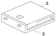
図10は、第6実施形態における放熱構造を上方から見た斜視図であり、下部放熱板3が略コ字形状である点が第1実施形態との相違点である。プリント基板6の裏面全体を銅箔ベタパターンにし、プリント基板6の裏面全体に放熱シートを貼り付けて下部放熱板3に密着させることにより、さらに放熱効果を高めることができる。
【0035】
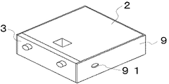
前記した実施例1〜6に示したデバイス4の放熱構造は、実際には、外部からのノイズによる影響を無くすため、図3に示した金属等の導電性のあるカバー9で囲った装置として使われることになる。各実施例においては、説明を容易にするため、カバー9の説明を省略した。
尚、カバー9には、装置内部の空気を大気と連通させるための孔91を少なくとも2つ設けることが好ましい。
【0036】
前記した発明の実施の形態は、説明のために例示したものであって、本発明としてはそれらに限定されるものではなく、特許請求の範囲、発明の詳細な説明および図面の記載から当業者が認識することができる本発明の技術的思想に反しない限り、変更および付加が可能である。
【0037】
例えば、図11に示すように、上部放熱板2が装置筐体の上面および側面になっても良い。
また、例えば、図12に示すように、上部放熱板2が凸部1を有する略T字形状であっても良い。該凸部1に、複数の孔8を設け、該孔8に複数のデバイス4を設けても良い。さらに、図示しないが、上部放熱板2の凸部1は複数であっても良い。
尚、実施例では、デバイスとして面発光素子を例示して説明したが、本発明はこれに限られることはなく、発熱する素子であれば適用可能であることは言うまでもない。
【0038】
【発明の効果】
デバイスの表面に直接放熱構造を取り付けることができないデバイスであっても、小型で安価に放熱することができる。
【図面の簡単な説明】
【図1】第1実施形態に係るデバイスの放熱構造を説明する斜視図である。
【図2】第1実施形態に係るデバイスの放熱構造を説明する斜視図である。
【図3】第1実施形態に係るデバイスの放熱構造を説明する斜視図である。
【図4】第1実施形態に係るデバイスの放熱構造を説明する断面図である。
【図5】第2実施形態に係るデバイスの放熱構造を説明する断面図である。
【図6】第3実施形態に係るデバイスの放熱構造を説明する斜視図である。
【図7】第4実施形態に係るデバイスの放熱構造を説明する斜視図である。
【図8】第5実施形態に係るデバイスの放熱構造を説明する斜視図である。
【図9】第5実施形態に係るデバイスの放熱構造を説明する斜視図である。
【図10】第6実施形態に係るデバイスの放熱構造を説明する斜視図である。
【図11】本発明に係る他の実施形態を説明する斜視図である。
【図12】本発明に係る他の実施形態を説明する斜視図である。
【符号の説明】
1 凸部
2 上部放熱板
3 下部放熱板
4 デバイス
5 電子部品
6 プリント基板
7 ボルト
8 孔
9 カバー
10 ヒートシンク
11 銅箔ベタパターン
12 銅箔ベタパターン
13 放熱シート[0001]
TECHNICAL FIELD OF THE INVENTION
The present invention relates to a heat dissipation structure of an electronic component, and more particularly, to a heat dissipation structure of a device for dissipating heat from a printed circuit board on which the device is mounted when a heat sink cannot be directly attached to the surface of the device to dissipate heat.
[0002]
[Prior art]
The following four methods are mainly used for heat radiation from a device mounted on a printed circuit board.
(1) A method in which heat is directly released from the surface of the device to the atmosphere.
(2) A method in which heat is conducted from the surface of the device to a metal or the like which is a good conductor of heat to release heat to the atmosphere (for example, see Patent Document 1).
(3) A method in which heat is conducted to a printed board on which devices are mounted, and heat is directly released from the printed board to the atmosphere.
(4) A method of radiating heat from the device surface to release heat to the atmosphere.
[0003]
However, each of the above methods has the following problems.
The above (1) has a problem that a heat dissipation effect cannot be expected when the fluidity of the air is poor in a narrow space in the device housing.
Regarding the above (2), heat can be effectively dissipated by attaching a heat sink or the like to the surface of the device. However, when the device surface is a light emitting surface or the like, it is necessary to release heat directly from a metal or the like. There is a problem that a special housing and a metal case are required (for example, see Patent Document 2).
In addition, the above (3) has a problem that the thermal conductivity of the printed circuit board is generally low, and particularly in the case of a thin plate or a low-layer structure, it cannot be expected as a good heat conductor.
Furthermore, the above (4) has a problem that heat transfer due to radiation is small from a glossy surface because it is greatly affected by the emissivity of the device surface.
[0004]
In order to cope with the above-mentioned problem, a method of enlarging a casing space, using forced air cooling such as a fan, or mounting an electronic cooler under a substrate to dissipate heat is generally used (for example, see
[0005]
[Patent Document 1]
JP-A-6-196598 [Patent Document 2]
JP-A-5-3330 [Patent Document 3]
JP-A-5-95062 [Patent Document 4]
JP-A-7-287130
[Problems to be solved by the invention]
However, when the space of the device housing is enlarged, there is a problem that the housing itself becomes large and heavy, and the cost increases. Similarly, when a forced cooling device such as a fan or an electronic cooler is used, it is necessary to increase the space of the device housing, and there is a problem of large size, high weight, and high cost.
[0007]
In addition, when the surface of the device is a light-emitting surface or the like, there is a problem that a special housing and a metal case surrounding substantially the entire device are required to radiate the heat of the device.
[0008]
SUMMARY OF THE INVENTION It is an object of the present invention to provide a heat radiating structure that can radiate heat from a device in a small, low-weight, and inexpensive manner while the surface of the device is in contact with the atmosphere in order to solve such a problem.
[0009]
[Means for Solving the Problems]
The heat dissipation structure of the device according to
[0010]
The heat radiating structure of the device according to
[0011]
The heat dissipation structure of the device according to
[0012]
According to a fourth aspect of the present invention, in the heat radiation structure of the device according to the first aspect, the upper heat radiation plate is a part or all of an upper surface and a side surface of the device housing, and the lower heat radiation plate is a part of the device housing. It is part or all of the lower surface of the body. With this configuration, the upper heat sink and the lower heat sink become the housing of the device as they are, so that the cost of the device housing can be reduced, that is, the cost of the device in which the device is mounted can be reduced.
[0013]
According to a fifth aspect of the present invention, in the heat dissipation structure of the device according to the first aspect, the material of the upper heatsink and the lower heatsink is copper or aluminum subjected to black alumite treatment. . With this configuration, heat transmitted from the device can be efficiently released to the atmosphere. When the device with this heat dissipation structure is mounted on a base made of metal, etc., since the lower heat sink is made of copper or aluminum treated with black alumite, the heat transferred from the device is transferred to the lower heat sink. Can escape to the base.
[0014]
The heat radiation structure of the device according to
[0015]
According to a seventh aspect of the present invention, in the heat dissipation structure of the device according to the first aspect, a heat sink is attached to the upper heat sink and / or the lower heat sink. With this configuration, the surface area of the upper radiator plate and / or the lower radiator plate increases, so that heat accumulated in the upper radiator plate and / or the lower radiator plate can be easily released to the atmosphere.
[0016]
The heat dissipation structure of the device according to
[0017]
BEST MODE FOR CARRYING OUT THE INVENTION
Hereinafter, embodiments of the present invention will be described in detail with reference to the drawings.
[0018]
(1st Embodiment)
FIG. 1 is a perspective view showing a heat dissipation structure according to the first embodiment, and FIG. 2 is an exploded view thereof. As shown in FIGS. 1 and 2, a printed
The
[0019]
The
[0020]
Part of the heat generated by the
Further, by connecting the
[0021]
When the
The temperature of the
[0022]
In this embodiment, as shown in FIG. 3, since the
Further, aluminum or copper having high thermal conductivity can be adopted as a material of the
[0023]
(2nd Embodiment)
FIG. 5 shows a heat dissipation structure of the device according to the second embodiment. Hereinafter, only the differences from the first embodiment will be described, and the description of the same items as the first embodiment will be omitted.
[0024]
As shown in FIG. 5, a difference from the first embodiment is that a heat radiating sheet 13 is provided between the upper
The same effect can be obtained by using a heat-radiating adhesive containing silicone as a main component instead of the heat-radiating sheet 13.
In this embodiment, in order to fix the
[0025]
(Third embodiment)
FIG. 6 shows a heat dissipation structure of the device according to the third embodiment. Hereinafter, only the differences from the first embodiment will be described, and the description of the same items as the first embodiment will be omitted.
[0026]
As shown in FIG. 6, by providing a plurality of recesses 21 on the
Here, as for the
[0027]
(Fourth embodiment)
FIG. 7 shows a heat dissipation structure of the device according to the fourth embodiment. Hereinafter, only the differences from the first embodiment will be described, and the description of the same items as the first embodiment will be omitted.
[0028]
As shown in FIG. 7, by providing the plurality of heat sinks 10 on the
A commercially available heat sink can be used, and the heat sink 10 is fixed to the upper
Although not shown, a heat sink can be similarly attached to the side surface 31 of the
[0029]
(Fifth embodiment)
8 and 9 show a heat dissipation structure of the device according to the fifth embodiment. Hereinafter, only the differences from the first embodiment will be described, and the description of the same items as the first embodiment will be omitted.
[0030]
FIG. 8 is a perspective view of the printed
The copper foil solid pattern 11 is preferably larger than the area of the portion where the printed
[0031]
FIG. 9 is a perspective view of the printed
In FIG. 9, a square-shaped copper foil solid pattern surrounding the entire periphery of the
[0032]
By using the copper foil solid pattern shown in FIGS. 8 and 9, heat conduction of the printed
Further, the absence of the resist on the copper foil solid pattern can enhance the heat radiation effect.
[0033]
(Sixth embodiment)
FIG. 10 shows a heat dissipation structure of the device according to the sixth embodiment. Hereinafter, only the differences from the first embodiment will be described, and the description of the same items as the first embodiment will be omitted.
[0034]
FIG. 10 is a perspective view of the heat radiating structure according to the sixth embodiment as viewed from above, and is different from the first embodiment in that the lower
[0035]
The heat dissipation structure of the
Preferably, the
[0036]
The above-described embodiments of the present invention have been described by way of example only, and the present invention is not limited to these embodiments. Those skilled in the art will understand from the claims, the detailed description of the invention, and the drawings. Modifications and additions are possible without departing from the technical idea of the present invention that can be recognized.
[0037]
For example, as shown in FIG. 11, the
Further, for example, as shown in FIG. 12, the
In the embodiments, the surface light emitting element is described as an example of the device. However, the present invention is not limited to this, and it goes without saying that the present invention is applicable to any element that generates heat.
[0038]
【The invention's effect】
Even a device in which the heat radiation structure cannot be directly attached to the surface of the device can be radiated at a small size and at low cost.
[Brief description of the drawings]
FIG. 1 is a perspective view illustrating a heat dissipation structure of a device according to a first embodiment.
FIG. 2 is a perspective view illustrating a heat dissipation structure of the device according to the first embodiment.
FIG. 3 is a perspective view illustrating a heat dissipation structure of the device according to the first embodiment.
FIG. 4 is a cross-sectional view illustrating a heat dissipation structure of the device according to the first embodiment.
FIG. 5 is a cross-sectional view illustrating a heat dissipation structure of a device according to a second embodiment.
FIG. 6 is a perspective view illustrating a heat dissipation structure of a device according to a third embodiment.
FIG. 7 is a perspective view illustrating a heat dissipation structure of a device according to a fourth embodiment.
FIG. 8 is a perspective view illustrating a heat dissipation structure of a device according to a fifth embodiment.
FIG. 9 is a perspective view illustrating a heat dissipation structure of a device according to a fifth embodiment.
FIG. 10 is a perspective view illustrating a heat dissipation structure of a device according to a sixth embodiment.
FIG. 11 is a perspective view illustrating another embodiment according to the present invention.
FIG. 12 is a perspective view illustrating another embodiment according to the present invention.
[Explanation of symbols]
DESCRIPTION OF
Claims (8)
前記デバイスを取り囲むように大気と連通する孔が設けられた凸部を有する上部放熱板と、
断面略L字形状または略コ字形状の下部放熱板とを設け、
前記凸部と前記下部放熱板とで前記プリント基板を密着するように挟み込み、
前記上部放熱板と前記下部放熱板を連結したことを特徴とするデバイスの放熱構造。In the heat dissipation structure of the device mounted on the printed circuit board, the back surface of the device is opposed to the surface of the printed circuit board, and the surface of the device is in contact with the atmosphere,
An upper heat sink having a convex portion provided with a hole communicating with the atmosphere to surround the device,
A lower heat sink having a substantially L-shaped or substantially U-shaped cross section;
Sandwiching the printed circuit board in close contact with the convex portion and the lower heat sink,
A heat radiation structure for a device, wherein the upper heat radiation plate and the lower heat radiation plate are connected.
前記上部放熱板と前記プリント基板の間、および/または前記下部放熱板と前記プリント基板の間に、放熱シートを設けたことを特徴とするデバイスの放熱構造。The heat dissipation structure of the device according to claim 1,
A heat dissipation structure for a device, wherein a heat dissipation sheet is provided between the upper heat sink and the printed board and / or between the lower heat sink and the printed board.
前記上部放熱板が装置筐体の上面の一部または全部となり、
前記下部放熱板が前記装置筐体の下面および側面の一部または全部となることを特徴とするデバイスの放熱構造。The device for radiating heat according to claim 1,
The upper heat sink is part or all of the upper surface of the device housing,
A heat dissipation structure for a device, wherein the lower heat dissipation plate forms part or all of a lower surface and side surfaces of the apparatus housing.
前記上部放熱板が装置筐体の上面および側面の一部または全部となり、
前記下部放熱板が前記装置筐体の下面の一部または全部となることを特徴とするデバイスの放熱構造。The device for radiating heat according to claim 1,
The upper heat sink is part or all of the upper surface and side surfaces of the device housing,
The heat radiating structure of a device, wherein the lower heat radiating plate is part or all of a lower surface of the device housing.
前記上部放熱板および前記下部放熱板の材質は、銅または黒アルマイト処理されたアルミニウムであることを特徴とするデバイスの放熱構造。The heat dissipation structure of the device according to claim 1,
The heat radiating structure of the device, wherein a material of the upper heat radiating plate and the lower heat radiating plate is copper or aluminum treated with black alumite.
前記プリント基板が前記凸部と密着する部分および/または前記プリント基板が前記下部放熱板と密着する部分において、前記プリント基板の表面および/または裏面に銅箔ベタパターンが設けられていることを特徴とするデバイスの放熱構造。The heat dissipation structure of the device according to claim 1,
A solid copper foil pattern is provided on a front surface and / or a back surface of the printed circuit board in a portion where the printed circuit board is in close contact with the convex portion and / or in a portion where the printed circuit board is in close contact with the lower heat sink. The heat dissipation structure of the device.
前記上部放熱板および/または前記下部放熱板にヒートシンクが取り付けられていることを特徴とするデバイスの放熱構造。The heat dissipation structure of the device according to claim 1,
A heat dissipation structure for a device, wherein a heat sink is attached to the upper heat sink and / or the lower heat sink.
前記上部放熱板および/または前記下部放熱板に複数の凹部を設け、ヒートシンクの機能を持たせたことを特徴とするデバイスの放熱構造。The heat dissipation structure of the device according to claim 1,
A heat dissipation structure for a device, wherein a plurality of recesses are provided in the upper heat sink and / or the lower heat sink to function as a heat sink.
Priority Applications (1)
| Application Number | Priority Date | Filing Date | Title |
|---|---|---|---|
| JP2002369217A JP2004200533A (en) | 2002-12-20 | 2002-12-20 | Heat radiation structure of device |
Applications Claiming Priority (1)
| Application Number | Priority Date | Filing Date | Title |
|---|---|---|---|
| JP2002369217A JP2004200533A (en) | 2002-12-20 | 2002-12-20 | Heat radiation structure of device |
Publications (1)
| Publication Number | Publication Date |
|---|---|
| JP2004200533A true JP2004200533A (en) | 2004-07-15 |
Family
ID=32765499
Family Applications (1)
| Application Number | Title | Priority Date | Filing Date |
|---|---|---|---|
| JP2002369217A Abandoned JP2004200533A (en) | 2002-12-20 | 2002-12-20 | Heat radiation structure of device |
Country Status (1)
| Country | Link |
|---|---|
| JP (1) | JP2004200533A (en) |
Cited By (7)
| Publication number | Priority date | Publication date | Assignee | Title |
|---|---|---|---|---|
| JP2007104573A (en) * | 2005-10-07 | 2007-04-19 | Olympus Corp | Cooling imaging unit and imaging apparatus mounting the imaging cooling unit therein |
| JP2008293549A (en) * | 2007-05-22 | 2008-12-04 | Teac Corp | Optical disk unit |
| CN102427655A (en) * | 2011-08-31 | 2012-04-25 | 昆山锦泰电子器材有限公司 | Radiating fin structure |
| JPWO2013046416A1 (en) * | 2011-09-29 | 2015-03-26 | 富士通株式会社 | Optical module |
| KR20150090690A (en) * | 2014-01-29 | 2015-08-06 | 엘지이노텍 주식회사 | PRINTED CIRCUIT BOARD AND luminous device INCLUDING THE SAME |
| KR101855996B1 (en) * | 2016-02-02 | 2018-05-09 | 박재성 | Slim type main computer |
| US20230304655A1 (en) * | 2020-08-13 | 2023-09-28 | Lumileds Llc | Electronic device, light emitting device and method for manufacturing an electronic device |
-
2002
- 2002-12-20 JP JP2002369217A patent/JP2004200533A/en not_active Abandoned
Cited By (8)
| Publication number | Priority date | Publication date | Assignee | Title |
|---|---|---|---|---|
| JP2007104573A (en) * | 2005-10-07 | 2007-04-19 | Olympus Corp | Cooling imaging unit and imaging apparatus mounting the imaging cooling unit therein |
| JP2008293549A (en) * | 2007-05-22 | 2008-12-04 | Teac Corp | Optical disk unit |
| CN102427655A (en) * | 2011-08-31 | 2012-04-25 | 昆山锦泰电子器材有限公司 | Radiating fin structure |
| JPWO2013046416A1 (en) * | 2011-09-29 | 2015-03-26 | 富士通株式会社 | Optical module |
| KR20150090690A (en) * | 2014-01-29 | 2015-08-06 | 엘지이노텍 주식회사 | PRINTED CIRCUIT BOARD AND luminous device INCLUDING THE SAME |
| KR102148846B1 (en) * | 2014-01-29 | 2020-08-27 | 엘지이노텍 주식회사 | PRINTED CIRCUIT BOARD AND luminous device INCLUDING THE SAME |
| KR101855996B1 (en) * | 2016-02-02 | 2018-05-09 | 박재성 | Slim type main computer |
| US20230304655A1 (en) * | 2020-08-13 | 2023-09-28 | Lumileds Llc | Electronic device, light emitting device and method for manufacturing an electronic device |
Similar Documents
| Publication | Publication Date | Title |
|---|---|---|
| TWI495423B (en) | Thermal module and electronic device incorporating the same | |
| JP2004200533A (en) | Heat radiation structure of device | |
| JP4438526B2 (en) | Power component cooling system | |
| TW201201000A (en) | Heat dissipation apparatus | |
| JP2001111237A (en) | Multilayer printed board and electronic apparatus | |
| JPH08204070A (en) | Electronic part cooling structure | |
| JP2012199354A (en) | Electronic control device | |
| JPH07106721A (en) | Printed circuit board and heat radiating method | |
| JP2004214429A (en) | Heat radiation structure of laminated printed circuit board | |
| JP4469101B2 (en) | Electronic circuit device having heat dissipation structure | |
| JPH1098287A (en) | Cooler for circuit board module and portable electronic equipment having the cooler | |
| JP2005057070A (en) | Heat radiating structure of electronic equipment | |
| JP2001230580A (en) | Electronic apparatus with module board | |
| KR20030073422A (en) | Plasma display unit | |
| JPH10340138A (en) | Electronic device | |
| JPH11220278A (en) | Heat dissipating structure of heat releasing part | |
| KR100264370B1 (en) | Heat sink | |
| JP2912268B2 (en) | Method and apparatus for radiating electronic components | |
| JP2003258465A (en) | Electronic circuit unit | |
| JP2007281371A (en) | Heat dissipating structure for electronic equipment | |
| JP2003243860A (en) | Electronic appliance | |
| JP2001244672A (en) | Electronic component cooling device | |
| JPH09321471A (en) | Heat radiating device for electronic component | |
| JP2003017634A (en) | Semiconductor module | |
| JPH0660166U (en) | Heat dissipation device for electronic components |
Legal Events
| Date | Code | Title | Description |
|---|---|---|---|
| A621 | Written request for application examination |
Effective date: 20050823 Free format text: JAPANESE INTERMEDIATE CODE: A621 |
|
| A762 | Written abandonment of application |
Effective date: 20070510 Free format text: JAPANESE INTERMEDIATE CODE: A762 |