JP2004200377A - Semiconductor memory element, semiconductor memory device and its manufacturing method - Google Patents
Semiconductor memory element, semiconductor memory device and its manufacturing method Download PDFInfo
- Publication number
- JP2004200377A JP2004200377A JP2002366600A JP2002366600A JP2004200377A JP 2004200377 A JP2004200377 A JP 2004200377A JP 2002366600 A JP2002366600 A JP 2002366600A JP 2002366600 A JP2002366600 A JP 2002366600A JP 2004200377 A JP2004200377 A JP 2004200377A
- Authority
- JP
- Japan
- Prior art keywords
- semiconductor
- semiconductor memory
- channel region
- film
- active layer
- Prior art date
- Legal status (The legal status is an assumption and is not a legal conclusion. Google has not performed a legal analysis and makes no representation as to the accuracy of the status listed.)
- Granted
Links
- 239000004065 semiconductor Substances 0.000 title claims abstract description 414
- 238000004519 manufacturing process Methods 0.000 title claims abstract description 32
- 239000000758 substrate Substances 0.000 claims abstract description 113
- 230000015654 memory Effects 0.000 claims abstract description 110
- 229910052751 metal Inorganic materials 0.000 claims abstract description 42
- 238000000034 method Methods 0.000 claims abstract description 41
- 238000010438 heat treatment Methods 0.000 claims abstract description 28
- 238000003860 storage Methods 0.000 claims description 54
- 239000013078 crystal Substances 0.000 claims description 44
- 239000002184 metal Substances 0.000 claims description 40
- 239000012535 impurity Substances 0.000 claims description 35
- 238000002425 crystallisation Methods 0.000 claims description 20
- 230000008025 crystallization Effects 0.000 claims description 20
- 230000003746 surface roughness Effects 0.000 claims description 18
- 230000001678 irradiating effect Effects 0.000 claims description 12
- 239000004033 plastic Substances 0.000 claims description 12
- 229920003023 plastic Polymers 0.000 claims description 12
- 230000004931 aggregating effect Effects 0.000 claims description 10
- 239000011159 matrix material Substances 0.000 claims description 8
- 239000000919 ceramic Substances 0.000 claims description 5
- 229910052732 germanium Inorganic materials 0.000 claims description 4
- 229910052802 copper Inorganic materials 0.000 claims description 3
- 229910052737 gold Inorganic materials 0.000 claims description 3
- 229910052759 nickel Inorganic materials 0.000 claims description 3
- 229910052763 palladium Inorganic materials 0.000 claims description 3
- 229910052697 platinum Inorganic materials 0.000 claims description 3
- 229910052718 tin Inorganic materials 0.000 claims description 3
- 229910052742 iron Inorganic materials 0.000 claims description 2
- 238000010030 laminating Methods 0.000 claims description 2
- 230000010355 oscillation Effects 0.000 abstract description 23
- 230000008569 process Effects 0.000 abstract description 8
- 230000000694 effects Effects 0.000 abstract description 5
- 239000010408 film Substances 0.000 description 203
- 239000010410 layer Substances 0.000 description 42
- 238000012545 processing Methods 0.000 description 18
- 239000010409 thin film Substances 0.000 description 12
- 229910044991 metal oxide Inorganic materials 0.000 description 11
- 150000004706 metal oxides Chemical class 0.000 description 11
- 230000002093 peripheral effect Effects 0.000 description 11
- VYPSYNLAJGMNEJ-UHFFFAOYSA-N silicon dioxide Inorganic materials O=[Si]=O VYPSYNLAJGMNEJ-UHFFFAOYSA-N 0.000 description 11
- 239000011241 protective layer Substances 0.000 description 10
- XUIMIQQOPSSXEZ-UHFFFAOYSA-N Silicon Chemical compound [Si] XUIMIQQOPSSXEZ-UHFFFAOYSA-N 0.000 description 9
- 239000000853 adhesive Substances 0.000 description 9
- 230000001070 adhesive effect Effects 0.000 description 9
- PXHVJJICTQNCMI-UHFFFAOYSA-N nickel Substances [Ni] PXHVJJICTQNCMI-UHFFFAOYSA-N 0.000 description 9
- 229910052710 silicon Inorganic materials 0.000 description 9
- 239000010703 silicon Substances 0.000 description 9
- 238000005247 gettering Methods 0.000 description 8
- 238000004544 sputter deposition Methods 0.000 description 8
- 229910052581 Si3N4 Inorganic materials 0.000 description 7
- 239000002585 base Substances 0.000 description 7
- 239000003054 catalyst Substances 0.000 description 7
- HQVNEWCFYHHQES-UHFFFAOYSA-N silicon nitride Chemical compound N12[Si]34N5[Si]62N3[Si]51N64 HQVNEWCFYHHQES-UHFFFAOYSA-N 0.000 description 7
- 230000005684 electric field Effects 0.000 description 6
- 238000005530 etching Methods 0.000 description 6
- 229910052814 silicon oxide Inorganic materials 0.000 description 6
- 238000000137 annealing Methods 0.000 description 5
- 238000000089 atomic force micrograph Methods 0.000 description 5
- 238000010586 diagram Methods 0.000 description 5
- 239000007789 gas Substances 0.000 description 5
- 239000011521 glass Substances 0.000 description 5
- 239000011229 interlayer Substances 0.000 description 5
- 230000003287 optical effect Effects 0.000 description 5
- 238000005268 plasma chemical vapour deposition Methods 0.000 description 5
- 239000010453 quartz Substances 0.000 description 5
- 239000010936 titanium Substances 0.000 description 5
- 238000003917 TEM image Methods 0.000 description 4
- 230000005856 abnormality Effects 0.000 description 4
- 230000015572 biosynthetic process Effects 0.000 description 4
- 230000006872 improvement Effects 0.000 description 4
- 230000010365 information processing Effects 0.000 description 4
- 230000010354 integration Effects 0.000 description 4
- 239000004973 liquid crystal related substance Substances 0.000 description 4
- 239000000463 material Substances 0.000 description 4
- KDLHZDBZIXYQEI-UHFFFAOYSA-N palladium Substances [Pd] KDLHZDBZIXYQEI-UHFFFAOYSA-N 0.000 description 4
- BASFCYQUMIYNBI-UHFFFAOYSA-N platinum Substances [Pt] BASFCYQUMIYNBI-UHFFFAOYSA-N 0.000 description 4
- 239000007787 solid Substances 0.000 description 4
- 238000012546 transfer Methods 0.000 description 4
- LEVVHYCKPQWKOP-UHFFFAOYSA-N [Si].[Ge] Chemical compound [Si].[Ge] LEVVHYCKPQWKOP-UHFFFAOYSA-N 0.000 description 3
- 238000006243 chemical reaction Methods 0.000 description 3
- 239000010949 copper Substances 0.000 description 3
- 238000009792 diffusion process Methods 0.000 description 3
- 239000010931 gold Substances 0.000 description 3
- 238000002347 injection Methods 0.000 description 3
- 239000007924 injection Substances 0.000 description 3
- 238000005499 laser crystallization Methods 0.000 description 3
- 238000009832 plasma treatment Methods 0.000 description 3
- 229910021420 polycrystalline silicon Inorganic materials 0.000 description 3
- 229920005989 resin Polymers 0.000 description 3
- 239000011347 resin Substances 0.000 description 3
- 239000011135 tin Substances 0.000 description 3
- 229910052719 titanium Inorganic materials 0.000 description 3
- WFKWXMTUELFFGS-UHFFFAOYSA-N tungsten Chemical compound [W] WFKWXMTUELFFGS-UHFFFAOYSA-N 0.000 description 3
- 229910052721 tungsten Inorganic materials 0.000 description 3
- 239000010937 tungsten Substances 0.000 description 3
- XLYOFNOQVPJJNP-UHFFFAOYSA-N water Substances O XLYOFNOQVPJJNP-UHFFFAOYSA-N 0.000 description 3
- XKRFYHLGVUSROY-UHFFFAOYSA-N Argon Chemical compound [Ar] XKRFYHLGVUSROY-UHFFFAOYSA-N 0.000 description 2
- 239000004593 Epoxy Substances 0.000 description 2
- KRHYYFGTRYWZRS-UHFFFAOYSA-N Fluorane Chemical compound F KRHYYFGTRYWZRS-UHFFFAOYSA-N 0.000 description 2
- 229910052688 Gadolinium Inorganic materials 0.000 description 2
- GYHNNYVSQQEPJS-UHFFFAOYSA-N Gallium Chemical compound [Ga] GYHNNYVSQQEPJS-UHFFFAOYSA-N 0.000 description 2
- 229910052689 Holmium Inorganic materials 0.000 description 2
- OAKJQQAXSVQMHS-UHFFFAOYSA-N Hydrazine Chemical compound NN OAKJQQAXSVQMHS-UHFFFAOYSA-N 0.000 description 2
- VEXZGXHMUGYJMC-UHFFFAOYSA-N Hydrochloric acid Chemical compound Cl VEXZGXHMUGYJMC-UHFFFAOYSA-N 0.000 description 2
- MHAJPDPJQMAIIY-UHFFFAOYSA-N Hydrogen peroxide Chemical compound OO MHAJPDPJQMAIIY-UHFFFAOYSA-N 0.000 description 2
- ZOKXTWBITQBERF-UHFFFAOYSA-N Molybdenum Chemical compound [Mo] ZOKXTWBITQBERF-UHFFFAOYSA-N 0.000 description 2
- 229910052779 Neodymium Inorganic materials 0.000 description 2
- XYFCBTPGUUZFHI-UHFFFAOYSA-N Phosphine Chemical compound P XYFCBTPGUUZFHI-UHFFFAOYSA-N 0.000 description 2
- OAICVXFJPJFONN-UHFFFAOYSA-N Phosphorus Chemical compound [P] OAICVXFJPJFONN-UHFFFAOYSA-N 0.000 description 2
- 239000004743 Polypropylene Substances 0.000 description 2
- 229910000577 Silicon-germanium Inorganic materials 0.000 description 2
- QAOWNCQODCNURD-UHFFFAOYSA-N Sulfuric acid Chemical compound OS(O)(=O)=O QAOWNCQODCNURD-UHFFFAOYSA-N 0.000 description 2
- RTAQQCXQSZGOHL-UHFFFAOYSA-N Titanium Chemical compound [Ti] RTAQQCXQSZGOHL-UHFFFAOYSA-N 0.000 description 2
- 229910052783 alkali metal Inorganic materials 0.000 description 2
- 150000001340 alkali metals Chemical class 0.000 description 2
- 229910052784 alkaline earth metal Inorganic materials 0.000 description 2
- 150000001342 alkaline earth metals Chemical class 0.000 description 2
- 229910045601 alloy Inorganic materials 0.000 description 2
- 239000000956 alloy Substances 0.000 description 2
- LFVGISIMTYGQHF-UHFFFAOYSA-N ammonium dihydrogen phosphate Chemical compound [NH4+].OP(O)([O-])=O LFVGISIMTYGQHF-UHFFFAOYSA-N 0.000 description 2
- 229910000387 ammonium dihydrogen phosphate Inorganic materials 0.000 description 2
- 239000007864 aqueous solution Substances 0.000 description 2
- 229910052785 arsenic Inorganic materials 0.000 description 2
- RQNWIZPPADIBDY-UHFFFAOYSA-N arsenic atom Chemical compound [As] RQNWIZPPADIBDY-UHFFFAOYSA-N 0.000 description 2
- 239000012298 atmosphere Substances 0.000 description 2
- QVGXLLKOCUKJST-UHFFFAOYSA-N atomic oxygen Chemical compound [O] QVGXLLKOCUKJST-UHFFFAOYSA-N 0.000 description 2
- 238000007796 conventional method Methods 0.000 description 2
- 229910021419 crystalline silicon Inorganic materials 0.000 description 2
- 238000009826 distribution Methods 0.000 description 2
- 238000001704 evaporation Methods 0.000 description 2
- UIWYJDYFSGRHKR-UHFFFAOYSA-N gadolinium atom Chemical compound [Gd] UIWYJDYFSGRHKR-UHFFFAOYSA-N 0.000 description 2
- 229910052733 gallium Inorganic materials 0.000 description 2
- 239000002223 garnet Substances 0.000 description 2
- GNPVGFCGXDBREM-UHFFFAOYSA-N germanium atom Chemical compound [Ge] GNPVGFCGXDBREM-UHFFFAOYSA-N 0.000 description 2
- 239000002784 hot electron Substances 0.000 description 2
- XEEYBQQBJWHFJM-UHFFFAOYSA-N iron Substances [Fe] XEEYBQQBJWHFJM-UHFFFAOYSA-N 0.000 description 2
- 230000033001 locomotion Effects 0.000 description 2
- 229910052750 molybdenum Inorganic materials 0.000 description 2
- 239000011733 molybdenum Substances 0.000 description 2
- 235000019837 monoammonium phosphate Nutrition 0.000 description 2
- 235000019796 monopotassium phosphate Nutrition 0.000 description 2
- 239000012299 nitrogen atmosphere Substances 0.000 description 2
- 230000003647 oxidation Effects 0.000 description 2
- 238000007254 oxidation reaction Methods 0.000 description 2
- 230000001590 oxidative effect Effects 0.000 description 2
- 239000001301 oxygen Substances 0.000 description 2
- 229910052760 oxygen Inorganic materials 0.000 description 2
- 229910052698 phosphorus Inorganic materials 0.000 description 2
- 239000011574 phosphorus Substances 0.000 description 2
- -1 polypropylene Polymers 0.000 description 2
- 229920001155 polypropylene Polymers 0.000 description 2
- 229910000679 solder Inorganic materials 0.000 description 2
- 229920003002 synthetic resin Polymers 0.000 description 2
- 239000000057 synthetic resin Substances 0.000 description 2
- 229910052715 tantalum Inorganic materials 0.000 description 2
- GUVRBAGPIYLISA-UHFFFAOYSA-N tantalum atom Chemical compound [Ta] GUVRBAGPIYLISA-UHFFFAOYSA-N 0.000 description 2
- 238000002834 transmittance Methods 0.000 description 2
- NIXOWILDQLNWCW-UHFFFAOYSA-M Acrylate Chemical compound [O-]C(=O)C=C NIXOWILDQLNWCW-UHFFFAOYSA-M 0.000 description 1
- ZOXJGFHDIHLPTG-UHFFFAOYSA-N Boron Chemical compound [B] ZOXJGFHDIHLPTG-UHFFFAOYSA-N 0.000 description 1
- 229910052684 Cerium Inorganic materials 0.000 description 1
- RYGMFSIKBFXOCR-UHFFFAOYSA-N Copper Chemical compound [Cu] RYGMFSIKBFXOCR-UHFFFAOYSA-N 0.000 description 1
- 229910052691 Erbium Inorganic materials 0.000 description 1
- UFHFLCQGNIYNRP-UHFFFAOYSA-N Hydrogen Chemical compound [H][H] UFHFLCQGNIYNRP-UHFFFAOYSA-N 0.000 description 1
- GRYLNZFGIOXLOG-UHFFFAOYSA-N Nitric acid Chemical compound O[N+]([O-])=O GRYLNZFGIOXLOG-UHFFFAOYSA-N 0.000 description 1
- CBENFWSGALASAD-UHFFFAOYSA-N Ozone Chemical compound [O-][O+]=O CBENFWSGALASAD-UHFFFAOYSA-N 0.000 description 1
- 239000004697 Polyetherimide Substances 0.000 description 1
- 239000004642 Polyimide Substances 0.000 description 1
- 239000004721 Polyphenylene oxide Substances 0.000 description 1
- 239000004734 Polyphenylene sulfide Substances 0.000 description 1
- 239000004954 Polyphthalamide Substances 0.000 description 1
- 229910004298 SiO 2 Inorganic materials 0.000 description 1
- UCKMPCXJQFINFW-UHFFFAOYSA-N Sulphide Chemical compound [S-2] UCKMPCXJQFINFW-UHFFFAOYSA-N 0.000 description 1
- 229910052775 Thulium Inorganic materials 0.000 description 1
- ATJFFYVFTNAWJD-UHFFFAOYSA-N Tin Chemical compound [Sn] ATJFFYVFTNAWJD-UHFFFAOYSA-N 0.000 description 1
- PILOURHZNVHRME-UHFFFAOYSA-N [Na].[Ba] Chemical compound [Na].[Ba] PILOURHZNVHRME-UHFFFAOYSA-N 0.000 description 1
- 230000002159 abnormal effect Effects 0.000 description 1
- LPQOADBMXVRBNX-UHFFFAOYSA-N ac1ldcw0 Chemical group Cl.C1CN(C)CCN1C1=C(F)C=C2C(=O)C(C(O)=O)=CN3CCSC1=C32 LPQOADBMXVRBNX-UHFFFAOYSA-N 0.000 description 1
- MQRWBMAEBQOWAF-UHFFFAOYSA-N acetic acid;nickel Chemical compound [Ni].CC(O)=O.CC(O)=O MQRWBMAEBQOWAF-UHFFFAOYSA-N 0.000 description 1
- 230000003213 activating effect Effects 0.000 description 1
- 230000004913 activation Effects 0.000 description 1
- 230000002411 adverse Effects 0.000 description 1
- 238000004220 aggregation Methods 0.000 description 1
- 230000002776 aggregation Effects 0.000 description 1
- 150000001298 alcohols Chemical class 0.000 description 1
- 239000012670 alkaline solution Substances 0.000 description 1
- 239000005407 aluminoborosilicate glass Substances 0.000 description 1
- 229910021417 amorphous silicon Inorganic materials 0.000 description 1
- 229910052786 argon Inorganic materials 0.000 description 1
- 229910052788 barium Inorganic materials 0.000 description 1
- DSAJWYNOEDNPEQ-UHFFFAOYSA-N barium atom Chemical compound [Ba] DSAJWYNOEDNPEQ-UHFFFAOYSA-N 0.000 description 1
- 230000006399 behavior Effects 0.000 description 1
- 230000008901 benefit Effects 0.000 description 1
- 230000005540 biological transmission Effects 0.000 description 1
- 229910052796 boron Inorganic materials 0.000 description 1
- 239000005388 borosilicate glass Substances 0.000 description 1
- AQCDIIAORKRFCD-UHFFFAOYSA-N cadmium selenide Chemical compound [Cd]=[Se] AQCDIIAORKRFCD-UHFFFAOYSA-N 0.000 description 1
- UHYPYGJEEGLRJD-UHFFFAOYSA-N cadmium(2+);selenium(2-) Chemical compound [Se-2].[Cd+2] UHYPYGJEEGLRJD-UHFFFAOYSA-N 0.000 description 1
- 229910052804 chromium Inorganic materials 0.000 description 1
- 238000004140 cleaning Methods 0.000 description 1
- 239000011248 coating agent Substances 0.000 description 1
- 238000000576 coating method Methods 0.000 description 1
- 229910017052 cobalt Inorganic materials 0.000 description 1
- 239000010941 cobalt Substances 0.000 description 1
- GUTLYIVDDKVIGB-UHFFFAOYSA-N cobalt atom Chemical compound [Co] GUTLYIVDDKVIGB-UHFFFAOYSA-N 0.000 description 1
- 239000012141 concentrate Substances 0.000 description 1
- 230000007423 decrease Effects 0.000 description 1
- 238000001514 detection method Methods 0.000 description 1
- 230000006866 deterioration Effects 0.000 description 1
- 238000011161 development Methods 0.000 description 1
- 230000006870 function Effects 0.000 description 1
- PCHJSUWPFVWCPO-UHFFFAOYSA-N gold Chemical compound [Au] PCHJSUWPFVWCPO-UHFFFAOYSA-N 0.000 description 1
- 230000017525 heat dissipation Effects 0.000 description 1
- 230000020169 heat generation Effects 0.000 description 1
- 239000001307 helium Substances 0.000 description 1
- 229910052734 helium Inorganic materials 0.000 description 1
- SWQJXJOGLNCZEY-UHFFFAOYSA-N helium atom Chemical compound [He] SWQJXJOGLNCZEY-UHFFFAOYSA-N 0.000 description 1
- 239000001257 hydrogen Substances 0.000 description 1
- 229910052739 hydrogen Inorganic materials 0.000 description 1
- 150000002500 ions Chemical class 0.000 description 1
- 229910052743 krypton Inorganic materials 0.000 description 1
- DNNSSWSSYDEUBZ-UHFFFAOYSA-N krypton atom Chemical compound [Kr] DNNSSWSSYDEUBZ-UHFFFAOYSA-N 0.000 description 1
- 238000005224 laser annealing Methods 0.000 description 1
- 230000031700 light absorption Effects 0.000 description 1
- GQYHUHYESMUTHG-UHFFFAOYSA-N lithium niobate Chemical compound [Li+].[O-][Nb](=O)=O GQYHUHYESMUTHG-UHFFFAOYSA-N 0.000 description 1
- 238000002844 melting Methods 0.000 description 1
- 230000008018 melting Effects 0.000 description 1
- 238000002156 mixing Methods 0.000 description 1
- 229910021421 monocrystalline silicon Inorganic materials 0.000 description 1
- 229910000402 monopotassium phosphate Inorganic materials 0.000 description 1
- 229910052754 neon Inorganic materials 0.000 description 1
- GKAOGPIIYCISHV-UHFFFAOYSA-N neon atom Chemical compound [Ne] GKAOGPIIYCISHV-UHFFFAOYSA-N 0.000 description 1
- 229940078494 nickel acetate Drugs 0.000 description 1
- AIYYMMQIMJOTBM-UHFFFAOYSA-L nickel(ii) acetate Chemical compound [Ni+2].CC([O-])=O.CC([O-])=O AIYYMMQIMJOTBM-UHFFFAOYSA-L 0.000 description 1
- 229910017604 nitric acid Inorganic materials 0.000 description 1
- QGLKJKCYBOYXKC-UHFFFAOYSA-N nonaoxidotritungsten Chemical compound O=[W]1(=O)O[W](=O)(=O)O[W](=O)(=O)O1 QGLKJKCYBOYXKC-UHFFFAOYSA-N 0.000 description 1
- 238000004806 packaging method and process Methods 0.000 description 1
- 239000002245 particle Substances 0.000 description 1
- PJNZPQUBCPKICU-UHFFFAOYSA-N phosphoric acid;potassium Chemical compound [K].OP(O)(O)=O PJNZPQUBCPKICU-UHFFFAOYSA-N 0.000 description 1
- 229910000073 phosphorus hydride Inorganic materials 0.000 description 1
- 229920002120 photoresistant polymer Polymers 0.000 description 1
- 229920002492 poly(sulfone) Polymers 0.000 description 1
- 239000004417 polycarbonate Substances 0.000 description 1
- 229920000515 polycarbonate Polymers 0.000 description 1
- 229920001601 polyetherimide Polymers 0.000 description 1
- 229920001721 polyimide Polymers 0.000 description 1
- 229920006380 polyphenylene oxide Polymers 0.000 description 1
- 229920000069 polyphenylene sulfide Polymers 0.000 description 1
- 229920006375 polyphtalamide Polymers 0.000 description 1
- 229920001296 polysiloxane Polymers 0.000 description 1
- 230000001737 promoting effect Effects 0.000 description 1
- 238000001953 recrystallisation Methods 0.000 description 1
- 230000009467 reduction Effects 0.000 description 1
- 239000012266 salt solution Substances 0.000 description 1
- 229910052706 scandium Inorganic materials 0.000 description 1
- SIXSYDAISGFNSX-UHFFFAOYSA-N scandium atom Chemical compound [Sc] SIXSYDAISGFNSX-UHFFFAOYSA-N 0.000 description 1
- 229910052711 selenium Inorganic materials 0.000 description 1
- 239000011669 selenium Substances 0.000 description 1
- HBMJWWWQQXIZIP-UHFFFAOYSA-N silicon carbide Chemical compound [Si+]#[C-] HBMJWWWQQXIZIP-UHFFFAOYSA-N 0.000 description 1
- LIVNPJMFVYWSIS-UHFFFAOYSA-N silicon monoxide Chemical compound [Si-]#[O+] LIVNPJMFVYWSIS-UHFFFAOYSA-N 0.000 description 1
- 239000002356 single layer Substances 0.000 description 1
- 239000011734 sodium Substances 0.000 description 1
- 239000000243 solution Substances 0.000 description 1
- 238000004528 spin coating Methods 0.000 description 1
- 230000003068 static effect Effects 0.000 description 1
- 230000001360 synchronised effect Effects 0.000 description 1
- 229910052714 tellurium Inorganic materials 0.000 description 1
- 229940073455 tetraethylammonium hydroxide Drugs 0.000 description 1
- LRGJRHZIDJQFCL-UHFFFAOYSA-M tetraethylazanium;hydroxide Chemical compound [OH-].CC[N+](CC)(CC)CC LRGJRHZIDJQFCL-UHFFFAOYSA-M 0.000 description 1
- 229920001187 thermosetting polymer Polymers 0.000 description 1
- 229910001930 tungsten oxide Inorganic materials 0.000 description 1
- 238000001039 wet etching Methods 0.000 description 1
- 229910052724 xenon Inorganic materials 0.000 description 1
- FHNFHKCVQCLJFQ-UHFFFAOYSA-N xenon atom Chemical compound [Xe] FHNFHKCVQCLJFQ-UHFFFAOYSA-N 0.000 description 1
Images


Classifications
-
- H—ELECTRICITY
- H01—ELECTRIC ELEMENTS
- H01L—SEMICONDUCTOR DEVICES NOT COVERED BY CLASS H10
- H01L27/00—Devices consisting of a plurality of semiconductor or other solid-state components formed in or on a common substrate
- H01L27/02—Devices consisting of a plurality of semiconductor or other solid-state components formed in or on a common substrate including semiconductor components specially adapted for rectifying, oscillating, amplifying or switching and having at least one potential-jump barrier or surface barrier; including integrated passive circuit elements with at least one potential-jump barrier or surface barrier
- H01L27/12—Devices consisting of a plurality of semiconductor or other solid-state components formed in or on a common substrate including semiconductor components specially adapted for rectifying, oscillating, amplifying or switching and having at least one potential-jump barrier or surface barrier; including integrated passive circuit elements with at least one potential-jump barrier or surface barrier the substrate being other than a semiconductor body, e.g. an insulating body
- H01L27/1214—Devices consisting of a plurality of semiconductor or other solid-state components formed in or on a common substrate including semiconductor components specially adapted for rectifying, oscillating, amplifying or switching and having at least one potential-jump barrier or surface barrier; including integrated passive circuit elements with at least one potential-jump barrier or surface barrier the substrate being other than a semiconductor body, e.g. an insulating body comprising a plurality of TFTs formed on a non-semiconducting substrate, e.g. driving circuits for AMLCDs
- H01L27/1259—Multistep manufacturing methods
- H01L27/1262—Multistep manufacturing methods with a particular formation, treatment or coating of the substrate
- H01L27/1266—Multistep manufacturing methods with a particular formation, treatment or coating of the substrate the substrate on which the devices are formed not being the final device substrate, e.g. using a temporary substrate
-
- H—ELECTRICITY
- H01—ELECTRIC ELEMENTS
- H01L—SEMICONDUCTOR DEVICES NOT COVERED BY CLASS H10
- H01L27/00—Devices consisting of a plurality of semiconductor or other solid-state components formed in or on a common substrate
- H01L27/02—Devices consisting of a plurality of semiconductor or other solid-state components formed in or on a common substrate including semiconductor components specially adapted for rectifying, oscillating, amplifying or switching and having at least one potential-jump barrier or surface barrier; including integrated passive circuit elements with at least one potential-jump barrier or surface barrier
- H01L27/04—Devices consisting of a plurality of semiconductor or other solid-state components formed in or on a common substrate including semiconductor components specially adapted for rectifying, oscillating, amplifying or switching and having at least one potential-jump barrier or surface barrier; including integrated passive circuit elements with at least one potential-jump barrier or surface barrier the substrate being a semiconductor body
- H01L27/10—Devices consisting of a plurality of semiconductor or other solid-state components formed in or on a common substrate including semiconductor components specially adapted for rectifying, oscillating, amplifying or switching and having at least one potential-jump barrier or surface barrier; including integrated passive circuit elements with at least one potential-jump barrier or surface barrier the substrate being a semiconductor body including a plurality of individual components in a repetitive configuration
- H01L27/105—Devices consisting of a plurality of semiconductor or other solid-state components formed in or on a common substrate including semiconductor components specially adapted for rectifying, oscillating, amplifying or switching and having at least one potential-jump barrier or surface barrier; including integrated passive circuit elements with at least one potential-jump barrier or surface barrier the substrate being a semiconductor body including a plurality of individual components in a repetitive configuration including field-effect components
-
- H—ELECTRICITY
- H01—ELECTRIC ELEMENTS
- H01L—SEMICONDUCTOR DEVICES NOT COVERED BY CLASS H10
- H01L27/00—Devices consisting of a plurality of semiconductor or other solid-state components formed in or on a common substrate
- H01L27/02—Devices consisting of a plurality of semiconductor or other solid-state components formed in or on a common substrate including semiconductor components specially adapted for rectifying, oscillating, amplifying or switching and having at least one potential-jump barrier or surface barrier; including integrated passive circuit elements with at least one potential-jump barrier or surface barrier
- H01L27/12—Devices consisting of a plurality of semiconductor or other solid-state components formed in or on a common substrate including semiconductor components specially adapted for rectifying, oscillating, amplifying or switching and having at least one potential-jump barrier or surface barrier; including integrated passive circuit elements with at least one potential-jump barrier or surface barrier the substrate being other than a semiconductor body, e.g. an insulating body
- H01L27/1214—Devices consisting of a plurality of semiconductor or other solid-state components formed in or on a common substrate including semiconductor components specially adapted for rectifying, oscillating, amplifying or switching and having at least one potential-jump barrier or surface barrier; including integrated passive circuit elements with at least one potential-jump barrier or surface barrier the substrate being other than a semiconductor body, e.g. an insulating body comprising a plurality of TFTs formed on a non-semiconducting substrate, e.g. driving circuits for AMLCDs
- H01L27/1259—Multistep manufacturing methods
- H01L27/127—Multistep manufacturing methods with a particular formation, treatment or patterning of the active layer specially adapted to the circuit arrangement
- H01L27/1274—Multistep manufacturing methods with a particular formation, treatment or patterning of the active layer specially adapted to the circuit arrangement using crystallisation of amorphous semiconductor or recrystallisation of crystalline semiconductor
- H01L27/1285—Multistep manufacturing methods with a particular formation, treatment or patterning of the active layer specially adapted to the circuit arrangement using crystallisation of amorphous semiconductor or recrystallisation of crystalline semiconductor using control of the annealing or irradiation parameters, e.g. using different scanning direction or intensity for different transistors
-
- H—ELECTRICITY
- H01—ELECTRIC ELEMENTS
- H01L—SEMICONDUCTOR DEVICES NOT COVERED BY CLASS H10
- H01L29/00—Semiconductor devices adapted for rectifying, amplifying, oscillating or switching, or capacitors or resistors with at least one potential-jump barrier or surface barrier, e.g. PN junction depletion layer or carrier concentration layer; Details of semiconductor bodies or of electrodes thereof ; Multistep manufacturing processes therefor
- H01L29/02—Semiconductor bodies ; Multistep manufacturing processes therefor
- H01L29/04—Semiconductor bodies ; Multistep manufacturing processes therefor characterised by their crystalline structure, e.g. polycrystalline, cubic or particular orientation of crystalline planes
-
- H—ELECTRICITY
- H10—SEMICONDUCTOR DEVICES; ELECTRIC SOLID-STATE DEVICES NOT OTHERWISE PROVIDED FOR
- H10B—ELECTRONIC MEMORY DEVICES
- H10B41/00—Electrically erasable-and-programmable ROM [EEPROM] devices comprising floating gates
- H10B41/40—Electrically erasable-and-programmable ROM [EEPROM] devices comprising floating gates characterised by the peripheral circuit region
- H10B41/42—Simultaneous manufacture of periphery and memory cells
- H10B41/49—Simultaneous manufacture of periphery and memory cells comprising different types of peripheral transistor
Abstract
Description
【0001】
【発明が属する技術分野】
本発明は、半導体記憶素子、特に電荷蓄積層を有する薄膜トランジスタに関する。また、電荷蓄積層を有する薄膜トランジスタ、および薄膜トランジスタを絶縁表面を有する基板上に形成してなる半導体記憶装置に関する。
【0002】
【従来の技術】
EEPROM(Electrically Erasable and Programmable Read Only Memory)やフラッシュメモリは、半導体不揮発性メモリを代表するメモリとして知られている。これらは不揮発性であるから、半導体メモリを代表するDRAM(Dynamic Random Access Memory)やSRAM(Static RAM)と異なり、電源を切ってもデータが失われることはない。また、他の不揮発性メモリを代表する磁気ディスクと比較した場合、集積密度、耐衝撃性、消費電力、書き込み/読み出し速度、等の点において優れた特徴を有する。
【0003】
このように半導体不揮発性メモリは携帯機器に適した特徴を有し、単結晶シリコン基板を用いたメモリチップの携帯機器への応用開発が進められている。例えば、画像や音楽データの格納用として256Mbitの大容量NANDフラッシュメモリが、また、小型化を目的としたフラッシュメモリとSRAMとの積層チップなどが製品化されている。
【0004】
一方、携帯電話などの表示部を有する携帯機器の普及を背景に、絶縁表面を有する基板上に表示部とロジック回路部を一体形成したシステムオンパネルの要求が強くなっている。これに伴い、絶縁表面を有する基板上に半導体不揮発性メモリを作製する技術も重要になってきた。
【0005】
【発明が解決しようとする課題】
半導体不揮発性メモリ(以下、単に不揮発性メモリと記す)を、絶縁表面を有する基板上に作製する場合、半導体記憶素子、及びデコーダ回路、書き込み・読み出し回路等の周辺回路を構成する薄膜トランジスタ(以下、TFTと記す)を多結晶半導体膜で構成する形態が考えられる。
【0006】
このような絶縁表面を有する基板上の不揮発性メモリを考えた場合、半導体記憶素子の信頼性の改善と、集積密度の向上を重要課題として挙げることができる。
【0007】
まず、絶縁表面を有する基板上の半導体記憶素子の信頼性に関しては、半導体活性層の表面粗さが重要である。半導体記憶素子への書き込みと消去は、半導体活性層から電荷蓄積層への電荷注入および電荷放出によって行われるが、従来の多結晶半導体膜の作製方法を用いると、半導体活性層表面の凸凹が大きく、半導体記憶素子への書き込み・消去時に、凸部に電界が集中し、半導体活性層と電荷蓄積層に挟まれたゲート絶縁膜において、局所的な劣化が生じてしまう。その結果、半導体記憶素子の信頼性が低くなる。
【0008】
なお、従来の多結晶半導体膜の作製方法としては、エキシマレーザーによるレーザー結晶化や、熱結晶化などが挙げられる。いずれの場合も、半導体膜を構成する結晶粒の粒界に沿って表面にリッジ(尾根状の凸部)が形成され、半導体活性層表面の凸凹は大きい。
【0009】
また、絶縁表面上の半導体記憶素子の集積密度に関しては、シリコン基板と比較して素子面積が大きいという問題がある。理由として、絶縁表面を有する基板は、シリコン基板と比較して表面の凹凸やうねりなどが大きく、微細加工が難しいこと、同一サイズのトランジスタにおいて特性が劣ること、が挙げられる。例えば、シリコン基板上ではチャネル長0.1μm以下のトランジスタが作製されているのに対し、ガラス基板上ではチャネル長3μm程度のTFTが作製されている程度であり、この場合、素子面積は約900倍となってしまう。このため、絶縁表面上の不揮発性メモリにおいて、集積密度の向上が重要課題となる。
【0010】
本発明は上記問題点を鑑みてなされたものであり、チャネル領域における活性層表面での極端な電界集中を抑え、かつ微細な半導体記憶素子を実現することで、信頼性が高く小型の不揮発性メモリを有する半導体記憶装置を提供することを目的とする。
【0011】
【課題を解決するための手段】
本発明は、まず、活性層表面の表面粗さを低減するために、連続発振レーザーを用いたレーザー光照射によって多結晶半導体膜を作製することを特徴とする。また、このようにして得られた、活性層表面が平坦な半導体記憶素子およびTFTの特性を向上するために、レーザー光照射による多結晶半導体膜の作製工程の前に、金属触媒を用いた加熱処理を行うことを特徴とする。
【0012】
なお、本発明でいう多結晶半導体膜とは、結晶粒の集合してなる半導体膜であり、非晶質半導体膜を公知の方法で結晶化させた膜などが含まれる。代表的には多結晶シリコン膜が適用され、その他に結晶性シリコンゲルマニウム膜、結晶性シリコンカーバイト膜などを適用することもできる。また、非晶質半導体膜とは、狭義の意味で完全な非晶質構造を有するものだけではなく、微細な結晶粒子が含まれた状態、又はいわゆる微結晶半導体膜、局所的に結晶構造を含む半導体膜を含む。代表的には非晶質シリコン膜が適用さる。
【0013】
また、半導体記憶素子とは、半導体活性層とゲート電極の間に絶縁膜によって囲まれた電荷蓄積層を有する薄膜トランジスタを指し、例えば、浮遊ゲート電極を有する構造、MNOS構造、あるいはMONOS構造の薄膜トランジスタをその範疇に含む。
【0014】
近年、高移動度を実現するTFT作製工程として、レーザー光の照射による多結晶半導体膜の作製技術が注目されている。本発明においても、レーザー光の照射による多結晶半導体膜の作製を行うが、主たる目的は、高移動度の実現ではなく、半導体膜表面の平坦化であることが特徴である。詳細は実施例に説明するが、具体的には、連続発振レーザーを用い、半導体膜にレーザー光を照射して溶融し、これを連続的に走査して結晶化させる。
【0015】
本発明において、連続的な走査とは、少なくとも半導体膜表面の平坦化を必要とする半導体素子のチャネル領域を走査する間は連続的に走査することを言う。言い換えると、該チャネル領域にレーザー光が照射されている間は、レーザー光の照射を中断しないことを特徴とする。
【0016】
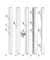
このような作製方法を用いると、半導体活性層表面において、従来の多結晶半導体膜において結晶粒界に沿って形成されるリッジが形成されず、粒界は平坦であるか緩やかな凹部を形成していることが確認された。図1、図2には、本発明、及び従来の半導体記憶素子の典型的な構造(模式図)を示す。
【0017】
図2に示すのは、従来方法として、エキシマレーザーによるレーザー結晶化や、熱結晶化を用いて作製した半導体記憶素子の模式的な構造であり、(1)、(2)はそれぞれ平面図、チャネル方向断面図である。図2において、半導体記憶素子は、絶縁表面を有する基板201上に、チャネル領域202と、一対の一導電型不純物領域203、204からなる半導体活性層、第1ゲート絶縁膜205、浮遊ゲート電極206、第2ゲート絶縁膜207、制御ゲート電極208が積層された構造となっている。
【0018】
図2において、平面図に示すように、半導体膜は点線で表された結晶粒が集合して形成され、結晶粒は特に一方向に延在することなくランダムな形状となっている。また、断面図に示されているように結晶粒の境界(以下、結晶粒界と記す)に沿って表面にリッジが形成され、半導体活性層表面の凸凹は大きくなっている。
【0019】
一方、図1に示すのは、本発明における半導体記憶素子の模式的な構造であり、(1)、(2)はそれぞれ平面図、チャネル方向断面図である。図1において、半導体記憶素子は、絶縁表面を有する基板101上に、チャネル領域102と、一対の一導電型不純物領域103、104からなる半導体活性層、第1ゲート絶縁膜105、浮遊ゲート電極106、第2ゲート絶縁膜107、制御ゲート電極108が積層された構造となっている。
【0020】
図1において、半導体膜を構成する結晶粒は一方向に延在した構造となっている。また、結晶粒界に沿って表面にリッジが形成されることはなく、粒界は平坦であるか緩やかな凹部を形成しており、半導体活性層表面は平坦になっている。
【0021】
なお、結晶粒の延在する方向は、レーザー光を走査する方向と一致する。また、本発明によって作製される半導体活性層を構成する結晶粒の大きさ(以下、グレインサイズとも呼ぶ)は、短手方向に0.5μm〜100μm、長手方向に3μm〜10000μm程度となる。
【0022】
なお、レーザーをチャネル方向に平行に走査した場合は、垂直に走査した場合と比較して、TFT及び半導体記憶素子の駆動能力は向上する。これは、結晶粒界がレーザーの走査方向とおおむね平行に形成されるため、レーザーをチャネル方向と平行に走査することによって、チャネルを横切る結晶粒界の本数を低減できるためである。
【0023】
本発明の半導体記憶装置は、半導体記憶素子を形成する基板上に、半導体記憶素子を選択するデコーダ回路、書き込み・読み出し回路等の周辺回路や、他の半導体集積回路を有していてもよい。その場合、メモリの高速動作を実現するために、半導体記憶素子や周辺回路や他の半導体集積回路を構成するTFTでは、レーザー光をチャネル方向に平行に走査することが好ましい。勿論、本発明では、チャネル領域の活性層表面を平坦にする目的において、レーザーの走査方向はチャネル方向に限定されない。
【0024】
なお、本発明でいう半導体記憶装置とは、EEPROM(Electrically Erasable and Programmable Read Only Memory)やフラッシュメモリといった不揮発性メモリ、および、そのような不揮発性メモリを半導体記憶部として有する半導体装置全般を指す。例えば、不揮発性メモリを半導体記憶部として有するマイクロプロセッサ、半導体表示装置(代表的には液晶表示装置およびEL表示装置)をその範疇に含む。
【0025】
なお、図1及び図2には、一例として、電荷蓄積層からなる浮遊ゲート電極を有する半導体記憶素子の形態を示した。また、不純物領域は、浮遊ゲート電極と重ならない構成を示したが、消去時(或いは書き込み時)に浮遊ゲートから電荷を引き抜く目的で、第1ゲート絶縁膜を介して浮遊ゲート電極と一部重なっていてもよい。
【0026】
次に、具体的なデータとして、多結晶半導体膜表面のAFM像および断面TEM像を図3、4に示す。
【0027】
図3(1)には従来の多結晶半導体膜のAFM像を、また、図3(2)には連続発振レーザーを用いて形成した多結晶半導体膜のAFM像を示す。
【0028】
図3において、画像301及び303は、表面の凹凸をグレースケールで表した、10μm四方の画像である。また、画像302及び304は、平均の高さを境界として、表面の高さを2値で表した画像と、縦方向および横方向の断面での凹凸を表したグラフである。
【0029】
図3(1)に示した半導体膜は、触媒元素としてNiを用い、熱結晶化(450℃、4h)を行った試料である。図3(1)において、多結晶半導体膜は、0.3μm程度の形状異方性を持たない結晶粒が集合してなる様子が確認できる。また、図3(2)に示した半導体膜は、Nd:YVO4レーザーの第2高調波を用い、出力8W、走査速度75cm/sでもって走査することで結晶化を行った試料である。図3(2)において、多結晶半導体膜は、短手方向0.2〜2μm程度、長手方向10μm以上の横方向に延在した結晶粒が集合してなる様子が確認でききる。
【0030】
各AFM像によって表面粗さを評価すると、熱結晶化による試料では、10μm×10μm内のP−V(peak to valley)値で73nm、rms(root mean square)値で10nmであるが、レーザー結晶化を行った試料では、10μm×10μm内のP−V値で38nm、rms値(root mean square)で3.2nmとなっており、レーザー結晶化を行った試料が、熱結晶化を行った試料と比較して、表面が非常に平坦になっていることがわかる。
【0031】
このように、本発明において、半導体活性層の表面は、P−V値で0.1nm〜60nm、好ましくは1〜40nmを実現することができ、rms値(root mean square)で0.1nm〜5nm、好ましくは1〜3.5nmを実現することができる。
【0032】
また、図4(1)には、従来の多結晶半導体膜の断面TEM像を、図4(2)には、連続発振レーザーを用いて形成した多結晶半導体膜の断面TEM像を示す。
【0033】
各TEM像は、ともに20万倍の倍率であり、図4において、薄膜401及び405は下地膜、薄膜402及び406は多結晶半導体膜、薄膜403、407はゲート絶縁膜、黒色の薄膜404、408はゲート電極である。
【0034】
また、図4(1)に示した半導体膜は、触媒元素としてNiを用い、熱結晶化(450℃、4h)を行った試料であり、図3(2)に示した半導体膜は、Nd:YVO4レーザーの第2高調波を用い、出力7W、走査速度50cm/sでもって走査することで結晶化を行った試料である。
【0035】
レーザー結晶化を行った試料は、多結晶半導体膜に黒っぽい模様の見られる数個所においてわずかな歪みが見られるが、全体的にほぼ平坦であることがわかる。一方、熱結晶化を行った試料は全体に模様が入り、半導体膜表面も全体に凹凸が大きく、上層のゲート酸化膜においても凹凸が反映されている様子が見て取れる。
【0036】
このように、本発明では、連続発振レーザーを用い、半導体膜にレーザー光を照射して溶融し、これを連続的に走査して結晶化させることによって、チャネル領域において結晶粒界上のリッジが抑えられ、半導体活性層表面を非常に平坦にすることが可能となる。その結果、活性層表面において極端に電界が集中する領域が低減され、第1ゲート絶縁膜の信頼性を向上することが可能となる。
【0037】
次に、上述した方法によって作製したTFT及び半導体記憶素子を微細化してゆく場合の問題点について述べる。
【0038】
微細化を進める際には、加工精度の改善と、微細素子の特性の問題が挙げられるが、加工精度に関しては、液晶ディスプレイに通常用いられる、凹凸やうねりの大きなガラス基板上であっても、分解能の高い露光装置(i線ステッパなど)を用い、露光時の焦点深度を大きくとることで、サブミクロンまでの加工は可能である。一方、上述したレーザー光の照射による結晶化工程を用いて作製したTFTは、勿論プロセス条件にもよるが、ゲート長がサブミクロンに至る前に特性に問題が現れることがわかった。
【0039】
図5(1)に、上述したレーザーによる結晶化工程を用いて作製したTFTのVG−ID曲線を示す。本試料は、Nd:YVO4レーザーの第2高調波を用い、出力7W、走査速度50cm/sでもって走査することで結晶化を行ったTFTであり、チャネル長L=1.3μm、チャネル幅W=8μm、半導体活性層膜厚54nm、ゲート絶縁膜厚55nmである。また、VD=5Vである。
【0040】
図5(1)に示したTFT特性は、VD=1Vでは正常な振る舞いが見られるが、VD=5Vではオフ電流に明らかな異常が見られる。このことは、電源電圧5Vでは本試料がスイッチング機能をほとんど有さず、半導体記憶素子あるいはTFTとして使用できないことを意味する。
【0041】
本発明はこのような特性異常を抑えるために、レーザー光照射による結晶化工程の前に、金属元素を用いた加熱処理を行うことを特徴とする。図5(2)には、そのような方法によって作製したTFTのVG−ID曲線が示されている。本試料は、レーザー光照射の条件は破線に示した試料と同じであるが、その前に金属触媒としてNiを添加した熱処理工程(450℃、4h)を行っている。チャネル長L=1.3μm、チャネル幅W=8μm、半導体活性層膜厚54nm、ゲート絶縁膜厚55nmである。
【0042】
図5に見られるように、金属元素を用いた加熱処理を行ったTFTは、これを行わない場合と異なり、VD=5Vにおいても、オフ電流の異常はなく、正常な電流特性が確認される。
【0043】
このように、連続発振レーザーを用いた結晶化工程の前に、金属元素を用いた加熱処理を加えることによって、TFTや半導体記憶素子の微細化に伴って生じる特性異常を抑える効果があることが判明した。その結果、本発明では、より微細なTFTや半導体記憶素子を実現することが可能となる。
【0044】
勿論、ここで示したチャネル長L=1.3μmは一例である。金属元素を用いた加熱処理を行ったTFTは、主に、チャネル長2μm以下において、これを行わない場合と比較して、オフ電流の異常を抑える効果が見られた。従って、本発明において、半導体記憶素子及びTFTのチャネル長はL=0.01μm〜2μmとすることで効果がある。
【0045】
また、本発明における半導体記憶素子及びTFTの作製工程では、添加した金属元素を取り除くゲッタリング工程にも依存するが、作製した半導体活性層には、金属元素が1×10¹⁶/cm3〜5×1018/cm3の濃度で含まれる場合がある。
【0046】
本発明の作製方法を用いることで、半導体活性層表面が平坦であり、かつ、微細な半導体記憶素子およびTFTを実現することが可能となる。半導体活性層表面が平坦であることは、半導体記憶素子の書き換え耐性が高いことを意味し、信頼性の高い不揮発性メモリを実現することができる。また同時に微細な半導体記憶素子およびTFTを実現できることで、素子面積を縮小することができ、面積の小さい、あるいは同面積で容量の大きい不揮発性メモリを実現することができる。
【0047】
本発明によって、絶縁表面を有する基板上に形成され、チャネル領域と一導電型不純物領域からなる半導体活性層、第1ゲート絶縁膜、電荷蓄積層、第2ゲート絶縁膜、及び制御ゲート電極を備えた半導体記憶素子であって、以下の(1)、(2)、(3)の特徴を同時に有する半導体記憶素子を実現することができる。
【0048】
(1)前記半導体活性層は金属元素を1×10¹⁶/cm3〜5×1018/cm3の濃度で含む、あるいは、前記半導体活性層は金属を添加した半導体膜の加熱処理を行った多結晶半導体膜である、あるいは、前記半導体記憶素子のチャネル長は0.01μm〜2μmである。
(2)前記チャネル領域は、レーザー光を照射する際に少なくとも同一チャネル領域において連続的に走査することによって結晶化された多結晶半導体膜である、あるいは、前記半導体活性層は同一方向に延在する複数の結晶粒が集合してなる多結晶半導体膜である。
(3)前記半導体活性層を構成する結晶粒の粒界は平坦であるか凹部を形成していること、あるいは、前記チャネル領域の表面粗さがP−V値0.1nm〜60nmである、あるいは、前記チャネル領域の表面粗さがrms値0.1nm〜5nmである
ことを特徴とする半導体記憶素子。
【0049】
なお、前記金属元素は、Fe、Ni、Co、Ge、Sn、Pd、Pt、Cu、Auから選ばれた一種または複数種であることが好ましい。
【0050】
本発明によって、前記半導体記憶素子がマトリクス状に配置されてなるメモリセルアレイを有することを特徴とする半導体記憶装置が提供される。
【0051】
本発明によって、前記半導体記憶素子がマトリクス状に配置されてなるメモリセルアレイが、プラスチック基板上もしくはセラミック基板上に形成されていることを特徴とする半導体記憶装置が提供される。
【0052】
本発明によって、前記半導体記憶素子がマトリクス状に配置されてなるメモリセルアレイを有する不揮発性メモリが積層されてなるICチップを有することを特徴とする半導体記憶装置が提供される。
【0053】
前記半導体記憶装置として、ゲーム機、ビデオカメラ、頭部取り付け型のディスプレイ、DVDプレーヤー、パーソナルコンピュータ、携帯電話、あるいはカーオーディオが提供される。
【0054】
本発明によって、絶縁表面を有する基板上の半導体記憶素子の作製方法であって、前記絶縁表面を有する基板上に非晶質半導体膜を形成し、前記非晶質半導体膜に結晶化を助長する金属元素を添加し、前記非晶質半導体膜を加熱処理し、前記非晶質半導体膜にレーザー光を照射し、少なくとも同一チャネル領域において該レーザー光を連続的に走査することによって、多結晶半導体膜を形成し、前記多結晶半導体膜上に第1ゲート絶縁膜を形成し、前記第1ゲート絶縁膜に積層して電荷蓄積層、第2ゲート絶縁膜、および制御ゲート電極を形成することを特徴とする半導体記憶素子の作製方法が提供される。
【0055】
【発明の実施の形態】
(実施形態1)
本発明における多結晶半導体膜の作製方法の一形態について説明する。説明には、図6を用いる。
【0056】
まず図6(A)に示すように、基板600上に下地膜601を成膜する。基板600には、例えばバリウムホウケイ酸ガラスや、アルミノホウケイ酸ガラスなどのガラス基板、石英基板、SUS基板等を用いることができる。また、プラスチック等の可撓性を有する合成樹脂からなる基板は、一般的に上記基板と比較して耐熱温度が低い傾向にあるが、作製工程における処理温度に耐え得るのであれば用いることが可能である。
【0057】
下地膜601は基板600中に含まれるNaなどのアルカリ金属やアルカリ土類金属が、半導体膜中に拡散し、半導体素子の特性に悪影響を及ぼすのを防ぐために設ける。よってアルカリ金属やアルカリ土類金属の半導体膜への拡散を抑えることができる酸化珪素や、窒化珪素、窒化酸化珪素などの絶縁膜を用いて形成する。本実施の形態では、プラズマCVD法を用いて窒化酸化珪素膜を10〜400nm(好ましくは50〜300nm)の膜厚になるように成膜した。
【0058】
なお下地膜601は単層であっても複数の絶縁膜を積層したものであっても良い。また、石英基板など不純物の拡散がさして問題とならない場合は、必ずしも設ける必要はない。
【0059】
次に下地膜上に半導体膜602を形成する。半導体膜602の膜厚は25〜100nm(好ましくは30〜60nm)とする。なお半導体膜602は、非晶質半導体であっても良いし、多結晶半導体であっても良い。また半導体は珪素だけではなくシリコンゲルマニウムも用いることができる。シリコンゲルマニウムを用いる場合、ゲルマニウムの濃度は0.01〜4.5atomic%程度であることが好ましい。
【0060】
次に図6(B)に示すように、半導体膜602の表面に、重量換算で1〜100ppmのNiを含む酢酸ニッケル塩溶液をスピンコート法で塗布した。なお触媒の添加は上記方法に限定されず、スパッタ法、蒸着法、プラズマ処理などを用いて添加しても良い。
【0061】
次に、500〜650℃で4〜24時間、例えば570℃、14時間の加熱処理を行った。この加熱処理により、酢酸ニッケル塩溶液が塗布された表面から、基板600に向かって縦方向に結晶化が促進された半導体膜603が形成される(図6(B))。
【0062】
なお、本実施の形態では触媒元素としてニッケル(Ni)を用いているが、その以外にも、ゲルマニウム(Ge)、鉄(Fe)、パラジウム(Pd)、スズ(Sn)、鉛(Pb)、コバルト(Co)、白金(Pt)、銅(Cu)、金(Au)といった元素を用いても良い。
【0063】
次に図6(C)に示すように、半導体膜603にレーザー光を照射して結晶化する。多結晶半導体膜を溶融して、これを連続的に走査して結晶化させる手段としては、気体レーザー発振装置、固体レーザー発振装置を光源とする連続発振レーザー光を適用する。照射するレーザー光は光学系にて線状に集光されたものであり、その強度分布が長手方向において均一な領域を有し、短手方向に分布を持っていても良く、光源として用いるレーザー発振装置は、矩形ビーム固体レーザー発振装置が適用され、特に好ましくは、スラブレーザー発振装置が適用される。
【0064】
線状に集光され長手方向に拡張されたレーザー光を非晶質半導体膜あるいは多結晶半導体膜に照射し、且つレーザー光の照射位置と半導体膜が形成された基板とを相対的に動かして、レーザー光が一部又は全面を走査することにより半導体膜を溶融させ、その状態を経て結晶化又は再結晶化を行う。
【0065】
連続発振が可能な固体レーザーを用い、基本波の第2高調波〜第4高調波を用いることで、大粒径の結晶を得ることができる。例えば、代表的には、Nd:YVO4レーザー(基本波1064nm)の第2高調波(532nm)や第3高調波(355nm)を用いるのが望ましい。具体的には、連続発振のYVO4レーザーから射出されたレーザー光を非線形光学素子により高調波に変換し、出力10Wのレーザー光を得る。また、共振器の中にYVO4結晶と非線形光学素子を入れて、高調波を射出する方法もある。そして、好ましくは光学系により照射面にて矩形状または楕円形状のレーザー光に成形して、半導体膜603に照射する。このときのエネルギー密度は0.01〜100MW/cm2程度(好ましくは0.1〜10MW/cm2)が必要である。そして、10〜2000cm/s程度の速度でレーザー光に対して相対的に非晶質半導体膜604を移動させて照射する。
【0066】
なお、本発明によって得られる結晶粒は、レーザー光の走査方向に延在した形状を有し、結晶粒径は、短手方向で、0.5μm〜100μm、長手方向で、1μm〜10000μm程度となる。
【0067】
上述した半導体膜603へのレーザー光の照射により、結晶性がより高められた半導体膜605が形成される。
【0068】
なお、金属元素を用いて加熱処理を行った半導体膜605内には、金属元素(ここではNi)がおおよそ1×10¹⁹atoms/cm3程度の濃度で含まれていると考えられる。次に、半導体膜605内に存在する金属元素のゲッタリングを行う。
【0069】
まず、図6(D)に示すように半導体膜605の表面に酸化膜606を形成する。1〜10nm程度の膜厚を有する酸化膜606を形成することで、後のエッチング工程において半導体膜605の表面がエッチングにより荒れるのを防ぐことができる。
【0070】
酸化膜606は公知の方法を用いて形成することができる。例えば、硫酸、塩酸、硝酸などと過酸化水素水を混合させた水溶液や、オゾン水で、半導体膜605の表面を酸化することで形成しても良いし、酸素を含む雰囲気中でのプラズマ処理や、加熱処理、紫外線照射等により形成しても良い。また酸化膜を別途、プラズマCVD法やスパッタ法、蒸着法などで形成しても良い。
【0071】
次に酸化膜606上に、希ガス元素を1×10²⁰ atoms/cm3以上の濃度で含むゲッタリング用の半導体膜607を、スパッタ法を用いて25〜250nmの厚さで形成する。ゲッタリング用の半導体膜607は、半導体膜605とエッチングの選択比を大きくするため、半導体膜605よりも膜の密度の低い方がより望ましい。
【0072】
希ガス元素としてはヘリウム(He)、ネオン(Ne)、アルゴン(Ar)、クリプトン(Kr)、キセノン(Xe)から選ばれた一種または複数種を用いる。
【0073】
次にファーネスアニール法やRTA法を用いて加熱処理を施し、ゲッタリングを行う。ファーネスアニール法で行う場合には、窒素雰囲気中にて450〜600℃で0.5〜12時間の加熱処理を行う。また、RTA法を用いる場合には、加熱用のランプ光源を1〜60秒、好ましくは30〜60秒点灯させ、それを1〜10回、好ましくは2〜6回繰り返す。ランプ光源の発光強度は任意なものとするが、半導体膜が瞬間的には600〜1000℃、好ましくは700〜750℃程度にまで加熱されるようにする。
【0074】
加熱処理により、半導体膜605内の触媒元素が、拡散により矢印に示すようにゲッタリング用の半導体膜607に移動し、ゲッタリングされる。
【0075】
次にゲッタリング用の半導体膜607をエッチングして除去する。エッチングは、ClF3によるプラズマを用いないドライエッチング、或いはヒドラジンや、テトラエチルアンモニウムハイドロオキサイド((CH3)4NOH)を含む水溶液などアルカリ溶液によるウエットエッチングで行うことができる。この時酸化膜606によって半導体膜605がエッチングされるのを防ぐことができる。
【0076】
次に酸化膜606を、フッ酸により除去する。
【0077】
なお、本発明においてゲッタリング工程は、本実施の形態に示した方法に限定されない。その他の方法を用いて半導体膜中の金属元素を低減するようにしても良い。
【0078】
次に、図6(E)に示すように半導体膜603をパターニングし、島状の半導体膜608〜610が形成され、該島状の半導体膜608〜610を用いて半導体記憶素子やTFTが形成される。
【0079】
なお、本実施形態のように、レーザー光の照射による結晶化を行うことで、表面が非常に平坦な半導体膜を作製することができる。また、金属元素の添加と熱処理工程によって、これを行わない場合と比較してより微細なTFTを作製することができる。
【0080】
そして、上記のように作製した半導体膜を、半導体記憶素子およびTFTの活性層として用いることにより、信頼性が高く、小型の不揮発性メモリを有する半導体記憶装置を実現することができる。
【0081】
(実施形態2)
次に、実施形態1で説明した作製方法に従って形成した島状半導体膜を用いて、不揮発性メモリを作製する一形態について説明する。説明には図7を用いる。
【0082】
本実施形態では、メモリセルと周辺回路を同時に作製する形態を示し、図面の右側には半導体記憶素子の作製工程を、左側には、周辺回路を代表するnチャネル型TFTとpチャネル型TFTの作製工程を示す。
なお、TFTはシングルドレイン構造とし、半導体記憶素子には消去時に電荷を引き抜くためのオーバーラップ領域を設ける構造とする。
【0083】
図7(A)に示す島状半導体膜701〜703は、実施形態1に従って作製する。このとき、表面粗さの観点からは、レーザー光の走査方向は任意で構わないが、半導体記憶素子やTFTの駆動能力を向上する目的において、レーザー光の走査方向をチャネル方向と平行にすることが好ましい。また、互いのばらつきを抑えたい素子間において、チャネル方向とレーザー光の走査方向のなす角を同一にしておくことが好ましい。
【0084】
まず、第1ゲート絶縁膜704としてプラズマCVD法またはスパッタ法を用い、10〜200nmの酸化珪素膜又は酸窒化珪素膜を形成する。
【0085】
なお、絶縁表面を有する基板として石英基板を用いる場合には、半導体記憶素子の第1ゲート絶縁膜を、熱酸化工程により形成してもよい。例えば、酸化雰囲気中で950℃の加熱処理を加え、10〜200nmの熱酸化膜を形成する。これにより、良質な酸化膜と界面準位の少ない半導体/絶縁膜界面が得られ、第1ゲート絶縁膜の高い信頼性が得られる。また、第1ゲート絶縁膜は、酸化珪素膜又は酸窒化珪素膜を形成した後、熱酸化工程を行い、堆積膜と熱酸化膜の積層構造としてもよい。
【0086】
次に、レジストマスク(図示せず)を形成し、n型を付与する不純物元素を選択的に添加し、半導体記憶素子のオーバーラップ領域として機能するn型不純物領域705を形成する。ドーピングは、代表的な方法としてフォスフィン(PH3)を用いたイオンドープ法で行う。n型不純物元素としては、リン(P)の他に砒素(As)を用いてもよい。
【0087】
次に、図7(B)に示すように、第1ゲート絶縁膜704上にゲート電極711、712および浮遊ゲート電極713を形成する。ゲート電極711、712および浮遊ゲート電極713はタンタル(Ta)、チタン(Ti)、モリブデン(Mo)、タングステン(W)、前記元素を主成分とする合金、あるいは多結晶シリコンなどで形成すれば良い。
【0088】
その後、ゲート電極711、712および浮遊ゲート電極713をマスクとして自己整合的にn型不純物元素及びp型不純物元素をそれぞれ添加し、nチャネル型TFTのソース領域またはドレイン領域として機能する高濃度n型不純物領域714〜717、及びpチャネル型TFTのソース領域またはドレイン領域として機能する高濃度p型不純物領域718,719を形成する。n型を付与する不純物元素にはリン(P)あるいは砒素(As)を、p型を付与する不純物元素にはボロン(B)を、それぞれ用いる。
【0089】
次に、図7(C)に示すように、第2ゲート絶縁膜721として、プラズマCVD法またはスパッタ法を用い、10〜200nmの酸化珪素膜又は酸窒化珪素膜を形成する。なお、第2のゲート絶縁膜721として、SiO2/SiN/SiO2による積層膜(ONO膜と呼ばれる)を用いても良い。
【0090】
その後、n型またはp型不純物元素の活性化を行う。活性化手段としては、ファーネスアニール、レーザーアニール、ランプアニール、またはこれらを組み合わせた方法を用いるとよい。熱アニール法では酸素濃度が1ppm以下、好ましくは0.1ppm以下の窒素雰囲気中で400〜700℃で行う。
【0091】
次に、200〜400nmの導電膜を形成し、パターニングを行い制御ゲート電極722を形成する。制御ゲート電極722はタンタル(Ta)、チタン(Ti)、モリブデン(Mo)、タングステン(W)、前記元素を主成分とする合金、あるいは多結晶シリコンなどで形成すれば良い。
【0092】
その後、図7(D)に示すように、制御ゲート電極722および第2ゲート絶縁膜721上に、窒化珪素膜又は酸窒化珪素膜による層間絶縁膜723を形成し、層間絶縁膜723にコンタクトホールを形成し、ソースまたはドレイン配線724〜728を形成する。その後、400〜450℃に熱処理をすることにより窒化珪素膜又は酸窒化珪素膜が含有する水素が放出され島状の半導体膜に対する水素化を行うことができる。
【0093】
こうして、図7(D)に示すように、半導体記憶素子と、nチャネル型TFT及びpチャネル型TFTからなる周辺回路と、を同時に形成することができる。本作製工程により、NOR型、NAND型といった公知のメモリセルアレイや、CMOS回路あるいは単極性TFTからなる周辺回路を作製することができる。
【0094】
また、本実施形態により、周辺回路だけではなく、nチャネル型TFT及びpチャネル型TFTからなるあらゆる回路を作製することが可能となる。特に、CPUや様々なコントローラを同時に形成することも可能であるし、液晶表示装置あるいは発光装置の画素や駆動回路を同時に形成することも可能となる。
【0095】
なお、本実施形態では、シングルドレイン構造を作製する場合について説明したが、フォトレジストをマスクとする方法などの公知の方法を用いて、適宜、低濃度ドレイン領域を設けてもよい。
【0096】
このようして、活性層表面が平坦で、かつ、微細な半導体記憶素子およびTFTを絶縁表面を有する基板上に同時に作製することが可能となる。その結果、信頼性が高く小型で、かつメモリセルアレイ及び周辺回路が同一基板上に形成された不揮発性メモリを有する半導体記憶装置を実現することが可能となる。
【0097】
(実施例1)
本発明の半導体記憶装置の実施例として、不揮発性メモリの回路構成と動作方法について説明する。
【0098】
本発明は、半導体記憶素子の構造や半導体活性層、及びその作製方法に特徴があり、メモリセルの回路構成や動作方法には公知の技術を用いることができる。本実施の形態では、NOR型フラッシュメモリの典型的な回路構成と動作方法について簡単に説明する。
【0099】
図8に、m×nビットの記憶容量を有するNOR型フラッシュメモリのブロック回路図を示す。図8に示したNOR型フラッシュメモリは、複数のメモリセル(1、1)〜(n、m)が縦m個×横n個のマトリクス状に配置されたメモリセルアレイ801と、Xアドレスデコーダ803、Yアドレスデコーダ802、Yセレクタ804、書き込み・読み出し回路805といった周辺回路によって構成されている。他の周辺回路として、昇圧回路、アドレスバッファ回路等が設けられてもよい。
【0100】
各メモリセル(代表として、メモリセル(i、j)を考える。ここで、iは1以上n以下の整数、jは1以上m以下の整数)は、nチャネル型の半導体記憶素子によって構成される。そして、半導体記憶素子のドレイン電極と制御ゲート電極は、ビット線BL(i)とワード線WL(j)にそれぞれ接続されている。また、ビット線BL(1)〜BL(n)はYアドレスデコーダ802に、ワード線WL(1)〜WL(m)はXアドレスデコーダ803にそれぞれ接続されている。また、全ての半導体記憶素子のソース電極は共通のソース線に接続されており、ソース線電位Vsが与えられている。
【0101】
データの書き込みと読み出しは、Xアドレスデコーダ803およびYアドレスデコーダ802によって選択されたメモリセルにおいて行われる。メモリセル(1、1)を例にとって、ホットエレクトロンによる書き込み動作、読み出し動作ついて説明する。
【0102】
まず、半導体記憶素子にデータを書き込む場合は、ソース線をGNDに落し、ビット線BL(1)およびワード線WL(1)に、それぞれ正の高電圧(例えば16V)を印加する。このような条件下では、半導体記憶素子のドレイン近傍での高電界により、インパクトイオン化が起こる。さらにゲート方向にも高電界が生じるために、発生したホットエレクトロンは浮遊ゲート電極に注入され、書き込みが行われる。半導体記憶素子のしきい値電圧は、浮遊ゲート電極に蓄積された電荷量に応じて変化する。
【0103】
半導体記憶素子に格納されたデータを読み出す場合は、ソース線をGNDに落し、ワード線WL(1)に所定の電圧を印加する。所定の電圧は、書き込み後のしきい値電圧と消去後のしきい値電圧との間に設定すればよい。その結果、消去後の半導体記憶素子のみがオン状態となることを利用して、メモリセル(1、1)に記憶されているデータをビット線BL(1)から読み出す。
【0104】
例えば、半導体記憶素子の2状態のしきい値電圧がそれぞれ2V以下、および4V以上である場合には、所定の電圧として3Vを用いることができる。
【0105】
データの消去は、選択された複数のメモリセルに対して同時に行われる。例えば、第1列目のメモリセル(1,1)〜(m,1)を消去する場合、ソース線およびワード線W1をGNDに落し、ビット線B1に正の高電圧(例えば20V)を印加する。この時、半導体記憶素子のゲート・ドレイン間に高い電位差が生じるため、浮遊ゲート電極に蓄積されている電子がトンネル電流によってドレイン領域へ放出され、消去が行われる。このように、半導体記憶素子のドレイン領域から電荷を引き抜く場合には、ドレイン側の高濃度不純物領域と浮遊ゲート電極とが第1ゲート絶縁膜を介して一部重なっていることが好ましい。
【0106】
なお、書き込み、読み出しおよび消去時において選択されていない信号線BL(2)〜BL(n)、WL(2)〜WL(m)の電位は全て0Vとすればよい。また、上述した動作電圧の値は一例であって、その値に限られるわけではない。
【0107】
なお、本実施例では、1つの半導体記憶素子に2値(1ビット)の情報を格納する場合を説明したが、しきい値電圧の制御をより正確に行うことによって、1つの半導体記憶素子に3値以上の情報を格納する多値の不揮発性メモリとすることも可能である。また、1つの半導体記憶素子と1つの選択用のTFTでもってメモリセルを構成するタイプの不揮発性メモリであってもよいし、選択用のTFTと半導体記憶素子との役割を合わせ持つスプリットゲート構造の半導体記憶素子でもってメモリセルを構成するタイプの不揮発性メモリであっても構わない。
【0108】
(実施例2)
本実施例では、実施例1に示した不揮発性メモリの回路構成とは異なる例として、NAND型フラッシュメモリの説明を行う。
【0109】
図9は、nチャネル型半導体記憶素子が縦8個×横n個のマトリクス状に配列されたNAND型のメモリセルアレイの回路図である(両端の列のみ図示)。
【0110】
図8において、同じ列に配置された8つの半導体記憶素子(i、1)〜(i、8)(i=1〜n)は直列に接続されると共に、チャネル形成領域が配線Giに接続されている。配線G1〜Gnは共通配線となっており、電位Vbが与えられる。また、同じ行に配置されたn個の半導体記憶素子(1、j)〜(n、j)(j=1〜8)は、制御ゲート電極がワード線Wjに接続されている。
【0111】
直列に接続された8つの半導体記憶素子(i、1)〜(i、8)(i=1〜n)の両端には、選択用TFT(i、0)及び(i、9)が直列に接続されている。そして、選択用TFT(i、0)のソース電極及びドレイン電極の残る一方にはビット線Biが接続されており、ゲート電極には選択用ゲート線S1が接続されている。また、選択用TFT(i、9)のソース電極及びドレイン電極の残る一方には共通のソース電位Vsが与えられており、ゲート電極には選択用ゲート線S2が接続されている。
【0112】
NAND型フラッシュメモリの動作方法について述べる。ここでは、トンネル電流による一括消去と、トンネル電流による一行同時書き込みの方法について説明する。
【0113】
本実施例において、"0"の状態とは半導体記憶素子の浮遊ゲート電極に電荷を注入した状態を指し、"1"の状態とは半導体記憶素子の浮遊ゲート電極から電荷が放出された状態を指す。また、"0"の状態の半導体記憶素子のしきい値電圧は0.5V〜3Vであるとし、"1"の状態の半導体記憶素子のしきい値電圧は−1V以下であるとする。
【0114】
まず、一行同時書き込みについて述べる。具体例として、一行目の同時書き込みを考え、半導体記憶素子(1、1)に"0"を、半導体記憶素子(2、1)〜(n、1)に"1"を書き込む場合を説明する。なお、書き込む直前は全て"1"の状態とする。まず、電位Vbとソース電位VsをGNDに落す。また、選択用ゲート線S1、S2にそれぞれ20V、0Vを印加し、選択用TFT(1、0)〜(n、0)をオンの状態に、選択用TFT(1、9)〜(n、9)をオフの状態にする。そしてワード線W1に20V、ワード線W2〜W8に7Vを印加すると共に、ビット線B1に0V、ビット線B2〜Bnに7Vを印加する。
【0115】
その結果、半導体記憶素子(1、1)の浮遊ゲート電極−チャネル形成領域間にのみ高電圧(約20V)が印加され、トンネル電流による浮遊ゲート電極への電荷注入が行われる。つまり、"0"が書き込まれる。また、半導体記憶素子(2、1)〜(n、1)の浮遊ゲート電極−チャネル形成領域間には14V程度の電位差が生じるのみであり、トンネル電流による浮遊ゲート電極への電荷注入は行われない。つまり、半導体記憶素子(2、1)〜(n、1)は"1"の状態のままとなる。また、一行目以外の半導体記憶素子についても、浮遊ゲート電極−チャネル形成領域間に高々7Vの電位差が生じるだけであり、浮遊ゲート電極への電荷注入は行われない。このようにして、一行同時書き込みが行われる。
【0116】
半導体記憶素子(1、1)からの読み出しを行う場合は、まず、電位VbをGNDに落し、ワード線W1に0V、ワード線W2〜W8に5Vを印加する。これにより、2行目から8行目の半導体記憶素子は全てオンの状態となる。また、1行目の半導体記憶素子は、"1"の状態であればオンの状態となり、"0"の状態であればオフの状態となる。つまり、直列に接続された8つの半導体記憶素子の導通、非導通は、1行目の半導体記憶素子の状態で決まることになる。そして、選択用ゲート線S1、S2に5Vを印加し選択用TFTをオンの状態とすると共に、ソース電位VsをGNDに落すことにより、ビット線B1を通して、半導体記憶素子(1、1)からのデータの読み出しを行うことが可能となる。
【0117】
一括消去を行う場合は、全てのワード線W1〜W8を0Vとし、電位Vbを20Vとする。その結果、浮遊ゲート電極−チャネル形成領域間に高電圧が印加され、トンネル電流による消去が行われる。なお、選択用ゲート線の電位は自由に決めて良いが、ゲート酸化膜に強い電界が生じないように、電位Vbと同程度の電圧を印加することが好ましい。
【0118】
なお、上述した動作電圧の値は、一例であって、その値に限られるわけではない。また、本実施例では、縦8個×横n個のメモリセルアレイについて説明したが、この構成に限定する必要はない。
【0119】
本発明は、このようなNAND型フラッシュメモリに対しても適用することができ、信頼性が高く、小型のメモリを実現することができる。
【0120】
(実施例3)
本実施例では、結晶化に際し適用することのできるレーザー処理装置の構成の一例を示す。
【0121】
図10はレーザー発振装置1001a、1001b、シャッター1002、高変換ミラー1003〜1006、シリンドリカルレンズ1008、1009、スリット1007、載置台1011、載置台1011をX方向及びY方向に変位させる駆動手段1012、1013、当該駆動手段をコントロールする制御手段1014、予め記憶されたプログラムに基づいてレーザー発振装置1001や制御手段1014に信号を送る情報処理手段1015などから成っているレーザー処理装置の構成を正面図と側面図により示すものである。
【0122】
レーザー発振装置は矩形ビーム固体レーザー発振装置が適用され、特に好ましくは、スラブレーザー発振装置が適用される。或いは、YAG、YVO4、YLF、YAlO3などの結晶にNd、Tm、Hoをドープした結晶を使った固体レーザー発振装置にスラブ構造増幅器を組み合わせたものでも良い。スラブ材料としては、Nd:YAG、Nd:GGG(ガドリニウム・ガリウム・ガーネット)、Nd:GsGG(ガドリニウム・スカンジウム・ガリウム・ガーネット)などの結晶が使用される。その他にも、連続発振可能な気体レーザー発振装置、固体レーザー発振装置を適用することもできる。連続発振固体レーザー発振装置としてはYAG、YVO4、YLF、YAlO3などの結晶にCr、Nd、Er、Ho、Ce、Co、Ti又はTmをドープした結晶を使ったレーザー発振装置を適用する。発振波長の基本波はドープする材料によっても異なるが、1μmから2μmの波長で発振する。5W以上のより高い出力を得る為には、ダイオード励起の固体レーザー発振装置をカスケード接続しても良い。
【0123】
このようなレーザー発振装置から出力される円形状又は矩形状のレーザー光は、シリンドリカルレンズ1008、1009により照射面の断面形状において線状に集光される。また、照射面での干渉を防ぐため、高変換ミラーを適宜調節して10〜80度の角度を持って斜め方向から入射する構成となっている。シリンドリカルレンズ1008、1009は合成石英製とすれば高い透過率が得られ、レンズの表面に施されるコーティングは、レーザー光の波長に対する透過率が99%以上を実現するために適用される。勿論、照射面の断面形状は線状に限定されず、矩形状、楕円形又は長円形など任意な形状としても構わない。
【0124】
また、連続発振レーザー光の波長は、半導体膜の光吸収係数を考慮して400〜700nmであることが望ましい。このような波長帯の光は、波長変換素子1010を用いて基本波の第2高調波〜4高調波を取り出すことで得られる。波長変換素子としてはADP(リン酸二水素化アンモニウム)、Ba2NaNb5O15(ニオブ酸バリウムナトリウム)、CdSe(セレンカドミウム)、KDP(リン酸二水素カリウム)、LiNbO3(ニオブ酸リチウム)、Se、Te、LBO、BBO、KB5などが適用される。特にLBOを用いることが望ましい。
【0125】
また、載置台1011を駆動手段1012、1013により二軸方向に動かすことにより基板1020のレーザー処理を可能としている。一方の方向への移動は基板1020の一辺の長さよりも長い距離を1〜200cm/sec、好ましくは5〜50cm/secの等速度で連続的に移動させることが可能であり、他方へは線状ビームの長手方向と同程度の距離を不連続にステップ移動させることが可能となっている。レーザー発振装置1001a、1001bの発振と、載置台1011は、マイクロプロセッサを搭載した情報処理手段1015により同期して作動するようになっている。
【0126】
載置台1011は図中で示すX方向に直線運動をすることにより、固定された光学系から照射されるレーザー光で基板全面の処理を可能としている。位置検出手段1016は基板1020がレーザー光の照射位置にあることを検出して、その信号を情報処理手段1015に伝送し、情報処理手段1015によりレーザー発振装置1001a、1001bの発振動作とのタイミングを同期させている。つまり、基板1020がレーザー光の照射位置にない時は、レーザーの発振を止めその寿命を延長させている。
【0127】
このような構成のレーザー照射装置により基板1020に照射されるレーザー光は、図中に示すX方向又はY方向に相対移動させることにより半導体膜の所望の領域または全面を処理することができる。
【0128】
なお、本実施例は、実施例1、2のいずれの構成とも自由に組み合わせることが可能である。
【0129】
(実施例4)
本実施例では、連続発振のレーザー光により結晶化した多結晶半導体膜を用いて、半導体記憶素子およびTFTを形成し、転写を行うことでICチップを作製する形態、あるいはプラスチック基板上に転写する形態について説明する。
【0130】
まず、スパッタ法を用いて、絶縁表面を有する第1の基板上に金属膜を成膜する。ここでは金属膜にタングステンを用い、膜厚を10nm〜200nm、好ましくは50nm〜75nmとする。なお本実施例では第1の基板上に直接金属膜を成膜するが、例えば酸化珪素、窒化珪素、窒化酸化珪素等の絶縁膜で第1の基板を覆ってから、金属膜を成膜するようにしても良い。
【0131】
そして金属膜の成膜後、金属表面を酸化して金属酸化膜を形成し、さらに酸化膜を成膜する。本実施例では、金属酸化膜として酸化タングステンをプレスパッタ法により数nm形成し、酸化膜として酸化珪素膜を膜厚150nm〜300nmとなるように成膜する。一連の工程は、スパッタ装置を用いて大気に曝すことなく行った。
【0132】
次にプラズマCVD法を用いて下地膜を成膜する。本工程より先は、実施形態1に説明した作製方法によって、表面が平坦な島状の多結晶半導体膜を形成することができる。
【0133】
さらに、実施形態2に説明した作製方法に従って、半導体記憶素子及びTFTを図14(A)に示すように作製することができる。
【0134】
図14(A)には、絶縁表面を有する基板1401上に、金属膜1402、金属酸化膜1403、酸化膜1404、下地膜1405が積層され、その上に半導体記憶素子及びTFT、及び配線1407〜1411が形成されている。なおTFTの作製方法は、実施形態2に示した工程に限定されない。
【0135】
次に、図14(B)に示すように、第2の層間絶縁膜1412を成膜した後、コンタクトホールを形成し、該コンタクトホールを介して配線1407と接続するパッド1413を形成する。なお、パッド1413とTFTとの電気的な接続の形態は、本実施例に限定されない。
【0136】
次に、第2の層間絶縁膜1412及びパッド1413上に保護層1414を形成する。保護層1414は、後に第2の基板を張り合わせたり剥離したりする際に、第2の層間絶縁膜1412及びパッド1413の表面を保護することができ、なおかつ第2の基板の剥離後に除去することが可能な材料を用いる。例えば、水またはアルコール類に可溶なエポキシ系、アクリレート系、シリコーン系の樹脂を全面に塗布し、焼成することで保護層1414を形成することができる。
【0137】
次に、後の剥離を行い易くするために、金属酸化膜1403を結晶化させる。結晶化により、金属酸化膜1403が結晶粒界において割れやすくなり、脆性を高めることができる。本実施の形態では、400℃〜550℃、0.5〜5時間程度加熱処理を行い、結晶化を行った。
【0138】
次に、金属酸化膜1403と酸化膜1404の間の密着性、または金属酸化膜1403と金属膜1402の間の密着性を部分的に低下させ、剥離開始のきっかけとなる部分を形成する処理を行う。具体的には、剥離しようとする領域の周縁に沿って金属酸化膜1403にレーザー光を部分的に照射したり、或いは、剥離しようとする領域の周縁に沿って外部から局所的に圧力を加えて金属酸化膜1403の層内または界面近傍の一部に損傷を与えたりする。例えば、スクライバー装置を用い、押し込み量を0.1mm〜2mmとし、圧力をかけて動かせばよい。
【0139】
次いで、図14(C)に示すように、両面テープ1416を用い、保護層1414に第2の基板1415を貼り付け、さらに両面テープ1417を用い、第1の基板1401に第3の基板1418を貼り付ける。第3の基板1418は、後の剥離工程で第1の基板1401が破損することを防ぐ。第2の基板1415および第3の基板1418としては、第1の基板1401よりも剛性の高い基板、例えば石英基板、半導体基板を用いることが好ましい。
【0140】
次いで、金属膜1402と酸化膜1404とを物理的に引き剥がす。引き剥がしは、先の工程において、金属酸化膜1403の金属膜1402または酸化膜1404に対する密着性が部分的に低下した領域から開始する。そして第2の基板1415側に半導体素子が、第3の基板1418側に第1の基板1401及び金属膜1402が、それぞれ張り付いたまま分離する。引き剥がしは比較的小さな力(例えば、人間の手、ノズルから吹付けられるガスの風圧、超音波等)で行うことができる。なお、金属酸化膜1403と酸化膜1404は、第2の基板1415側もしくは第3の基板1418側に付着する。
【0141】
このように準備された半導体記憶素子およびTFTは、さまざまな基板に貼り付けて、第2の基板1415を取り除くことで、半導体素子の転写を行うことが可能となる。
【0142】
例えばICチップを作製する場合には、図15(A)に示すように、接着剤1502でインターポーザ(プリント配線基板)1501と、半導体記憶素子およびTFTが貼り付いた第2の基板1415とを接着し、保護層1414から両面テープ1416と第2の基板1415を順に、または同時に剥がす。
【0143】
そして図15(B)に示すように保護層1414を除去し、ワイヤボンディング法を用いて、パッド1413と端子1503をワイヤ1504で接続し、パッケージが完成する。なお、保護層1414は、水溶性の樹脂が使われているので、水に溶かして除去することができる。また、必要に応じて電極表面を洗浄処理やO2プラズマ処理を追加してもよい。
【0144】
インターポーザ1501としては、セラミックス基板、ガラスエポキシ基板、ポリイミド基板等の公知の材料を用いることができる。また、接着剤1502としては、反応硬化型接着剤、熱硬化型接着剤、紫外線硬化型接着剤等の光硬化型接着剤、嫌気型接着剤などの各種硬化型接着剤が挙げられる。
【0145】
なお、本実施例ではソルダーボール1505が設けられたボールグリッドアレイ型のインターポーザを用いるが、本発明はこれに限定されない。端子が周辺に配置されているリードフレーム型のインターポーザであっても良い。
【0146】
本実施例では、CSP(Chip Sized Package)によるパッケージの例を説明したが、この形態に限られない。さらに別のチップを積層したり、並列に配置することも可能であり、MCP(Multi chip Package)によるパッケージを行うこともできる。
【0147】
同様にして、プラスチック基板への転写を行うこともできる。
【0148】
まず、プラスチック基板と、半導体記憶素子およびTFTが貼り付いた第2の基板1415とを接着剤で接着し、保護層1414から両面テープ1416と第2の基板1415を順に、または同時に剥がす。そして保護層1414を除去して、プラスチック基板上への転写が完成する。
【0149】
プラスチック基板としては、2〜30W/mKの高い熱伝導性を有するプラスチック基板を用いることが好ましい。ポリプロピレン、ポリプロピレンサルファイド、ポリカーボネート、ポリエーテルイミド、ポリフェニレンサルファイド、ポリフェニレンオキサイド、ポリサルフォン、またはポリフタールアミドからなる合成樹脂にセラミックスと鉛フリーハンダを混合させ、セラミックスの粒子間をネットワークのようにつながれたプラスチック基板を用いる事が好ましい。
【0150】
以上のようにして、連続発振のレーザー光により結晶化された多結晶半導体膜を用いて、半導体記憶素子およびTFTを形成し、転写を行うことでICチップを作製したり、プラスチック基板上に転写することができる。
【0151】
ICチップとしては、特にMCPによる積層型とすることで、複数の不揮発性メモリチップを積層する場合には小型大容量の不揮発性メモリチップを、不揮発性メモリチップと他のICチップを積層する場合には小型で多機能の不揮発性メモリチップを、それぞれ作製することができる。また、プラスチック基板上に形成することで、半導体基板やガラス基板と比較して頑丈であり、かつ軽量という利点がある。さらに放熱性のよい基板であれば、回路の発熱に対しても優れた形態であり好ましい。
【0152】
なお、本実施例は、実施例1〜3のいずれの構成とも自由に組み合わせることが可能である。
【0153】
(実施例5)
本発明の半導体記憶装置の例として、不揮発性メモリをワンチップ上に集積化されたRISCプロセッサ、ASICプロセッサ等のマイクロプロセッサに適用した場合について説明する。
【0154】
図11に示すのは、マイクロプロセッサの一例である。マイクロプロセッサは典型的にはCPUコア1101、フラッシュメモリ1104、クロックコントローラ1103、キャッシュメモリ1102、キャッシュコントローラ1105、割り込みコントローラ1106、I/Oポート1107等から構成される。もちろん、図11に示すマイクロプロセッサは簡略化した一例であり、実際のマイクロプロセッサはその用途によって多種多様な回路設計が行われる。
【0155】
図11に示すマイクロプロセッサは、実施形態に示した作製方法によって作製することができる。フラッシュメモリ1104のメモリセルには本発明の半導体記憶素子が用いられており、周辺回路、及びCPUコア1101を始めとする各ブロックは、半導体記憶素子と同時に形成されるnチャネル型TFTとpチャネル型TFTによって構成されている。キャッシュメモリとしては、例えばSRAMが用いられている。
【0156】
このように本発明をマイクロプロセッサに応用することにより、信頼性が高く、小面積(あるいは大容量)の不揮発性メモリを有する半導体記憶装置を実現することができる。
【0157】
なお、本実施例は、実施の形態及び実施例1〜4のいずれの構成とも組み合わせることが可能である。
【0158】
(実施例6)
本実施例では、絶縁表面を有する基板上に画像表示部(代表的には、液晶表示部あるいはEL表示部)、不揮発性メモリ、および他の半導体集積回路とを一体形成したシステムオンパネルの形態をとる半導体記憶装置の一例を、図12を用いて説明する。
【0159】
図12において、半導体記憶装置は、画素領域1200、走査線駆動回路1201、信号線駆動回路1202、VRAM1203、フラッシュメモリ1204、CPU1205、画像処理回路1206、ワークメモリ1207及びインターフェース回路1208が、絶縁表面を有する基板1210上に一体形成されてなる。
【0160】
図12に示した半導体記憶装置は、画像データを取り込み、または作製して、画像データの加工とフォーマット変換を行い、画像を表示する装置である。半導体記憶装置としては、例えば、ビデオカメラ、カーナビゲーション、PDA、ゲーム機等を考えることができる。
【0161】
半導体記憶装置は、それぞれの形態に応じて、入力端子から画像データの基となるデータを受信する。例えば、直接外部端子から信号を入力しても良いし、DVテープやメモリーカードとのインターフェースからの入力データであってもよい。入力端子からは、この他、キーボードからの入力信号や他の制御信号が入力される。入力された画像の基となるデータは、システムバスを介して、フラッシュメモリ1204格納にされたり、ワークメモリ1207に一時的に格納されたり、あるいは、画像処理回路1206によって画像信号に変換され、VRAMに格納される。画像処理回路1206では、MPEG規格やテープフォーマット等に従って圧縮符号化された画像データの復号処理、画像の補間やリサイズといった画像信号処理が行われる。また、入力された制御信号は、CPUや画像処理回路の制御に用いられるほか、信号線駆動回路や走差線駆動回路に入力される。
【0162】
CPU1205は、フラッシュメモリ1204、ワークメモリ1207、インターフェース回路1208、および他の回路を制御する。また、画像データの基となるデータを作成したり、加工したりする。フラッシュメモリ1204は画像データを作成または加工する場合に必要となる色データや文字データを格納するメモリ領域、あるいはシステム起動時のプログラムなどが格納されるメモリ領域として用いられる。ワークメモリ1207は画像データやその基となるデータを格納するメモリ領域、CPUのワークメモリ領域等として用いられ、DRAMやSRAMが用いられる。
【0163】
信号線駆動回路1202、走査線駆動回路1201、画素領域1200によって構成される画像表示部は、画像を表示する領域である。信号線駆動回路1202および走査線駆動回路1201には、外部からインターフェース回路を介して制御信号が入力され、信号線駆動回路1202は制御信号に従って、画像処理回路1206から出力されVRAMに格納された画像データを取り込み、画素領域にて画像を表示する。
【0164】
図12に示す半導体記憶装置は、実施形態に示した作製方法によって作製することができる。フラッシュメモリ1204のメモリセルには本発明の半導体記憶素子が用いられており、周辺回路、及びCPU1205を始めとする各ブロックは、半導体記憶素子と同時に形成されるnチャネル型TFTとpチャネル型TFTによって構成されている。
【0165】
このように本発明を半導体記憶装置に応用することにより、信頼性が高く、小面積(あるいは大容量)の不揮発性メモリを有する半導体記憶装置を実現することができる。
【0166】
なお、信号線駆動回路1202、走査線駆動回路1201、画素領域1200によって構成される画像表示部と、他の回路によって構成される画像処理部とを、異なる基板上に作製してもよいし、もちろん、複数の基板を実装することで上述した半導体記憶装置を実現することも可能である。
なお、画素領域と一体形成することで、小型化、消費電力やコストの低減といった効果がある。
【0167】
本実施例は、実施例1〜4と組み合わせて用いることが可能である。
【0168】
(実施例7)
本発明を用いて様々な半導体装置を完成させることができる。その一例は、携帯情報端末(電子手帳、モバイルコンピュータ、携帯電話など)、ビデオカメラ、デジタルカメラ、パーソナルコンピュータ、テレビ受像器などが挙げられる。それらの一例を図13に示す。
【0169】
図13(A)は本発明を適用してテレビ受像器を完成させる一例であり、筐体1301、支持台1302、表示部1303などにより構成されている。本発明によって作製される不揮発性メモリを実装することで、小型で信頼性の高い不揮発性メモリを内蔵したテレビ受像器を完成させることができる。
【0170】
図13(B)は本発明を適用してビデオカメラを完成させた一例であり、本体1311、表示部1312、音声入力部1313、操作スイッチ1314、バッテリー1315、受像部1316などにより構成されている。本発明によって作製される不揮発性メモリを実装することで、小型で信頼性の高い不揮発性メモリを内蔵したビデオカメラを完成させることができる。
【0171】
図13(C)は本発明を適用してノート型のパーソナルコンピュータを完成させた一例であり、本体1321、筐体1322、表示部1323、キーボード1324などにより構成されている。本発明によって作製される不揮発性メモリを実装することで、小型で信頼性の高い不揮発性メモリを内蔵したパーソナルコンピュータを完成させることができる。
【0172】
図13(D)は本発明を適用してPDA(Personal Digital Assistant)を完成させた一例であり、本体1331、スタイラス1332、表示部1333、操作ボタン1334、外部インターフェース1335などにより構成されている。本発明によって作製される不揮発性メモリを実装することで、小型で信頼性の高い不揮発性メモリを内蔵したPDAを完成させることができる。
【0173】
図13(E)は本発明を適用して音響再生装置を完成させた一例であり、具体的には車載用のオーディオ装置であり、本体1341、表示部1342、操作スイッチ1343、1344などにより構成されている。本発明によって作製される不揮発性メモリを実装することで、小型で信頼性の高い不揮発性メモリを内蔵したオーディオ装置を完成させることができる。
【0174】
図13(F)は本発明を適用してデジタルカメラを完成させた一例であり、本体1351、表示部(A)1352、接眼部1353、操作スイッチ1354、表示部(B)1355、バッテリー1356などにより構成されている。本発明によって作製される不揮発性メモリを実装することで、小型で信頼性の高い不揮発性メモリを内蔵したデジタルカメラを完成させることができる。
【0175】
図13(G)は本発明を適用して携帯電話を完成させた一例であり、本体1361、音声出力部1362、音声入力部1363、表示部1364、操作スイッチ1365、アンテナ1366などにより構成されている。本発明によって作製される不揮発性メモリを実装することで、小型で信頼性の高い不揮発性メモリを内蔵した携帯電話を完成させることができる。
【0176】
なお、ここで示す装置はごく一例であり、これらの用途に限定するものではない。
【0177】
本実施例は、実施例1〜6と組み合わせて用いることが可能である。
【0178】
【発明の効果】
本発明によって、半導体活性層表面が平坦であり、かつ、微細な半導体記憶素子およびTFTを実現することが可能となる。
【0179】
半導体活性層表面が平坦であることは、半導体記憶素子の書き換え耐性が高いことを意味し、信頼性の高い不揮発性メモリを実現することができる。また同時に微細な半導体記憶素子およびTFTを実現できることで、素子面積を縮小することができるため、面積の小さい不揮発性メモリを実現することができる。
【0180】
その結果、信頼性が高く小型の不揮発性メモリを有する半導体記憶装置を実現することが可能となる。
【図面の簡単な説明】
【図1】本発明の半導体記憶素子の平面図及び断面図。
【図2】従来の半導体記憶素子の平面図及び断面図。
【図3】半導体膜表面のAFM像。
【図4】半導体膜の断面透過電子顕微鏡(TEM)写真。
【図5】本発明における半導体素子の電流特性。
【図6】本発明の半導体記憶素子の作製工程を説明する断面図。
【図7】本発明の半導体記憶素子の作製工程を説明する断面図。
【図8】NOR型不揮発性メモリのブロック回路図。
【図9】NAND型不揮発性メモリのブロック回路図。
【図10】本発明に適用するレーザー照射装置の一態様を示す配置図。
【図11】マイクロプロセッサの一例を示す図。
【図12】半導体記憶装置の一例を示す図。
【図13】半導体記憶装置の一例を示す図。
【図14】本発明の半導体記憶素子の作製工程を説明する断面図。
【図15】本発明の半導体記憶素子の作製工程を説明する断面図。[0001]
TECHNICAL FIELD OF THE INVENTION
The present invention relates to a semiconductor memory device, particularly to a thin film transistor having a charge storage layer. In addition, the present invention relates to a thin film transistor having a charge storage layer and a semiconductor memory device in which the thin film transistor is formed over a substrate having an insulating surface.
[0002]
[Prior art]
An EEPROM (Electrically Erasable and Programmable Read Only Memory) and a flash memory are known as memories representing a semiconductor nonvolatile memory. Since these are non-volatile, unlike a DRAM (Dynamic Random Access Memory) or an SRAM (Static RAM) representing a semiconductor memory, data is not lost even when the power is turned off. Further, when compared with a magnetic disk representing another nonvolatile memory, the magnetic disk has excellent characteristics in terms of integration density, impact resistance, power consumption, writing / reading speed, and the like.
[0003]
As described above, the semiconductor non-volatile memory has characteristics suitable for a portable device, and application development of a memory chip using a single crystal silicon substrate to a portable device is being promoted. For example, a 256 Mbit large-capacity NAND flash memory for storing image and music data, and a stacked chip of a flash memory and an SRAM for miniaturization have been commercialized.
[0004]
On the other hand, with the spread of mobile devices having a display unit such as a mobile phone, a demand for a system-on-panel in which a display unit and a logic circuit unit are integrally formed on a substrate having an insulating surface is increasing. Along with this, a technique for manufacturing a semiconductor nonvolatile memory on a substrate having an insulating surface has also become important.
[0005]
[Problems to be solved by the invention]
When a semiconductor nonvolatile memory (hereinafter, simply referred to as a nonvolatile memory) is manufactured over a substrate having an insulating surface, a semiconductor memory element and a thin film transistor (hereinafter, a thin film transistor) which forms a peripheral circuit such as a decoder circuit and a write / read circuit are described. (Referred to as a TFT) with a polycrystalline semiconductor film.
[0006]
When considering a nonvolatile memory on a substrate having such an insulating surface, improvement of the reliability of the semiconductor storage element and improvement of the integration density can be cited as important issues.
[0007]
First, regarding the reliability of a semiconductor memory element on a substrate having an insulating surface, the surface roughness of a semiconductor active layer is important. Writing and erasing to and from the semiconductor storage element are performed by charge injection and charge release from the semiconductor active layer to the charge storage layer. At the time of writing / erasing data to / from the semiconductor memory element, the electric field concentrates on the convex portion, and local deterioration occurs in the gate insulating film sandwiched between the semiconductor active layer and the charge storage layer. As a result, the reliability of the semiconductor memory element decreases.
[0008]
Note that as a conventional method for manufacturing a polycrystalline semiconductor film, laser crystallization using an excimer laser, thermal crystallization, or the like can be given. In any case, ridges (ridge-shaped protrusions) are formed on the surface along the grain boundaries of the crystal grains constituting the semiconductor film, and the surface of the semiconductor active layer has large irregularities.
[0009]
Further, with respect to the integration density of semiconductor memory elements on an insulating surface, there is a problem that the element area is larger than that of a silicon substrate. The reason is that a substrate having an insulating surface has large irregularities and undulations on the surface as compared with a silicon substrate, so that it is difficult to perform fine processing, and characteristics of a transistor having the same size are inferior. For example, a transistor with a channel length of 0.1 μm or less is manufactured on a silicon substrate, whereas a TFT with a channel length of about 3 μm is manufactured on a glass substrate. In this case, the element area is about 900 μm. It will be doubled. For this reason, in a nonvolatile memory on an insulating surface, improvement in integration density is an important issue.
[0010]
The present invention has been made in view of the above-mentioned problems, and suppresses an extreme electric field concentration on the surface of an active layer in a channel region, and realizes a fine semiconductor memory element, thereby achieving a highly reliable and small nonvolatile memory. It is an object to provide a semiconductor memory device having a memory.
[0011]
[Means for Solving the Problems]
The present invention is characterized in that a polycrystalline semiconductor film is first manufactured by laser light irradiation using a continuous wave laser in order to reduce the surface roughness of the active layer surface. Further, in order to improve the characteristics of the semiconductor memory element and the TFT having a flat active layer surface obtained in this manner, heating using a metal catalyst was performed before the step of forming a polycrystalline semiconductor film by laser light irradiation. Processing is performed.
[0012]
Note that the polycrystalline semiconductor film in the present invention is a semiconductor film in which crystal grains are aggregated, and includes a film obtained by crystallizing an amorphous semiconductor film by a known method. Typically, a polycrystalline silicon film is used. In addition, a crystalline silicon germanium film, a crystalline silicon carbide film, or the like can be used. In addition, an amorphous semiconductor film is not only a film having a completely amorphous structure in a narrow sense, but also a state in which fine crystal grains are contained, or a so-called microcrystalline semiconductor film, which has a locally crystal structure. Including a semiconductor film. Typically, an amorphous silicon film is used.
[0013]
In addition, a semiconductor storage element refers to a thin film transistor having a charge storage layer surrounded by an insulating film between a semiconductor active layer and a gate electrode. For example, a thin film transistor having a structure including a floating gate electrode, an MNOS structure, or a MONOS structure is referred to as a thin film transistor. Include in that category.
[0014]
In recent years, as a TFT manufacturing process for realizing high mobility, a technique for manufacturing a polycrystalline semiconductor film by irradiation with laser light has been attracting attention. In the present invention, a polycrystalline semiconductor film is manufactured by laser light irradiation. The main purpose is not to realize high mobility but to flatten the surface of the semiconductor film. Although details will be described in Examples, specifically, a continuous wave laser is used to irradiate a semiconductor film with laser light to melt the semiconductor film, and continuously scan and crystallize the semiconductor film.
[0015]
In the present invention, continuous scanning refers to continuous scanning at least while scanning a channel region of a semiconductor element that requires planarization of a semiconductor film surface. In other words, the laser light irradiation is not interrupted while the channel region is irradiated with the laser light.
[0016]
When such a manufacturing method is used, a ridge formed along a crystal grain boundary in a conventional polycrystalline semiconductor film is not formed on the surface of a semiconductor active layer, and the grain boundary forms a flat or gentle concave portion. It was confirmed that. 1 and 2 show typical structures (schematic diagrams) of the present invention and a conventional semiconductor memory device.
[0017]
FIG. 2 shows a schematic structure of a semiconductor memory element manufactured by laser crystallization using an excimer laser or thermal crystallization as a conventional method. (1) and (2) are plan views, respectively. It is a channel direction sectional view. In FIG. 2, a semiconductor memory element includes, on a
[0018]
In FIG. 2, as shown in the plan view, the semiconductor film is formed by assembling crystal grains represented by dotted lines, and the crystal grains have a random shape without particularly extending in one direction. Further, as shown in the cross-sectional view, ridges are formed on the surface along boundaries of crystal grains (hereinafter, referred to as crystal grain boundaries), and the surface of the semiconductor active layer has large irregularities.
[0019]
On the other hand, FIG. 1 shows a schematic structure of a semiconductor memory element according to the present invention, wherein (1) and (2) are a plan view and a sectional view in the channel direction, respectively. In FIG. 1, a semiconductor memory device includes a semiconductor active layer including a
[0020]
In FIG. 1, the crystal grains forming the semiconductor film have a structure extending in one direction. Also, no ridges are formed on the surface along the crystal grain boundaries, the grain boundaries are flat or form gentle depressions, and the semiconductor active layer surface is flat.
[0021]
Note that the direction in which the crystal grains extend matches the direction in which the laser light is scanned. The size (hereinafter, also referred to as grain size) of the crystal grains constituting the semiconductor active layer manufactured according to the present invention is about 0.5 μm to 100 μm in the lateral direction and about 3 μm to 10000 μm in the longitudinal direction.
[0022]
Note that when the laser is scanned in parallel with the channel direction, the driving capability of the TFT and the semiconductor storage element is improved as compared with the case where the laser is scanned vertically. This is because the number of crystal grain boundaries crossing the channel can be reduced by scanning the laser parallel to the channel direction because the crystal grain boundaries are formed substantially parallel to the laser scanning direction.
[0023]
The semiconductor memory device of the present invention may have, on a substrate on which a semiconductor memory element is formed, peripheral circuits such as a decoder circuit for selecting the semiconductor memory element, a write / read circuit, and other semiconductor integrated circuits. In that case, in order to realize a high-speed operation of the memory, it is preferable that the TFT forming the semiconductor memory element, the peripheral circuit, and another semiconductor integrated circuit scan the laser light in parallel with the channel direction. Of course, in the present invention, the scanning direction of the laser is not limited to the channel direction for the purpose of flattening the surface of the active layer in the channel region.
[0024]
Note that the semiconductor memory device according to the present invention refers to a nonvolatile memory such as an electrically erasable and programmable read only memory (EEPROM) and a flash memory, and a general semiconductor device having such a nonvolatile memory as a semiconductor memory portion. For example, a microprocessor including a nonvolatile memory as a semiconductor storage portion and a semiconductor display device (typically, a liquid crystal display device and an EL display device) are included in the category.
[0025]
1 and 2 show, as an example, a form of a semiconductor memory element having a floating gate electrode formed of a charge storage layer. Although the impurity region does not overlap with the floating gate electrode, the impurity region partially overlaps with the floating gate electrode via the first gate insulating film for the purpose of extracting charge from the floating gate at the time of erasing (or writing). May be.
[0026]
Next, FIGS. 3 and 4 show AFM images and cross-sectional TEM images of the surface of the polycrystalline semiconductor film as specific data.
[0027]
FIG. 3A shows an AFM image of a conventional polycrystalline semiconductor film, and FIG. 3B shows an AFM image of a polycrystalline semiconductor film formed using a continuous wave laser.
[0028]
In FIG. 3, images 301 and 303 are 10 μm square images in which surface irregularities are represented in gray scale. The images 302 and 304 are an image in which the height of the surface is represented by a binary value with the average height as a boundary, and a graph in which the irregularities in the vertical and horizontal cross sections are represented.
[0029]
The semiconductor film shown in FIG. 3A is a sample that has been subjected to thermal crystallization (450 ° C., 4 hours) using Ni as a catalyst element. In FIG. 3A, it can be confirmed that the polycrystalline semiconductor film is formed by aggregation of crystal grains having no shape anisotropy of about 0.3 μm. The semiconductor film shown in FIG. 3B is Nd: YVO. Four This is a sample crystallized by scanning using the second harmonic of a laser at an output of 8 W and a scanning speed of 75 cm / s. In FIG. 3B, it can be confirmed that the polycrystalline semiconductor film is formed by aggregating crystal grains extending in the lateral direction of about 0.2 to 2 μm in the lateral direction and 10 μm or more in the longitudinal direction.
[0030]
When the surface roughness was evaluated using each AFM image, the sample obtained by thermal crystallization had a peak-to-valley (PV) value of 73 nm and an rms (root mean square) value of 10 nm within 10 μm × 10 μm. In the sample subjected to crystallization, the PV value within 10 μm × 10 μm was 38 nm, and the rms value (root mean square) was 3.2 nm, and the sample subjected to laser crystallization performed thermal crystallization. It can be seen that the surface is very flat compared to the sample.
[0031]
Thus, in the present invention, the surface of the semiconductor active layer can realize a PV value of 0.1 nm to 60 nm, preferably 1 to 40 nm, and an rms value (root mean square) of 0.1 nm to 5 nm, preferably 1 to 3.5 nm, can be realized.
[0032]
FIG. 4A shows a cross-sectional TEM image of a conventional polycrystalline semiconductor film, and FIG. 4B shows a cross-sectional TEM image of a polycrystalline semiconductor film formed using a continuous wave laser.
[0033]
Each of the TEM images has a magnification of 200,000 times. In FIG. 4, thin films 401 and 405 are base films, thin films 402 and 406 are polycrystalline semiconductor films, thin films 403 and 407 are gate insulating films, black thin film 404, 408 is a gate electrode.
[0034]
The semiconductor film shown in FIG. 4A is a sample that has been subjected to thermal crystallization (450 ° C., 4 h) using Ni as a catalyst element, and the semiconductor film shown in FIG. : YVO Four This is a sample crystallized by scanning using the second harmonic of a laser at an output of 7 W and a scanning speed of 50 cm / s.
[0035]
The laser-crystallized sample shows slight distortion in several places where a dark pattern is seen in the polycrystalline semiconductor film, but it is understood that the sample is almost flat overall. On the other hand, it can be seen that the sample subjected to thermal crystallization has a pattern in its entirety, the entire surface of the semiconductor film has large irregularities, and the irregularities are also reflected in the upper gate oxide film.
[0036]
As described above, in the present invention, by using a continuous wave laser, a semiconductor film is irradiated with a laser beam to be melted, and is continuously scanned to be crystallized. Thus, the surface of the semiconductor active layer can be made very flat. As a result, the region where the electric field is extremely concentrated on the active layer surface is reduced, and the reliability of the first gate insulating film can be improved.
[0037]
Next, problems in the case where the TFT and the semiconductor memory element manufactured by the above-described method are miniaturized will be described.
[0038]
In advance of miniaturization, improvement of processing accuracy and the problem of the characteristics of microelements are raised, but regarding processing accuracy, even on a glass substrate with large irregularities and undulations usually used for liquid crystal displays, By using a high-resolution exposure apparatus (such as an i-line stepper) and increasing the depth of focus during exposure, processing down to submicron is possible. On the other hand, it has been found that the characteristics of the TFT manufactured using the above-described crystallization step by laser light irradiation have a problem before the gate length reaches submicron, although it depends on the process conditions.
[0039]
FIG. 5A shows a VG-ID curve of a TFT manufactured by using the above-described crystallization step using a laser. This sample is Nd: YVO Four This is a TFT crystallized by scanning at a power of 7 W and a scanning speed of 50 cm / s using the second harmonic of a laser. The channel length L is 1.3 μm, the channel width W is 8 μm, and the semiconductor active layer film is formed. The thickness is 54 nm and the gate insulating film thickness is 55 nm. VD = 5V.
[0040]
In the TFT characteristics shown in FIG. 5A, a normal behavior is observed when VD = 1V, but a clear abnormality is observed in the off current when VD = 5V. This means that at a power supply voltage of 5 V, the sample hardly has a switching function and cannot be used as a semiconductor memory element or a TFT.
[0041]
The present invention is characterized in that a heat treatment using a metal element is performed before the crystallization step by laser light irradiation in order to suppress such a property abnormality. FIG. 5B shows a VG-ID curve of a TFT manufactured by such a method. This sample was subjected to a heat treatment step (450 ° C., 4 hours) in which Ni was added as a metal catalyst before the laser beam irradiation conditions were the same as those indicated by the broken line. The channel length L is 1.3 μm, the channel width W is 8 μm, the semiconductor active layer thickness is 54 nm, and the gate insulating film thickness is 55 nm.
[0042]
As can be seen from FIG. 5, the TFT subjected to the heat treatment using the metal element has no off-state current abnormality even at VD = 5 V unlike the case where the heat treatment is not performed, and normal current characteristics are confirmed. .
[0043]
As described above, by applying a heat treatment using a metal element before the crystallization step using a continuous wave laser, there is an effect of suppressing a characteristic abnormality caused by miniaturization of a TFT or a semiconductor storage element. found. As a result, in the present invention, finer TFTs and semiconductor memory elements can be realized.
[0044]
Of course, the channel length L = 1.3 μm shown here is an example. In the TFT subjected to the heat treatment using the metal element, the effect of suppressing the abnormal off current was mainly observed in the case where the channel length was 2 μm or less, as compared with the case where the heat treatment was not performed. Therefore, in the present invention, it is effective to set the channel length of the semiconductor memory element and the TFT to L = 0.01 μm to 2 μm.
[0045]
Further, in the manufacturing process of the semiconductor memory element and the TFT in the present invention, although it depends on the gettering process for removing the added metal element, the manufactured semiconductor active layer contains 1 × 10 16 / Cm Three ~ 5 × 10 18 / Cm Three In some cases.
[0046]
By using the manufacturing method of the present invention, it is possible to realize a fine semiconductor memory element and TFT having a flat surface of a semiconductor active layer. The flat surface of the semiconductor active layer means that the semiconductor storage element has high rewriting resistance, and a highly reliable nonvolatile memory can be realized. At the same time, since a fine semiconductor memory element and TFT can be realized, the element area can be reduced, and a nonvolatile memory having a small area or a large capacity with the same area can be realized.
[0047]
According to the present invention, a semiconductor active layer formed on a substrate having an insulating surface and including a channel region and an impurity region of one conductivity type, a first gate insulating film, a charge storage layer, a second gate insulating film, and a control gate electrode are provided. Semiconductor memory device having the following features (1), (2) and (3) at the same time.
[0048]
(1) The semiconductor active layer contains 1 × 10 metal elements. 16 / Cm Three ~ 5 × 10 18 / Cm Three Or the semiconductor active layer is a polycrystalline semiconductor film obtained by subjecting a semiconductor film to which a metal is added to a heat treatment, or the semiconductor storage element has a channel length of 0.01 μm to 2 μm.
(2) The channel region is a polycrystalline semiconductor film crystallized by continuously scanning at least in the same channel region when irradiating a laser beam, or the semiconductor active layer extends in the same direction. Is a polycrystalline semiconductor film formed by assembling a plurality of crystal grains.
(3) The grain boundaries of the crystal grains constituting the semiconductor active layer are flat or have concave portions, or the surface roughness of the channel region has a PV value of 0.1 nm to 60 nm. Alternatively, the surface roughness of the channel region has an rms value of 0.1 nm to 5 nm.
A semiconductor memory element characterized by the above-mentioned.
[0049]
The metal element is preferably one or more selected from the group consisting of Fe, Ni, Co, Ge, Sn, Pd, Pt, Cu, and Au.
[0050]
According to the present invention, there is provided a semiconductor memory device having a memory cell array in which the semiconductor memory elements are arranged in a matrix.
[0051]
According to the present invention, there is provided a semiconductor memory device, wherein a memory cell array in which the semiconductor memory elements are arranged in a matrix is formed on a plastic substrate or a ceramic substrate.
[0052]
According to the present invention, there is provided a semiconductor memory device including an IC chip in which a nonvolatile memory having a memory cell array in which the semiconductor memory elements are arranged in a matrix is stacked.
[0053]
As the semiconductor storage device, a game machine, a video camera, a head-mounted display, a DVD player, a personal computer, a mobile phone, or a car audio are provided.
[0054]
According to the present invention, there is provided a method for manufacturing a semiconductor memory element over a substrate having an insulating surface, comprising forming an amorphous semiconductor film on the substrate having the insulating surface and promoting crystallization of the amorphous semiconductor film. Adding a metal element, heat-treating the amorphous semiconductor film, irradiating the amorphous semiconductor film with a laser beam, and continuously scanning the laser beam in at least the same channel region, whereby a polycrystalline semiconductor Forming a film, forming a first gate insulating film on the polycrystalline semiconductor film, and laminating on the first gate insulating film to form a charge storage layer, a second gate insulating film, and a control gate electrode. A method for manufacturing a semiconductor storage element is provided.
[0055]
BEST MODE FOR CARRYING OUT THE INVENTION
(Embodiment 1)
One embodiment of a method for manufacturing a polycrystalline semiconductor film in the present invention is described. FIG. 6 is used for the description.
[0056]
First, a
[0057]
The
[0058]
Note that the
[0059]
Next, a
[0060]
Next, as shown in FIG. 6B, a nickel acetate solution containing 1 to 100 ppm by weight of Ni was applied to the surface of the
[0061]
Next, heat treatment was performed at 500 to 650 ° C. for 4 to 24 hours, for example, 570 ° C. for 14 hours. By this heat treatment, a
[0062]
In this embodiment, nickel (Ni) is used as a catalyst element. However, germanium (Ge), iron (Fe), palladium (Pd), tin (Sn), lead (Pb), Elements such as cobalt (Co), platinum (Pt), copper (Cu), and gold (Au) may be used.
[0063]
Next, as shown in FIG. 6C, the
[0064]
Irradiate the amorphous semiconductor film or the polycrystalline semiconductor film with laser light that is condensed linearly and expanded in the longitudinal direction, and relatively moves the irradiation position of the laser light and the substrate on which the semiconductor film is formed. The semiconductor film is melted by scanning a part or the entire surface of the semiconductor film with laser light, and crystallization or recrystallization is performed through the state.
[0065]
By using a solid-state laser capable of continuous oscillation and using the second to fourth harmonics of a fundamental wave, a crystal having a large grain size can be obtained. For example, typically, Nd: YVO Four It is desirable to use the second harmonic (532 nm) or the third harmonic (355 nm) of the laser (fundamental wave 1064 nm). Specifically, a continuous oscillation YVO Four The laser light emitted from the laser is converted into a harmonic by a non-linear optical element, and a laser light with an output of 10 W is obtained. In addition, YVO Four There is also a method of emitting a harmonic by putting a crystal and a nonlinear optical element. Then, the
[0066]
The crystal grains obtained by the present invention have a shape extending in the scanning direction of the laser beam, and the crystal grain diameter is about 0.5 μm to 100 μm in the short direction and about 1 μm to 10000 μm in the long direction. Become.
[0067]
By the above-described irradiation of the
[0068]
Note that the metal element (here, Ni) is approximately 1 × 10 5 in the
[0069]
First, an oxide film 606 is formed over the surface of the
[0070]
The oxide film 606 can be formed using a known method. For example, the surface of the
[0071]
Next, on the oxide film 606, a rare gas element is 20 atoms / cm Three A
[0072]
As the rare gas element, one or more kinds selected from helium (He), neon (Ne), argon (Ar), krypton (Kr), and xenon (Xe) are used.
[0073]
Next, heat treatment is performed using a furnace annealing method or an RTA method to perform gettering. In the case of performing the furnace annealing method, heat treatment is performed at 450 to 600 ° C. in a nitrogen atmosphere for 0.5 to 12 hours. When the RTA method is used, a lamp light source for heating is turned on for 1 to 60 seconds, preferably 30 to 60 seconds, and this is repeated 1 to 10 times, preferably 2 to 6 times. Although the light emission intensity of the lamp light source is arbitrary, the semiconductor film is instantaneously heated to about 600 to 1000 ° C., preferably about 700 to 750 ° C.
[0074]
By the heat treatment, the catalyst element in the
[0075]
Next, the
[0076]
Next, the oxide film 606 is removed with hydrofluoric acid.
[0077]
Note that the gettering step in the present invention is not limited to the method described in this embodiment. The metal element in the semiconductor film may be reduced by using another method.
[0078]
Next, as shown in FIG. 6E, the
[0079]
Note that by performing crystallization by laser light irradiation as in this embodiment, a semiconductor film having a very flat surface can be manufactured. In addition, a finer TFT can be manufactured by the addition of the metal element and the heat treatment step, as compared with a case where this is not performed.
[0080]
By using the semiconductor film manufactured as described above as an active layer of a semiconductor memory element and a TFT, a highly reliable semiconductor memory device having a small-sized nonvolatile memory can be realized.
[0081]
(Embodiment 2)
Next, one mode of manufacturing a nonvolatile memory using an island-shaped semiconductor film formed according to the manufacturing method described in
[0082]
In this embodiment, a mode in which a memory cell and a peripheral circuit are manufactured at the same time is shown. A manufacturing process of a semiconductor memory element is shown on the right side of the drawing. The manufacturing process will be described.
Note that the TFT has a single drain structure, and the semiconductor memory element has a structure in which an overlap region for extracting electric charge at the time of erasing is provided.
[0083]
The island-shaped
[0084]
First, a silicon oxide film or a silicon oxynitride film having a thickness of 10 to 200 nm is formed as the first
[0085]
Note that when a quartz substrate is used as the substrate having an insulating surface, the first gate insulating film of the semiconductor memory element may be formed by a thermal oxidation process. For example, a heat treatment at 950 ° C. is performed in an oxidizing atmosphere to form a thermal oxide film of 10 to 200 nm. As a result, a high-quality oxide film and a semiconductor / insulating film interface with few interface levels can be obtained, and high reliability of the first gate insulating film can be obtained. Alternatively, the first gate insulating film may be formed by forming a silicon oxide film or a silicon oxynitride film and then performing a thermal oxidation step to form a stacked structure of a deposited film and a thermal oxide film.
[0086]
Next, a resist mask (not shown) is formed, and an n-type impurity element is selectively added to form an n-
[0087]
Next, as illustrated in FIG. 7B,
[0088]
Thereafter, an n-type impurity element and a p-type impurity element are added in a self-alignment manner using the
[0089]
Next, as illustrated in FIG. 7C, a silicon oxide film or a silicon oxynitride film having a thickness of 10 to 200 nm is formed as the second
[0090]
After that, activation of the n-type or p-type impurity element is performed. As the activating means, furnace annealing, laser annealing, lamp annealing, or a method combining these may be used. The thermal annealing method is performed at 400 to 700 ° C. in a nitrogen atmosphere having an oxygen concentration of 1 ppm or less, preferably 0.1 ppm or less.
[0091]
Next, a conductive film of 200 to 400 nm is formed and patterned to form a
[0092]
Thereafter, as shown in FIG. 7D, an
[0093]
Thus, as shown in FIG. 7D, a semiconductor memory element and a peripheral circuit including an n-channel TFT and a p-channel TFT can be simultaneously formed. Through this manufacturing process, a known memory cell array such as a NOR type or a NAND type, or a peripheral circuit including a CMOS circuit or a unipolar TFT can be manufactured.
[0094]
Further, according to the present embodiment, not only a peripheral circuit but also any circuit including an n-channel TFT and a p-channel TFT can be manufactured. In particular, a CPU and various controllers can be formed at the same time, and a pixel and a driving circuit of a liquid crystal display device or a light emitting device can be formed at the same time.
[0095]
In this embodiment, the case where a single drain structure is manufactured has been described. However, a low-concentration drain region may be provided as appropriate by using a known method such as a method using a photoresist as a mask.
[0096]
In this way, it is possible to simultaneously manufacture fine semiconductor memory elements and TFTs having a flat active layer surface on a substrate having an insulating surface. As a result, it is possible to realize a semiconductor memory device having a nonvolatile memory in which the memory cell array and the peripheral circuit are formed on the same substrate with high reliability and small size.
[0097]
(Example 1)
As an embodiment of the semiconductor memory device of the present invention, a circuit configuration and an operation method of a nonvolatile memory will be described.
[0098]
The present invention is characterized by the structure of a semiconductor memory element, a semiconductor active layer, and a manufacturing method thereof, and a known technique can be used for a circuit configuration and an operation method of a memory cell. In this embodiment, a typical circuit configuration and operation method of a NOR flash memory will be briefly described.
[0099]
FIG. 8 is a block circuit diagram of a NOR flash memory having a storage capacity of m × n bits. The NOR type flash memory shown in FIG. 8 includes a memory cell array 801 in which a plurality of memory cells (1, 1) to (n, m) are arranged in a matrix of m × n and an X address decoder 803. , A Y address decoder 802, a Y selector 804, and a write / read circuit 805. As another peripheral circuit, a booster circuit, an address buffer circuit, or the like may be provided.
[0100]
Each memory cell (representing a memory cell (i, j) as a representative, where i is an integer of 1 or more and n or less, and j is an integer of 1 or more and m or less) is configured by an n-channel type semiconductor memory element. You. Then, the drain electrode and the control gate electrode of the semiconductor memory element are connected to the bit line BL (i) and the word line WL (j), respectively. The bit lines BL (1) to BL (n) are connected to a Y address decoder 802, and the word lines WL (1) to WL (m) are connected to an X address decoder 803. Further, the source electrodes of all the semiconductor memory elements are connected to a common source line, and the source line potential Vs is given.
[0101]
Writing and reading of data are performed in a memory cell selected by the X address decoder 803 and the Y address decoder 802. A write operation and a read operation using hot electrons will be described taking the memory cell (1, 1) as an example.
[0102]
First, when writing data to the semiconductor memory element, the source line is dropped to GND, and a positive high voltage (for example, 16 V) is applied to the bit line BL (1) and the word line WL (1). Under such conditions, a high electric field near the drain of the semiconductor storage element causes impact ionization. Furthermore, since a high electric field is also generated in the gate direction, the generated hot electrons are injected into the floating gate electrode and writing is performed. The threshold voltage of the semiconductor storage element changes according to the amount of charge stored in the floating gate electrode.
[0103]
When reading data stored in the semiconductor memory element, the source line is dropped to GND, and a predetermined voltage is applied to the word line WL (1). The predetermined voltage may be set between the threshold voltage after writing and the threshold voltage after erasing. As a result, the data stored in the memory cell (1, 1) is read out from the bit line BL (1) by utilizing only the semiconductor memory element after erasing which is turned on.
[0104]
For example, when the threshold voltages of the two states of the semiconductor memory element are 2 V or lower and 4 V or higher, respectively, 3 V can be used as the predetermined voltage.
[0105]
Data is erased from the selected memory cells at the same time. For example, when erasing the memory cells (1, 1) to (m, 1) in the first column, the source line and the word line W1 are dropped to GND, and a positive high voltage (for example, 20 V) is applied to the bit line B1. I do. At this time, since a high potential difference is generated between the gate and the drain of the semiconductor memory element, electrons accumulated in the floating gate electrode are emitted to the drain region by a tunnel current, and erasing is performed. As described above, when the charge is extracted from the drain region of the semiconductor storage element, it is preferable that the high-concentration impurity region on the drain side and the floating gate electrode partially overlap each other via the first gate insulating film.
[0106]
Note that the potentials of the signal lines BL (2) to BL (n) and WL (2) to WL (m) which are not selected at the time of writing, reading, and erasing may all be 0V. In addition, the value of the operating voltage described above is an example, and is not limited to the value.
[0107]
In the present embodiment, the case where binary (1 bit) information is stored in one semiconductor memory element has been described. However, by more accurately controlling the threshold voltage, it is possible to store one semiconductor memory element. It is also possible to use a multi-valued nonvolatile memory for storing information of three or more values. Further, a nonvolatile memory of a type in which a memory cell is constituted by one semiconductor memory element and one selection TFT may be used, or a split gate structure having a role of both the selection TFT and the semiconductor memory element. A non-volatile memory of a type that constitutes a memory cell with the semiconductor memory element described above may be used.
[0108]
(Example 2)
In this embodiment, a NAND flash memory will be described as an example different from the circuit configuration of the nonvolatile memory shown in the first embodiment.
[0109]
FIG. 9 is a circuit diagram of a NAND-type memory cell array in which n-channel type semiconductor storage elements are arranged in a matrix of 8 rows × n rows (only columns at both ends are shown).
[0110]
8, eight semiconductor memory elements (i, 1) to (i, 8) (i = 1 to n) arranged in the same column are connected in series, and a channel forming region is connected to a wiring Gi. ing. The wirings G1 to Gn are common wirings, and are supplied with the potential Vb. The control gate electrodes of the n semiconductor memory elements (1, j) to (n, j) (j = 1 to 8) arranged in the same row are connected to the word line Wj.
[0111]
At both ends of the eight semiconductor memory elements (i, 1) to (i, 8) (i = 1 to n) connected in series, selection TFTs (i, 0) and (i, 9) are connected in series. It is connected. The bit line Bi is connected to the other of the source electrode and the drain electrode of the selection TFT (i, 0), and the selection gate line S1 is connected to the gate electrode. A common source potential Vs is applied to the other of the source electrode and the drain electrode of the selection TFT (i, 9), and the selection gate line S2 is connected to the gate electrode.
[0112]
An operation method of the NAND flash memory will be described. Here, a description will be given of a method of batch erasing by a tunnel current and simultaneous writing of one row by a tunnel current.
[0113]
In this embodiment, the state of “0” indicates a state in which charges are injected into the floating gate electrode of the semiconductor storage element, and the state of “1” indicates a state in which charges are released from the floating gate electrode of the semiconductor storage element. Point. Further, it is assumed that the threshold voltage of the semiconductor memory element in the “0” state is 0.5 V to 3 V, and the threshold voltage of the semiconductor memory element in the “1” state is −1 V or less.
[0114]
First, one-line simultaneous writing will be described. As a specific example, a case where “0” is written to the semiconductor storage elements (1, 1) and “1” is written to the semiconductor storage elements (2, 1) to (n, 1) in consideration of simultaneous writing in the first row will be described. . Immediately before writing, all are in the state of “1”. First, the potential Vb and the source potential Vs are dropped to GND. Further, 20V and 0V are applied to the selection gate lines S1 and S2, respectively, and the selection TFTs (1, 0) to (n, 0) are turned on and the selection TFTs (1, 9) to (n, 9) is turned off. Then, 20V is applied to the word line W1, 7V is applied to the word lines W2 to W8, and 0V is applied to the bit line B1 and 7V is applied to the bit lines B2 to Bn.
[0115]
As a result, a high voltage (about 20 V) is applied only between the floating gate electrode and the channel formation region of the semiconductor memory element (1, 1), and charge injection into the floating gate electrode by a tunnel current is performed. That is, "0" is written. Further, only a potential difference of about 14 V is generated between the floating gate electrode and the channel formation region of the semiconductor storage elements (2, 1) to (n, 1), and charge injection into the floating gate electrode by a tunnel current is performed. Absent. That is, the semiconductor storage elements (2, 1) to (n, 1) remain in the state of "1". Also, in the semiconductor memory elements other than the first row, only a potential difference of at most 7 V occurs between the floating gate electrode and the channel formation region, and no charge is injected into the floating gate electrode. In this way, one-row simultaneous writing is performed.
[0116]
When reading from the semiconductor memory element (1, 1), first, the potential Vb is dropped to GND, and 0 V is applied to the word line W1 and 5 V is applied to the word lines W2 to W8. As a result, the semiconductor memory elements in the second to eighth rows are all turned on. The semiconductor memory element in the first row is turned on when the state is "1", and is turned off when the state is "0". That is, the conduction and non-conduction of the eight semiconductor memory elements connected in series are determined by the state of the semiconductor memory elements in the first row. Then, 5V is applied to the selection gate lines S1 and S2 to turn on the selection TFT, and the source potential Vs is dropped to GND, so that the semiconductor memory element (1, 1) is supplied through the bit line B1. Data can be read.
[0117]
When batch erase is performed, all word lines W1 to W8 are set to 0V, and the potential Vb is set to 20V. As a result, a high voltage is applied between the floating gate electrode and the channel formation region, and erasing is performed by a tunnel current. Note that the potential of the selection gate line may be freely determined, but it is preferable to apply a voltage approximately equal to the potential Vb so that a strong electric field is not generated in the gate oxide film.
[0118]
Note that the above-described value of the operating voltage is an example, and is not limited to the value. Further, in the present embodiment, the description has been given of the memory cell array of 8 × n memory cells. However, the present invention is not limited to this configuration.
[0119]
The present invention can be applied to such a NAND flash memory, and a highly reliable and small memory can be realized.
[0120]
(Example 3)
In this embodiment, an example of a structure of a laser processing apparatus which can be applied for crystallization will be described.
[0121]
FIG. 10 shows laser oscillators 1001a and 1001b, shutter 1002, high conversion mirrors 1003 to 1006,
[0122]
As the laser oscillation device, a rectangular beam solid laser oscillation device is applied, and particularly preferably, a slab laser oscillation device is applied. Or YAG, YVO Four , YLF, YAlO Three A solid-state laser oscillation device using a crystal in which Nd, Tm, and Ho are doped into a crystal such as the above may be combined with a slab structure amplifier. As the slab material, crystals such as Nd: YAG, Nd: GGG (gadolinium / gallium / garnet), and Nd: GsGG (gadolinium / scandium / gallium / garnet) are used. In addition, a gas laser oscillation device and a solid laser oscillation device capable of continuous oscillation can be applied. YAG, YVO as continuous wave solid-state laser oscillators Four , YLF, YAlO Three A laser oscillation device using a crystal in which Cr, Nd, Er, Ho, Ce, Co, Ti, or Tm is doped into such a crystal is applied. The fundamental wave of the oscillation wavelength varies depending on the material to be doped, but oscillates at a wavelength of 1 μm to 2 μm. In order to obtain a higher output of 5 W or more, a diode-pumped solid-state laser oscillator may be cascaded.
[0123]
The circular or rectangular laser light output from such a laser oscillation device is condensed linearly by the
[0124]
The wavelength of the continuous wave laser light is preferably 400 to 700 nm in consideration of the light absorption coefficient of the semiconductor film. Light in such a wavelength band is obtained by extracting the second to fourth harmonics of the fundamental wave using the
[0125]
In addition, laser processing of the substrate 1020 is enabled by moving the mounting table 1011 in two axial directions by the driving
[0126]
The mounting table 1011 makes a linear motion in the X direction shown in the drawing, thereby enabling the entire surface of the substrate to be processed by laser light emitted from a fixed optical system. The position detection means 1016 detects that the substrate 1020 is at the irradiation position of the laser beam, transmits the signal to the information processing means 1015, and uses the information processing means 1015 to determine the timing with the oscillation operation of the laser oscillation devices 1001a and 1001b. Synchronized. In other words, when the substrate 1020 is not at the laser beam irradiation position, the laser oscillation is stopped to extend the life.
[0127]
The laser light applied to the substrate 1020 by the laser irradiation apparatus having such a structure can process a desired region or the entire surface of the semiconductor film by relatively moving in the X direction or the Y direction shown in the drawing.
[0128]
This embodiment can be freely combined with any of the configurations of the first and second embodiments.
[0129]
(Example 4)
In this embodiment, a semiconductor memory element and a TFT are formed by using a polycrystalline semiconductor film crystallized by continuous oscillation laser light, and an IC chip is manufactured by performing transfer, or transferred onto a plastic substrate. The form will be described.
[0130]
First, a metal film is formed over a first substrate having an insulating surface by a sputtering method. Here, tungsten is used for the metal film, and the thickness is 10 nm to 200 nm, preferably 50 nm to 75 nm. In this embodiment, the metal film is formed directly on the first substrate. However, the metal film is formed after the first substrate is covered with an insulating film such as silicon oxide, silicon nitride, or silicon nitride oxide. You may do it.
[0131]
Then, after forming the metal film, the metal surface is oxidized to form a metal oxide film, and further an oxide film is formed. In this embodiment, tungsten oxide is formed to have a thickness of several nm by a pre-sputtering method as a metal oxide film, and a silicon oxide film is formed to have a thickness of 150 nm to 300 nm as an oxide film. A series of steps were performed without exposing to air using a sputtering apparatus.
[0132]
Next, a base film is formed using a plasma CVD method. Prior to this step, an island-shaped polycrystalline semiconductor film having a flat surface can be formed by the manufacturing method described in
[0133]
Further, according to the manufacturing method described in
[0134]
In FIG. 14A, a
[0135]
Next, as shown in FIG. 14B, after forming a second
[0136]
Next, a
[0137]
Next, the
[0138]
Next, a process for partially reducing the adhesion between the
[0139]
Next, as shown in FIG. 14C, a
[0140]
Next, the
[0141]
The semiconductor memory element and the TFT thus prepared are attached to various substrates, and the semiconductor element can be transferred by removing the
[0142]
For example, in the case of manufacturing an IC chip, as shown in FIG. 15A, an interposer (printed wiring board) 1501 is bonded to a
[0143]
Then, as shown in FIG. 15B, the
[0144]
As the
[0145]
In this embodiment, a ball grid array type interposer provided with
[0146]
In the present embodiment, an example of a package using a CSP (Chip Sized Package) has been described, but the present invention is not limited to this. Further, another chip can be stacked or arranged in parallel, and packaging by MCP (Multi chip Package) can also be performed.
[0147]
Similarly, transfer to a plastic substrate can be performed.
[0148]
First, a plastic substrate and a
[0149]
As the plastic substrate, a plastic substrate having high thermal conductivity of 2 to 30 W / mK is preferably used. A plastic substrate in which ceramics and lead-free solder are mixed with a synthetic resin consisting of polypropylene, polypropylene sulfide, polycarbonate, polyetherimide, polyphenylene sulfide, polyphenylene oxide, polysulfone, or polyphthalamide, and the ceramic particles are connected like a network. It is preferable to use
[0150]
As described above, a semiconductor memory element and a TFT are formed using a polycrystalline semiconductor film crystallized by a continuous wave laser beam, and an IC chip is manufactured by performing transfer, or transferred onto a plastic substrate. can do.
[0151]
As the IC chip, in particular, by using a stacked type by the MCP, when a plurality of nonvolatile memory chips are stacked, a small and large-capacity nonvolatile memory chip is stacked, and when the nonvolatile memory chip and another IC chip are stacked. A small, multifunctional nonvolatile memory chip can be manufactured. In addition, by forming on a plastic substrate, there is an advantage that it is strong and lightweight as compared with a semiconductor substrate or a glass substrate. Further, a substrate having good heat dissipation is preferable because it has an excellent form with respect to heat generation of the circuit.
[0152]
Note that this embodiment can be freely combined with any of the configurations of
[0153]
(Example 5)
As an example of the semiconductor memory device of the present invention, a case where a nonvolatile memory is applied to a microprocessor such as an RISC processor and an ASIC processor integrated on one chip will be described.
[0154]
FIG. 11 illustrates an example of a microprocessor. The microprocessor typically includes a
[0155]
The microprocessor illustrated in FIG. 11 can be manufactured by the manufacturing method described in the embodiment. The memory cell of the
[0156]
By applying the present invention to a microprocessor as described above, a highly reliable semiconductor memory device having a small-area (or large-capacity) nonvolatile memory can be realized.
[0157]
Note that this embodiment can be combined with any configuration of the embodiment mode and
[0158]
(Example 6)
In this embodiment, a form of a system-on-panel in which an image display portion (typically, a liquid crystal display portion or an EL display portion), a nonvolatile memory, and another semiconductor integrated circuit are integrally formed on a substrate having an insulating surface. An example of a semiconductor memory device that employs the following will be described with reference to FIG.
[0159]
12, a semiconductor memory device includes a pixel region 1200, a scan line driver circuit 1201, a signal line driver circuit 1202, a VRAM 1203, a flash memory 1204, a
[0160]
The semiconductor memory device illustrated in FIG. 12 is a device that captures or produces image data, processes the image data, converts the format, and displays an image. As the semiconductor storage device, for example, a video camera, a car navigation, a PDA, a game machine, and the like can be considered.
[0161]
The semiconductor storage device receives data serving as a basis of image data from an input terminal according to each mode. For example, a signal may be directly input from an external terminal, or input data from an interface with a DV tape or a memory card may be used. In addition, an input signal from a keyboard and other control signals are input from the input terminal. The data which is the basis of the input image is stored in the flash memory 1204 via the system bus, temporarily stored in the
[0162]
The
[0163]
An image display portion including the signal line driver circuit 1202, the scan line driver circuit 1201, and the pixel region 1200 is an area for displaying an image. A control signal is externally input to the signal line driving circuit 1202 and the scanning line driving circuit 1201 via an interface circuit, and the signal line driving circuit 1202 outputs an image output from the
[0164]
The semiconductor memory device illustrated in FIG. 12 can be manufactured by the manufacturing method described in the embodiment. The semiconductor memory element of the present invention is used for the memory cell of the flash memory 1204. The peripheral circuit and each block including the
[0165]
By applying the present invention to a semiconductor memory device in this manner, a highly reliable semiconductor memory device having a small-area (or large-capacity) nonvolatile memory can be realized.
[0166]
Note that an image display portion including the signal line driver circuit 1202, the scan line driver circuit 1201, and the pixel region 1200, and an image processing portion including other circuits may be manufactured over different substrates. Of course, the semiconductor memory device described above can be realized by mounting a plurality of substrates.
Note that by being integrally formed with the pixel region, there are effects such as miniaturization, power consumption, and cost reduction.
[0167]
This embodiment can be used in combination with
[0168]
(Example 7)
Various semiconductor devices can be completed by using the present invention. Examples include a portable information terminal (electronic notebook, mobile computer, mobile phone, etc.), a video camera, a digital camera, a personal computer, a television receiver, and the like. One example of these is shown in FIG.
[0169]
FIG. 13A illustrates an example in which a television receiver is completed by applying the present invention, which includes a housing 1301, a
[0170]
FIG. 13B is an example in which a video camera is completed by applying the present invention, and includes a main body 1311, a
[0171]
FIG. 13C illustrates an example in which a notebook personal computer is completed by applying the present invention, which includes a main body 1321, a housing 1322, a
[0172]
FIG. 13D shows an example in which a PDA (Personal Digital Assistant) is completed by applying the present invention, and includes a main body 1331, a
[0173]
FIG. 13E illustrates an example in which a sound reproduction device is completed by applying the present invention, specifically, an audio device for a vehicle, which includes a main body 1341, a display portion 1342, operation switches 1343, 1344, and the like. Have been. By mounting the nonvolatile memory manufactured according to the present invention, an audio device including a small and highly reliable nonvolatile memory can be completed.
[0174]
FIG. 13F is an example in which a digital camera is completed by applying the present invention, and includes a main body 1351, a display portion (A) 1352, an eyepiece 1353, an
[0175]
FIG. 13G illustrates an example of a completed mobile phone to which the present invention is applied, which includes a main body 1361, an audio output portion 1362, an audio input portion 1363, a
[0176]
It should be noted that the device shown here is merely an example, and the present invention is not limited to these applications.
[0177]
This embodiment can be used in combination with
[0178]
【The invention's effect】
According to the present invention, it is possible to realize a fine semiconductor memory element and TFT having a flat semiconductor active layer surface.
[0179]
The flat surface of the semiconductor active layer means that the semiconductor storage element has high rewriting resistance, and a highly reliable nonvolatile memory can be realized. At the same time, since a fine semiconductor memory element and a TFT can be realized, the element area can be reduced, so that a nonvolatile memory having a small area can be realized.
[0180]
As a result, a highly reliable semiconductor memory device having a small nonvolatile memory can be realized.
[Brief description of the drawings]
FIG. 1 is a plan view and a cross-sectional view of a semiconductor storage element of the present invention.
FIG. 2 is a plan view and a cross-sectional view of a conventional semiconductor memory element.
FIG. 3 is an AFM image of a semiconductor film surface.
FIG. 4 is a cross-sectional transmission electron microscope (TEM) photograph of a semiconductor film.
FIG. 5 shows current characteristics of a semiconductor device according to the present invention.
FIG. 6 is a cross-sectional view illustrating a manufacturing process of a semiconductor memory element of the present invention.
FIG. 7 is a cross-sectional view illustrating a manufacturing process of a semiconductor memory element of the present invention.
FIG. 8 is a block circuit diagram of a NOR nonvolatile memory.
FIG. 9 is a block circuit diagram of a NAND nonvolatile memory.
FIG. 10 is a layout view showing one embodiment of a laser irradiation apparatus applied to the present invention.
FIG. 11 illustrates an example of a microprocessor.
FIG. 12 illustrates an example of a semiconductor memory device.
FIG. 13 illustrates an example of a semiconductor memory device.
FIG. 14 is a cross-sectional view illustrating a manufacturing process of a semiconductor memory element of the present invention.
FIG. 15 is a cross-sectional view illustrating a manufacturing process of a semiconductor memory element of the present invention.
Claims (24)
前記半導体活性層は、金属元素を1×10¹⁶/cm3〜5×1018/cm3の濃度で含み、
前記チャネル領域は、レーザー光を照射する際に少なくとも同一チャネル領域において連続的に走査することによって結晶化された多結晶半導体膜であり、
前記多結晶半導体膜を構成する結晶粒の粒界は平坦である、もしくは凹部を形成していることを特徴とする半導体記憶素子。A semiconductor memory element formed on a substrate having an insulating surface and including a semiconductor active layer including a channel region and an impurity region of one conductivity type, a first gate insulating film, a charge storage layer, a second gate insulating film, and a control gate electrode And
The semiconductor active layer contains a metal element at a concentration of 1 × 10 16 / cm 3 to 5 × 10 18 / cm 3 ,
The channel region is a polycrystalline semiconductor film crystallized by continuously scanning at least in the same channel region when irradiating a laser beam,
A semiconductor memory element, wherein a grain boundary of a crystal grain constituting the polycrystalline semiconductor film is flat or has a recess.
前記半導体活性層は、金属元素を1×10¹⁶/cm3〜5×1018/cm3の濃度で含み、
前記半導体活性層は同一方向に延在する複数の結晶粒が集合してなる多結晶半導体膜であり、
前記多結晶半導体膜を構成する結晶粒の粒界は平坦である、もしくは凹部を形成していることを特徴とする半導体記憶素子。A semiconductor memory element formed on a substrate having an insulating surface and including a semiconductor active layer including a channel region and an impurity region of one conductivity type, a first gate insulating film, a charge storage layer, a second gate insulating film, and a control gate electrode And
The semiconductor active layer contains a metal element at a concentration of 1 × 10 16 / cm 3 to 5 × 10 18 / cm 3 ,
The semiconductor active layer is a polycrystalline semiconductor film formed by aggregating a plurality of crystal grains extending in the same direction,
A semiconductor memory element, wherein a grain boundary of a crystal grain constituting the polycrystalline semiconductor film is flat or has a recess.
前記半導体活性層は、金属元素を1×10¹⁶/cm3〜5×1018/cm3の濃度で含み、
前記チャネル領域は、レーザー光を照射する際に少なくとも同一チャネル領域において連続的に走査することによって結晶化された多結晶半導体膜であり、
前記チャネル領域の表面粗さは、P−V値0.1nm〜60nmであることを特徴とする半導体記憶素子。A semiconductor memory element formed on a substrate having an insulating surface and including a semiconductor active layer including a channel region and an impurity region of one conductivity type, a first gate insulating film, a charge storage layer, a second gate insulating film, and a control gate electrode And
The semiconductor active layer contains a metal element at a concentration of 1 × 10 16 / cm 3 to 5 × 10 18 / cm 3 ,
The channel region is a polycrystalline semiconductor film crystallized by continuously scanning at least in the same channel region when irradiating a laser beam,
The semiconductor memory device according to claim 1, wherein a surface roughness of the channel region is a PV value of 0.1 nm to 60 nm.
前記半導体活性層は、金属元素を1×10¹⁶/cm3〜5×1018/cm3の濃度で含み、
前記半導体活性層は同一方向に延在する複数の結晶粒が集合してなる多結晶半導体膜であり、
前記チャネル領域の表面粗さは、P−V値0.1nm〜60nmであることを特徴とする半導体記憶素子。A semiconductor memory element formed on a substrate having an insulating surface and including a semiconductor active layer including a channel region and an impurity region of one conductivity type, a first gate insulating film, a charge storage layer, a second gate insulating film, and a control gate electrode And
The semiconductor active layer contains a metal element at a concentration of 1 × 10 16 / cm 3 to 5 × 10 18 / cm 3 ,
The semiconductor active layer is a polycrystalline semiconductor film formed by aggregating a plurality of crystal grains extending in the same direction,
The semiconductor memory device according to claim 1, wherein a surface roughness of the channel region is a PV value of 0.1 nm to 60 nm.
前記半導体活性層は、金属元素を1×10¹⁶/cm3〜5×1018/cm3の濃度で含み、
前記チャネル領域は、レーザー光を照射する際に少なくとも同一チャネル領域において連続的に走査することによって結晶化された多結晶半導体膜であり、
前記チャネル領域の表面粗さは、rms値0.1nm〜5nmであることを特徴とする半導体記憶素子。A semiconductor memory element formed on a substrate having an insulating surface and including a semiconductor active layer including a channel region and an impurity region of one conductivity type, a first gate insulating film, a charge storage layer, a second gate insulating film, and a control gate electrode And
The semiconductor active layer contains a metal element at a concentration of 1 × 10 16 / cm 3 to 5 × 10 18 / cm 3 ,
The channel region is a polycrystalline semiconductor film crystallized by continuously scanning at least in the same channel region when irradiating a laser beam,
The semiconductor memory device according to claim 1, wherein a surface roughness of the channel region is 0.1 to 5 nm in rms value.
前記半導体活性層は、金属元素を1×10¹⁶/cm3〜5×1018/cm3の濃度で含み、
前記半導体活性層は同一方向に延在する複数の結晶粒が集合してなる多結晶半導体膜であり、
前記チャネル領域の表面粗さは、rms値0.1nm〜5nmであることを特徴とする半導体記憶素子。A semiconductor memory element formed on a substrate having an insulating surface and including a semiconductor active layer including a channel region and an impurity region of one conductivity type, a first gate insulating film, a charge storage layer, a second gate insulating film, and a control gate electrode And
The semiconductor active layer contains a metal element at a concentration of 1 × 10 16 / cm 3 to 5 × 10 18 / cm 3 ,
The semiconductor active layer is a polycrystalline semiconductor film formed by aggregating a plurality of crystal grains extending in the same direction,
The semiconductor memory device according to claim 1, wherein a surface roughness of the channel region is 0.1 to 5 nm in rms value.
前記半導体活性層は金属元素を添加して加熱処理を行った多結晶半導体膜であり、
前記チャネル領域は、レーザー光を照射する際に少なくとも同一チャネル領域において連続的に走査することによって結晶化された多結晶半導体膜であり、
前記多結晶半導体膜を構成する結晶粒の粒界は平坦である、もしくは凹部を形成していることを特徴とする半導体記憶素子。A semiconductor memory element formed on a substrate having an insulating surface and including a semiconductor active layer including a channel region and an impurity region of one conductivity type, a first gate insulating film, a charge storage layer, a second gate insulating film, and a control gate electrode And
The semiconductor active layer is a polycrystalline semiconductor film subjected to heat treatment by adding a metal element,
The channel region is a polycrystalline semiconductor film crystallized by continuously scanning at least in the same channel region when irradiating a laser beam,
A semiconductor memory element, wherein a grain boundary of a crystal grain constituting the polycrystalline semiconductor film is flat or has a recess.
前記半導体活性層は金属元素を添加して加熱処理を行った多結晶半導体膜であり、
前記半導体活性層は同一方向に延在する複数の結晶粒が集合してなる多結晶半導体膜であり、
前記多結晶半導体膜を構成する結晶粒の粒界は平坦である、もしくは凹部を形成していることを特徴とする半導体記憶素子。A semiconductor memory element formed on a substrate having an insulating surface and including a semiconductor active layer including a channel region and an impurity region of one conductivity type, a first gate insulating film, a charge storage layer, a second gate insulating film, and a control gate electrode And
The semiconductor active layer is a polycrystalline semiconductor film subjected to heat treatment by adding a metal element,
The semiconductor active layer is a polycrystalline semiconductor film formed by aggregating a plurality of crystal grains extending in the same direction,
A semiconductor memory element, wherein a grain boundary of a crystal grain constituting the polycrystalline semiconductor film is flat or has a recess.
前記半導体活性層は金属元素を添加して加熱処理を行った多結晶半導体膜であり、
前記チャネル領域は、レーザー光を照射する際に少なくとも同一チャネル領域において連続的に走査することによって結晶化された多結晶半導体膜であり、
前記チャネル領域の表面粗さは、P−V値0.1nm〜60nmであることを特徴とする半導体記憶素子。A semiconductor memory element formed on a substrate having an insulating surface and including a semiconductor active layer including a channel region and an impurity region of one conductivity type, a first gate insulating film, a charge storage layer, a second gate insulating film, and a control gate electrode And
The semiconductor active layer is a polycrystalline semiconductor film subjected to heat treatment by adding a metal element,
The channel region is a polycrystalline semiconductor film crystallized by continuously scanning at least in the same channel region when irradiating a laser beam,
The semiconductor memory device according to claim 1, wherein a surface roughness of the channel region is a PV value of 0.1 nm to 60 nm.
前記半導体活性層は金属元素を添加して加熱処理を行った多結晶半導体膜であり、
前記半導体活性層は同一方向に延在する複数の結晶粒が集合してなる多結晶半導体膜であり、
前記チャネル領域の表面粗さは、P−V値0.1nm〜60nmであることを特徴とする半導体記憶素子。A semiconductor memory element formed on a substrate having an insulating surface and including a semiconductor active layer including a channel region and an impurity region of one conductivity type, a first gate insulating film, a charge storage layer, a second gate insulating film, and a control gate electrode And
The semiconductor active layer is a polycrystalline semiconductor film subjected to heat treatment by adding a metal element,
The semiconductor active layer is a polycrystalline semiconductor film formed by aggregating a plurality of crystal grains extending in the same direction,
The semiconductor memory device according to claim 1, wherein a surface roughness of the channel region is a PV value of 0.1 nm to 60 nm.
前記半導体活性層は金属元素を添加して加熱処理を行った多結晶半導体膜であり、
前記チャネル領域は、レーザー光を照射する際に少なくとも同一チャネル領域において連続的に走査することによって結晶化された多結晶半導体膜であり、
前記チャネル領域の表面粗さは、rms値0.1nm〜5nmであることを特徴とする半導体記憶素子。A semiconductor memory element formed on a substrate having an insulating surface and including a semiconductor active layer including a channel region and an impurity region of one conductivity type, a first gate insulating film, a charge storage layer, a second gate insulating film, and a control gate electrode And
The semiconductor active layer is a polycrystalline semiconductor film subjected to heat treatment by adding a metal element,
The channel region is a polycrystalline semiconductor film crystallized by continuously scanning at least in the same channel region when irradiating a laser beam,
The semiconductor memory device according to claim 1, wherein a surface roughness of the channel region is 0.1 to 5 nm in rms value.
前記半導体活性層は金属元素を添加して加熱処理を行った多結晶半導体膜であり、
前記半導体活性層は同一方向に延在する複数の結晶粒が集合してなる多結晶半導体膜であり、
前記チャネル領域の表面粗さは、rms値0.1nm〜5nmであることを特徴とする半導体記憶素子。A semiconductor memory element formed on a substrate having an insulating surface and including a semiconductor active layer including a channel region and an impurity region of one conductivity type, a first gate insulating film, a charge storage layer, a second gate insulating film, and a control gate electrode And
The semiconductor active layer is a polycrystalline semiconductor film subjected to heat treatment by adding a metal element,
The semiconductor active layer is a polycrystalline semiconductor film formed by aggregating a plurality of crystal grains extending in the same direction,
The semiconductor memory device according to claim 1, wherein a surface roughness of the channel region is 0.1 to 5 nm in rms value.
前期半導体記憶素子のチャネル長は0.01μm〜2μmであり、
前記チャネル領域は、レーザー光を照射する際に少なくとも同一チャネル領域において連続的に走査することによって結晶化された多結晶半導体膜であり、
前記多結晶半導体膜を構成する結晶粒の粒界は平坦である、もしくは凹部を形成していることを特徴とする半導体記憶素子。A semiconductor memory element formed on a substrate having an insulating surface and including a semiconductor active layer including a channel region and an impurity region of one conductivity type, a first gate insulating film, a charge storage layer, a second gate insulating film, and a control gate electrode And
The channel length of the semiconductor memory element is 0.01 μm to 2 μm,
The channel region is a polycrystalline semiconductor film crystallized by continuously scanning at least in the same channel region when irradiating a laser beam,
A semiconductor memory element, wherein a grain boundary of a crystal grain constituting the polycrystalline semiconductor film is flat or has a recess.
前期半導体記憶素子のチャネル長は0.01μm〜2μmであり、
前記半導体活性層は同一方向に延在する複数の結晶粒が集合してなる多結晶半導体膜であり、
前記多結晶半導体膜を構成する結晶粒の粒界は平坦である、もしくは凹部を形成していることを特徴とする半導体記憶素子。A semiconductor memory element formed on a substrate having an insulating surface and including a semiconductor active layer including a channel region and an impurity region of one conductivity type, a first gate insulating film, a charge storage layer, a second gate insulating film, and a control gate electrode And
The channel length of the semiconductor memory element is 0.01 μm to 2 μm,
The semiconductor active layer is a polycrystalline semiconductor film formed by aggregating a plurality of crystal grains extending in the same direction,
A semiconductor memory element, wherein a grain boundary of a crystal grain constituting the polycrystalline semiconductor film is flat or has a recess.
前期半導体記憶素子のチャネル長は0.01μm〜2μmであり、
前記チャネル領域は、レーザー光を照射する際に少なくとも同一チャネル領域において連続的に走査することによって結晶化された多結晶半導体膜であり、
前記チャネル領域の表面粗さは、P−V値0.1nm〜60nmであることを特徴とする半導体記憶素子。A semiconductor memory element formed on a substrate having an insulating surface and including a semiconductor active layer including a channel region and an impurity region of one conductivity type, a first gate insulating film, a charge storage layer, a second gate insulating film, and a control gate electrode And
The channel length of the semiconductor memory element is 0.01 μm to 2 μm,
The channel region is a polycrystalline semiconductor film crystallized by continuously scanning at least in the same channel region when irradiating a laser beam,
The semiconductor memory device according to claim 1, wherein a surface roughness of the channel region is a PV value of 0.1 nm to 60 nm.
前期半導体記憶素子のチャネル長は0.01μm〜2μmであり、
前記半導体活性層は同一方向に延在する複数の結晶粒が集合してなる多結晶半導体膜であり、
前記チャネル領域の表面粗さは、P−V値0.1nm〜60nmであることを特徴とする半導体記憶素子。A semiconductor memory element formed on a substrate having an insulating surface and including a semiconductor active layer including a channel region and an impurity region of one conductivity type, a first gate insulating film, a charge storage layer, a second gate insulating film, and a control gate electrode And
The channel length of the semiconductor memory element is 0.01 μm to 2 μm,
The semiconductor active layer is a polycrystalline semiconductor film formed by aggregating a plurality of crystal grains extending in the same direction,
The semiconductor memory device according to claim 1, wherein a surface roughness of the channel region is a PV value of 0.1 nm to 60 nm.
前期半導体記憶素子のチャネル長は0.01μm〜2μmであり、
前記チャネル領域は、レーザー光を照射する際に少なくとも同一チャネル領域において連続的に走査することによって結晶化された多結晶半導体膜であり、
前記チャネル領域の表面粗さは、rms値0.1nm〜5nmであることを特徴とする半導体記憶素子。A semiconductor memory element formed on a substrate having an insulating surface and including a semiconductor active layer including a channel region and an impurity region of one conductivity type, a first gate insulating film, a charge storage layer, a second gate insulating film, and a control gate electrode And
The channel length of the semiconductor memory element is 0.01 μm to 2 μm,
The channel region is a polycrystalline semiconductor film crystallized by continuously scanning at least in the same channel region when irradiating a laser beam,
The semiconductor memory device according to claim 1, wherein a surface roughness of the channel region is 0.1 to 5 nm in rms value.
前期半導体記憶素子のチャネル長は0.01μm〜2μmであり、
前記半導体活性層は同一方向に延在する複数の結晶粒が集合してなる多結晶半導体膜であり、
前記チャネル領域の表面粗さは、rms値0.1nm〜5nmであることを特徴とする半導体記憶素子。A semiconductor memory element formed on a substrate having an insulating surface and including a semiconductor active layer including a channel region and an impurity region of one conductivity type, a first gate insulating film, a charge storage layer, a second gate insulating film, and a control gate electrode And
The channel length of the semiconductor memory element is 0.01 μm to 2 μm,
The semiconductor active layer is a polycrystalline semiconductor film formed by aggregating a plurality of crystal grains extending in the same direction,
The semiconductor memory device according to claim 1, wherein a surface roughness of the channel region is 0.1 to 5 nm in rms value.
前記絶縁表面を有する基板上に非晶質半導体膜を形成し、
前記非晶質半導体膜に結晶化を助長する金属元素を添加し、
前記非晶質半導体膜を加熱処理し、
前記非晶質半導体膜にレーザー光を照射し、少なくとも同一チャネル領域において該レーザー光を連続的に走査することによって、多結晶半導体膜を形成し、
前記多結晶半導体膜上に第1ゲート絶縁膜を形成し、
前記第1ゲート絶縁膜に積層して電荷蓄積層、第2ゲート絶縁膜、および制御ゲート電極を形成することを特徴とする半導体記憶素子の作製方法。A method for manufacturing a semiconductor memory element over a substrate having an insulating surface,
Forming an amorphous semiconductor film over the substrate having the insulating surface,
Adding a metal element that promotes crystallization to the amorphous semiconductor film,
Heat-treating the amorphous semiconductor film,
Irradiating the amorphous semiconductor film with laser light, by continuously scanning the laser light in at least the same channel region, forming a polycrystalline semiconductor film,
Forming a first gate insulating film on the polycrystalline semiconductor film;
A method for manufacturing a semiconductor memory device, comprising forming a charge storage layer, a second gate insulating film, and a control gate electrode by laminating on the first gate insulating film.
Priority Applications (3)
| Application Number | Priority Date | Filing Date | Title |
|---|---|---|---|
| JP2002366600A JP5046464B2 (en) | 2002-12-18 | 2002-12-18 | Method for manufacturing semiconductor memory element |
| US10/735,717 US7115941B2 (en) | 2002-12-18 | 2003-12-16 | Semiconductor memory element, semiconductor memory device and method of fabricating the same |
| US11/500,445 US7598565B2 (en) | 2002-12-18 | 2006-08-08 | Semiconductor memory element, semiconductor memory device and method of fabricating the same |
Applications Claiming Priority (1)
| Application Number | Priority Date | Filing Date | Title |
|---|---|---|---|
| JP2002366600A JP5046464B2 (en) | 2002-12-18 | 2002-12-18 | Method for manufacturing semiconductor memory element |
Publications (3)
| Publication Number | Publication Date |
|---|---|
| JP2004200377A true JP2004200377A (en) | 2004-07-15 |
| JP2004200377A5 JP2004200377A5 (en) | 2006-02-16 |
| JP5046464B2 JP5046464B2 (en) | 2012-10-10 |
Family
ID=32763754
Family Applications (1)
| Application Number | Title | Priority Date | Filing Date |
|---|---|---|---|
| JP2002366600A Expired - Fee Related JP5046464B2 (en) | 2002-12-18 | 2002-12-18 | Method for manufacturing semiconductor memory element |
Country Status (2)
| Country | Link |
|---|---|
| US (2) | US7115941B2 (en) |
| JP (1) | JP5046464B2 (en) |
Cited By (7)
| Publication number | Priority date | Publication date | Assignee | Title |
|---|---|---|---|---|
| JP2006128702A (en) * | 2004-10-29 | 2006-05-18 | Samsung Electronics Co Ltd | Method for manufacturing flash memory device, and flash memory device manufactured by method |
| JP2007013108A (en) * | 2005-05-31 | 2007-01-18 | Semiconductor Energy Lab Co Ltd | Process for fabricating semiconductor device and semiconductor device |
| JP2007290950A (en) * | 2006-04-20 | 2007-11-08 | Heraeus Quarzglas Gmbh & Co Kg | Material suitable for optical device used for microlithography, and method of fabricating blank from the material |
| JP2007294935A (en) * | 2006-03-31 | 2007-11-08 | Semiconductor Energy Lab Co Ltd | Nonvolatile semiconductor memory device |
| JP2008133182A (en) * | 2006-11-17 | 2008-06-12 | Samsung Electronics Co Ltd | Single crystal silicon rod fabrication method and single crystal silicon rod structure |
| US8432730B2 (en) | 2010-07-28 | 2013-04-30 | Semiconductor Energy Laboratory Co., Ltd. | Semiconductor device and method for driving the same |
| US8441009B2 (en) | 2009-12-25 | 2013-05-14 | Semiconductor Energy Laboratory Co., Ltd. | Semiconductor device and manufacturing method thereof |
Families Citing this family (30)
| Publication number | Priority date | Publication date | Assignee | Title |
|---|---|---|---|---|
| JP5046464B2 (en) * | 2002-12-18 | 2012-10-10 | 株式会社半導体エネルギー研究所 | Method for manufacturing semiconductor memory element |
| US7541614B2 (en) * | 2003-03-11 | 2009-06-02 | Semiconductor Energy Laboratory Co., Ltd. | Integrated circuit, semiconductor device comprising the same, electronic device having the same, and driving method of the same |
| US7663473B2 (en) * | 2004-02-12 | 2010-02-16 | Semiconductor Energy Laboratory Co., Ltd. | Semiconductor device, IC card, IC tag, RFID, transponder, bills, securities, passport, electronic apparatus, bag, and clothes |
| WO2005078787A1 (en) * | 2004-02-16 | 2005-08-25 | Sharp Kabushiki Kaisha | Thin film transistor and manufacturing method thereof, display apparatus, method for modifying oxide film, method for forming oxide film, semiconductor device, method for manufacturing semiconductor device and equipment for manufacturing semiconductor device |
| TWI268122B (en) * | 2005-01-25 | 2006-12-01 | Au Optronics Corp | Semiconductor structure having multilayer of polysilicon and display panel applied with the same |
| KR100668222B1 (en) * | 2005-06-13 | 2007-01-11 | 동부일렉트로닉스 주식회사 | Stack Gate Structure of Flash Memory Device and Method for Forming the Same |
| US7439594B2 (en) | 2006-03-16 | 2008-10-21 | Micron Technology, Inc. | Stacked non-volatile memory with silicon carbide-based amorphous silicon thin film transistors |
| CN101490823B (en) * | 2006-07-13 | 2012-03-07 | 国立大学法人东北大学 | Semiconductor device |
| JP4855958B2 (en) * | 2007-01-25 | 2012-01-18 | 株式会社東芝 | Nonvolatile semiconductor memory device and manufacturing method thereof |
| KR101520284B1 (en) * | 2007-06-25 | 2015-05-14 | 가부시키가이샤 한도오따이 에네루기 켄큐쇼 | Semiconductor device |
| KR20190018049A (en) * | 2010-03-08 | 2019-02-20 | 가부시키가이샤 한도오따이 에네루기 켄큐쇼 | Semiconductor device and method for manufacturing semiconductor device |
| US8634230B2 (en) | 2011-01-28 | 2014-01-21 | Semiconductor Energy Laboratory Co., Ltd. | Semiconductor device and method for driving the same |
| JP5891504B2 (en) * | 2011-03-08 | 2016-03-23 | 株式会社Joled | Method for manufacturing thin film transistor array device |
| JP5708550B2 (en) * | 2012-04-03 | 2015-04-30 | 株式会社デンソー | Silicon carbide semiconductor device and manufacturing method thereof |
| EP2911200B1 (en) | 2014-02-24 | 2020-06-03 | LG Display Co., Ltd. | Thin film transistor substrate and display using the same |
| US9214508B2 (en) | 2014-02-24 | 2015-12-15 | Lg Display Co., Ltd. | Thin film transistor substrate with intermediate insulating layer and display using the same |
| EP2911202B1 (en) | 2014-02-24 | 2019-02-20 | LG Display Co., Ltd. | Thin film transistor substrate and display using the same |
| US10325937B2 (en) | 2014-02-24 | 2019-06-18 | Lg Display Co., Ltd. | Thin film transistor substrate with intermediate insulating layer and display using the same |
| US10186528B2 (en) * | 2014-02-24 | 2019-01-22 | Lg Display Co., Ltd. | Thin film transistor substrate and display using the same |
| US9721973B2 (en) * | 2014-02-24 | 2017-08-01 | Lg Display Co., Ltd. | Thin film transistor substrate and display using the same |
| US9691799B2 (en) | 2014-02-24 | 2017-06-27 | Lg Display Co., Ltd. | Thin film transistor substrate and display using the same |
| US10985196B2 (en) | 2014-02-24 | 2021-04-20 | Lg Display Co., Ltd. | Thin film transistor substrate with intermediate insulating layer and display using the same |
| US9613973B2 (en) | 2014-10-03 | 2017-04-04 | Micron Technology, Inc. | Memory having a continuous channel |
| KR20170021967A (en) | 2015-08-18 | 2017-03-02 | 삼성전자주식회사 | Method for forming semiconductor device |
| KR102583770B1 (en) * | 2016-09-12 | 2023-10-06 | 삼성디스플레이 주식회사 | Memory transistor and display apparatus having the same |
| US11018151B2 (en) | 2018-09-26 | 2021-05-25 | Sandisk Technologies Llc | Three-dimensional flat NAND memory device including wavy word lines and method of making the same |
| US10985171B2 (en) | 2018-09-26 | 2021-04-20 | Sandisk Technologies Llc | Three-dimensional flat NAND memory device including wavy word lines and method of making the same |
| US10700090B1 (en) | 2019-02-18 | 2020-06-30 | Sandisk Technologies Llc | Three-dimensional flat NAND memory device having curved memory elements and methods of making the same |
| US10700078B1 (en) | 2019-02-18 | 2020-06-30 | Sandisk Technologies Llc | Three-dimensional flat NAND memory device having curved memory elements and methods of making the same |
| US10910432B1 (en) * | 2019-07-23 | 2021-02-02 | Cyber Medical Imaging, Inc. | Use of surface patterning for fabricating a single die direct capture dental X-ray imaging sensor |
Citations (11)
| Publication number | Priority date | Publication date | Assignee | Title |
|---|---|---|---|---|
| JPH0851077A (en) * | 1994-05-30 | 1996-02-20 | Sanyo Electric Co Ltd | Manufacturing method and device of polycrystalline semiconductor, manufacture of image display device |
| JPH1084053A (en) * | 1996-09-09 | 1998-03-31 | Matsushita Electron Corp | Method of manufacturing semiconductor memory |
| JPH10200000A (en) * | 1997-01-14 | 1998-07-31 | Hitachi Ltd | Manufacture of semiconductor-integrated circuit device |
| JPH10247735A (en) * | 1997-03-03 | 1998-09-14 | Semiconductor Energy Lab Co Ltd | Manufacture of semiconductor device |
| JPH10261798A (en) * | 1997-03-17 | 1998-09-29 | Seiko Epson Corp | Manufacture of thin film transistor and manufacture of liquid crystal panel |
| JP2001127302A (en) * | 1999-10-28 | 2001-05-11 | Hitachi Ltd | Semiconductor thin-film substrate, semiconductor device as well as manufacturing method therefor, and electronic device |
| JP2001326289A (en) * | 2000-03-08 | 2001-11-22 | Semiconductor Energy Lab Co Ltd | Nonvolatile memory and semiconductor device |
| JP2001352073A (en) * | 2000-04-03 | 2001-12-21 | Semiconductor Energy Lab Co Ltd | Semiconductor device and method of manufacturing the same |
| JP2002313811A (en) * | 2001-01-29 | 2002-10-25 | Semiconductor Energy Lab Co Ltd | Semiconductor device and its manufacturing method |
| JP2002334995A (en) * | 2001-02-28 | 2002-11-22 | Semiconductor Energy Lab Co Ltd | Manufacturing method of semiconductor device |
| JP2002353142A (en) * | 2001-03-21 | 2002-12-06 | Sharp Corp | Semiconductor device and its fabricating method |
Family Cites Families (29)
| Publication number | Priority date | Publication date | Assignee | Title |
|---|---|---|---|---|
| US3890632A (en) * | 1973-12-03 | 1975-06-17 | Rca Corp | Stabilized semiconductor devices and method of making same |
| US4334347A (en) * | 1979-10-19 | 1982-06-15 | Rca Corporation | Method of forming an improved gate member for a gate injected floating gate memory device |
| US5289027A (en) * | 1988-12-09 | 1994-02-22 | Hughes Aircraft Company | Ultrathin submicron MOSFET with intrinsic channel |
| JPH06132303A (en) * | 1991-11-29 | 1994-05-13 | Semiconductor Energy Lab Co Ltd | Thin film transistor and manufacturing method thereof |
| US5923962A (en) * | 1993-10-29 | 1999-07-13 | Semiconductor Energy Laboratory Co., Ltd. | Method for manufacturing a semiconductor device |
| TW264575B (en) * | 1993-10-29 | 1995-12-01 | Handotai Energy Kenkyusho Kk | |
| JP3431033B2 (en) | 1993-10-29 | 2003-07-28 | 株式会社半導体エネルギー研究所 | Semiconductor fabrication method |
| US5840600A (en) * | 1994-08-31 | 1998-11-24 | Semiconductor Energy Laboratory Co., Ltd. | Method for producing semiconductor device and apparatus for treating semiconductor device |
| JP3474286B2 (en) * | 1994-10-26 | 2003-12-08 | 株式会社半導体エネルギー研究所 | Method for manufacturing thin film transistor |
| JPH08181231A (en) | 1994-12-27 | 1996-07-12 | Hitachi Ltd | Nonvolatile semiconductor storage device and manufacture thereof |
| US5888858A (en) * | 1996-01-20 | 1999-03-30 | Semiconductor Energy Laboratory Co., Ltd. | Semiconductor device and fabrication method thereof |
| US6180439B1 (en) * | 1996-01-26 | 2001-01-30 | Semiconductor Energy Laboratory Co., Ltd. | Method for fabricating a semiconductor device |
| US6667494B1 (en) * | 1997-08-19 | 2003-12-23 | Semiconductor Energy Laboratory Co., Ltd. | Semiconductor device and semiconductor display device |
| US6717179B1 (en) * | 1997-08-19 | 2004-04-06 | Semiconductor Energy Laboratory Co., Ltd. | Semiconductor device and semiconductor display device |
| JPH11143379A (en) * | 1997-09-03 | 1999-05-28 | Semiconductor Energy Lab Co Ltd | Semiconductor display device correcting system and its method |
| US6686623B2 (en) * | 1997-11-18 | 2004-02-03 | Semiconductor Energy Laboratory Co., Ltd. | Nonvolatile memory and electronic apparatus |
| EP1049144A4 (en) * | 1997-12-17 | 2006-12-06 | Matsushita Electronics Corp | Semiconductor thin film, method of producing the same, apparatus for producing the same, semiconductor device and method of producing the same |
| US6559036B1 (en) * | 1998-08-07 | 2003-05-06 | Semiconductor Energy Laboratory Co., Ltd. | Semiconductor device and method of manufacturing the same |
| TW518637B (en) * | 1999-04-15 | 2003-01-21 | Semiconductor Energy Lab | Electro-optical device and electronic equipment |
| US6509217B1 (en) * | 1999-10-22 | 2003-01-21 | Damoder Reddy | Inexpensive, reliable, planar RFID tag structure and method for making same |
| US6737672B2 (en) * | 2000-08-25 | 2004-05-18 | Fujitsu Limited | Semiconductor device, manufacturing method thereof, and semiconductor manufacturing apparatus |
| US7071037B2 (en) * | 2001-03-06 | 2006-07-04 | Semiconductor Energy Laboratory Co., Ltd. | Semiconductor device and manufacturing method thereof |
| JP4776801B2 (en) * | 2001-04-24 | 2011-09-21 | 株式会社半導体エネルギー研究所 | Memory circuit |
| US6770546B2 (en) * | 2001-07-30 | 2004-08-03 | Semiconductor Energy Laboratory Co., Ltd. | Method of manufacturing semiconductor device |
| US7372630B2 (en) * | 2001-08-17 | 2008-05-13 | Semiconductor Energy Laboratory Co., Ltd. | Laser, irradiation apparatus, laser irradiation method, and method for manufacturing semiconductor device |
| JP4056720B2 (en) * | 2001-08-30 | 2008-03-05 | 株式会社半導体エネルギー研究所 | Method for manufacturing crystalline semiconductor film |
| US7078322B2 (en) * | 2001-11-29 | 2006-07-18 | Semiconductor Energy Laboratory Co., Ltd. | Method of manufacturing a thin film transistor |
| US6812491B2 (en) * | 2002-03-22 | 2004-11-02 | Semiconductor Energy Laboratory Co., Ltd. | Semiconductor memory cell and semiconductor memory device |
| JP5046464B2 (en) * | 2002-12-18 | 2012-10-10 | 株式会社半導体エネルギー研究所 | Method for manufacturing semiconductor memory element |
-
2002
- 2002-12-18 JP JP2002366600A patent/JP5046464B2/en not_active Expired - Fee Related
-
2003
- 2003-12-16 US US10/735,717 patent/US7115941B2/en not_active Expired - Fee Related
-
2006
- 2006-08-08 US US11/500,445 patent/US7598565B2/en not_active Expired - Fee Related
Patent Citations (11)
| Publication number | Priority date | Publication date | Assignee | Title |
|---|---|---|---|---|
| JPH0851077A (en) * | 1994-05-30 | 1996-02-20 | Sanyo Electric Co Ltd | Manufacturing method and device of polycrystalline semiconductor, manufacture of image display device |
| JPH1084053A (en) * | 1996-09-09 | 1998-03-31 | Matsushita Electron Corp | Method of manufacturing semiconductor memory |
| JPH10200000A (en) * | 1997-01-14 | 1998-07-31 | Hitachi Ltd | Manufacture of semiconductor-integrated circuit device |
| JPH10247735A (en) * | 1997-03-03 | 1998-09-14 | Semiconductor Energy Lab Co Ltd | Manufacture of semiconductor device |
| JPH10261798A (en) * | 1997-03-17 | 1998-09-29 | Seiko Epson Corp | Manufacture of thin film transistor and manufacture of liquid crystal panel |
| JP2001127302A (en) * | 1999-10-28 | 2001-05-11 | Hitachi Ltd | Semiconductor thin-film substrate, semiconductor device as well as manufacturing method therefor, and electronic device |
| JP2001326289A (en) * | 2000-03-08 | 2001-11-22 | Semiconductor Energy Lab Co Ltd | Nonvolatile memory and semiconductor device |
| JP2001352073A (en) * | 2000-04-03 | 2001-12-21 | Semiconductor Energy Lab Co Ltd | Semiconductor device and method of manufacturing the same |
| JP2002313811A (en) * | 2001-01-29 | 2002-10-25 | Semiconductor Energy Lab Co Ltd | Semiconductor device and its manufacturing method |
| JP2002334995A (en) * | 2001-02-28 | 2002-11-22 | Semiconductor Energy Lab Co Ltd | Manufacturing method of semiconductor device |
| JP2002353142A (en) * | 2001-03-21 | 2002-12-06 | Sharp Corp | Semiconductor device and its fabricating method |
Cited By (7)
| Publication number | Priority date | Publication date | Assignee | Title |
|---|---|---|---|---|
| JP2006128702A (en) * | 2004-10-29 | 2006-05-18 | Samsung Electronics Co Ltd | Method for manufacturing flash memory device, and flash memory device manufactured by method |
| JP2007013108A (en) * | 2005-05-31 | 2007-01-18 | Semiconductor Energy Lab Co Ltd | Process for fabricating semiconductor device and semiconductor device |
| JP2007294935A (en) * | 2006-03-31 | 2007-11-08 | Semiconductor Energy Lab Co Ltd | Nonvolatile semiconductor memory device |
| JP2007290950A (en) * | 2006-04-20 | 2007-11-08 | Heraeus Quarzglas Gmbh & Co Kg | Material suitable for optical device used for microlithography, and method of fabricating blank from the material |
| JP2008133182A (en) * | 2006-11-17 | 2008-06-12 | Samsung Electronics Co Ltd | Single crystal silicon rod fabrication method and single crystal silicon rod structure |
| US8441009B2 (en) | 2009-12-25 | 2013-05-14 | Semiconductor Energy Laboratory Co., Ltd. | Semiconductor device and manufacturing method thereof |
| US8432730B2 (en) | 2010-07-28 | 2013-04-30 | Semiconductor Energy Laboratory Co., Ltd. | Semiconductor device and method for driving the same |
Also Published As
| Publication number | Publication date |
|---|---|
| US7598565B2 (en) | 2009-10-06 |
| US7115941B2 (en) | 2006-10-03 |
| US20050036382A1 (en) | 2005-02-17 |
| JP5046464B2 (en) | 2012-10-10 |
| US20060267077A1 (en) | 2006-11-30 |
Similar Documents
| Publication | Publication Date | Title |
|---|---|---|
| JP5046464B2 (en) | Method for manufacturing semiconductor memory element | |
| US7507995B2 (en) | Semiconductor memory cell and semiconductor memory device | |
| JP4776801B2 (en) | Memory circuit | |
| JP4663799B2 (en) | Active matrix display device | |
| JP4026332B2 (en) | Semiconductor device and manufacturing method thereof | |
| JP6030298B2 (en) | Buffer storage device and signal processing circuit | |
| JPH11154714A (en) | Nonvolatile memory and manufacture thereof | |
| JP6379263B2 (en) | Semiconductor device | |
| TW200400640A (en) | Semiconductor device and method for fabricating the same | |
| KR101508492B1 (en) | NON-Volatile semiconductor memory device | |
| US8569170B2 (en) | Manufacturing method of semiconductor device comprising silicide layer with varied thickness | |
| US20020113268A1 (en) | Nonvolatile memory, semiconductor device and method of manufacturing the same | |
| JP5352040B2 (en) | Method for manufacturing semiconductor device | |
| JP5264017B2 (en) | Method for manufacturing semiconductor device | |
| TW201007953A (en) | Nonvolatile semiconductor memory device and manufacturing method thereof | |
| JP3949599B2 (en) | Semiconductor memory device | |
| JP2003233333A (en) | Passive matrix type display device | |
| JP5305620B2 (en) | Non-volatile memory | |
| JP4498685B2 (en) | Method for manufacturing semiconductor memory element | |
| JP2004266079A (en) | Semiconductor device and its manufacturing method, and electronic apparatus | |
| JP2003233326A (en) | Active matrix type display device and manufacturing method therefor | |
| JP2003168803A (en) | Semiconductor device | |
| JP2004246351A (en) | Semiconductor device and electronic equipment | |
| JP2005333115A (en) | Thin film integrated circuit, its manufacturing method, cpu, memory, electronic card, and electronic device | |
| JP2004128217A (en) | Thin film transistor and its manufacturing method |
Legal Events
| Date | Code | Title | Description |
|---|---|---|---|
| A521 | Request for written amendment filed |
Free format text: JAPANESE INTERMEDIATE CODE: A523 Effective date: 20051219 |
|
| A621 | Written request for application examination |
Free format text: JAPANESE INTERMEDIATE CODE: A621 Effective date: 20051219 |
|
| A977 | Report on retrieval |
Free format text: JAPANESE INTERMEDIATE CODE: A971007 Effective date: 20090601 |
|
| A131 | Notification of reasons for refusal |
Free format text: JAPANESE INTERMEDIATE CODE: A131 Effective date: 20091020 |
|
| A521 | Request for written amendment filed |
Free format text: JAPANESE INTERMEDIATE CODE: A523 Effective date: 20091119 |
|
| A02 | Decision of refusal |
Free format text: JAPANESE INTERMEDIATE CODE: A02 Effective date: 20100720 |
|
| A521 | Request for written amendment filed |
Free format text: JAPANESE INTERMEDIATE CODE: A523 Effective date: 20101007 |
|
| A911 | Transfer to examiner for re-examination before appeal (zenchi) |
Free format text: JAPANESE INTERMEDIATE CODE: A911 Effective date: 20101026 |
|
| A521 | Request for written amendment filed |
Free format text: JAPANESE INTERMEDIATE CODE: A523 Effective date: 20120614 |
|
| A01 | Written decision to grant a patent or to grant a registration (utility model) |
Free format text: JAPANESE INTERMEDIATE CODE: A01 |
|
| A61 | First payment of annual fees (during grant procedure) |
Free format text: JAPANESE INTERMEDIATE CODE: A61 Effective date: 20120717 |
|
| FPAY | Renewal fee payment (event date is renewal date of database) |
Free format text: PAYMENT UNTIL: 20150727 Year of fee payment: 3 |
|
| R150 | Certificate of patent or registration of utility model |
Free format text: JAPANESE INTERMEDIATE CODE: R150 |
|
| FPAY | Renewal fee payment (event date is renewal date of database) |
Free format text: PAYMENT UNTIL: 20150727 Year of fee payment: 3 |
|
| R250 | Receipt of annual fees |
Free format text: JAPANESE INTERMEDIATE CODE: R250 |
|
| R250 | Receipt of annual fees |
Free format text: JAPANESE INTERMEDIATE CODE: R250 |
|
| R250 | Receipt of annual fees |
Free format text: JAPANESE INTERMEDIATE CODE: R250 |
|
| LAPS | Cancellation because of no payment of annual fees |