JP2004015430A - Two-port type nonreciprocal circuit element and communication apparatus - Google Patents
Two-port type nonreciprocal circuit element and communication apparatus Download PDFInfo
- Publication number
- JP2004015430A JP2004015430A JP2002166186A JP2002166186A JP2004015430A JP 2004015430 A JP2004015430 A JP 2004015430A JP 2002166186 A JP2002166186 A JP 2002166186A JP 2002166186 A JP2002166186 A JP 2002166186A JP 2004015430 A JP2004015430 A JP 2004015430A
- Authority
- JP
- Japan
- Prior art keywords
- port
- capacitor
- electrically connected
- ferrite
- input
- Prior art date
- Legal status (The legal status is an assumption and is not a legal conclusion. Google has not performed a legal analysis and makes no representation as to the accuracy of the status listed.)
- Granted
Links
Images


Landscapes
- Non-Reversible Transmitting Devices (AREA)
Abstract
Description
【0001】
【発明の属する技術分野】
本発明は、2ポート型非可逆回路素子、特に、マイクロ波帯で使用されるアイソレータなどの2ポート型非可逆回路素子および通信装置に関する。
【0002】
【従来の技術】
一般に、アイソレータは、信号を伝送方向のみに通過させ、逆方向への伝送を阻止する機能を有しており、自動車電話、携帯電話などの移動体通信機器の送信回路部に使用されている。
【0003】
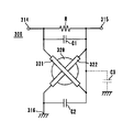
例えば、この種のアイソレータとして、特開平9−232818号公報記載のものが知られている。この2ポート型アイソレータの外観斜視図を図12に示し、電気等価回路図を図13に示す。このアイソレータ300は、金属製下側ケース301および金属製上側ケース302を接合して構成した金属ケース内に、永久磁石(図示せず)と、フェライト320と、フェライト320の主面に配置された第1中心電極321および第2中心電極322と、整合用コンデンサC1,C2と、抵抗Rとを収容している。第1および第2中心電極321,322と整合用コンデンサC1,C2と抵抗Rは積層基板330に内蔵され、積層基板330の表面には入力ポート314、出力ポート315およびアースポート316が設けられている。
【0004】
図示しないが、積層基板330の下面には、整合用コンデンサC1,C2の出力ポート315側共通コンデンサ電極が配設されている。この共通コンデンサ電極は金属製下側ケース301に電気的に接続されている。
【0005】
また、この2ポート型アイソレータ300を図12に示すように、携帯電話などのプリント基板350に実装すると、金属製下側ケース301とプリント基板350のアースパターンGとの間に若干の隙間が生じる。なぜなら、積層基板330に設けたポート314〜316を、プリント基板350の信号線路340,341やアースパターンGに確実にはんだ付けできるように、積層基板330の両側の足部分の底面が、金属製下側ケース301の底面より若干突出するように設計されているからである。
【0006】
【発明が解決しようとする課題】
ところが、従来の2ポート型アイソレータ300において、金属ケース(金属製下側ケース301)は、アースポート316に接続されておらず、電気的に浮いた状態であった。このため、金属ケースとプリント基板のアースパターンGとの間に浮遊容量が生じる。
【0007】
この浮遊容量C3は、等価回路で図13に示すように接続され、実質的には整合用コンデンサC2の静電容量が増えたことと等価である。このため、アイソレータ300の特性がずれ、アースパターンGの形状やアースパターンGと金属ケースとの隙間寸法によって特性がばらつくという問題があった。
【0008】
そこで、本発明の目的は、プリント基板等に実装した際にプリント基板のアースパターンとの間に生じる浮遊容量を抑えることができる2ポート型非可逆回路素子および通信装置を提供することにある。
【0009】
【課題を解決するための手段および作用】
前記目的を達成するため、本発明に係る2ポート型非可逆回路素子は、
(a)永久磁石と、
(b)永久磁石により直流磁界が印加されるフェライトと、
(c)フェライトの主面に配置され、一端が第1入出力ポートに電気的に接続され、他端が第2入出力ポートに電気的に接続されている第1中心電極と、
(d)第1中心電極と電気的絶縁状態で交差してフェライトの主面に配置され、一端が第2入出力ポートに電気的に接続され、他端がアースポートに電気的に接続されている第2中心電極と、
(e)第1入出力ポートと第2入出力ポートの間に電気的に接続された、第1整合用コンデンサと抵抗からなる並列RC回路と、
(f)第2入出力ポートとアースポートの間に電気的に接続された第2整合用コンデンサと、
(g)永久磁石とフェライトと第1および第2中心電極とを囲む金属ケースとを備え、
(h)金属ケースをアースポートに電気的に接続したこと、
を特徴とする。
【0010】
より具体的には、第1および第2整合用コンデンサが、複数の誘電体層とコンデンサ電極を積み重ねて構成した積層基板に内蔵され、該積層基板の上面にフェライトが配置されている。そして、金属ケースを、積層基板の下面に配設した第2整合用コンデンサのアース側コンデンサ電極に接合し、金属ケースをアースポートに電気的に接続している。
【0011】
以上の構成により、2ポート型非可逆回路素子をプリント基板等に実装すると、金属ケースは接地されて、第2整合用コンデンサのアース側コンデンサ電極やプリント基板のアースパターンと同電位になる。このため、金属ケースとプリント基板のアースパターンとの間に生じる浮遊容量が発生しにくくなる。さらに、アースポートを複数設けることにより、金属ケースをより一層確実かつ安定して接地できる。
【0012】
また、第2整合用コンデンサのアース側コンデンサ電極を複数の層に配置したり、第1整合用コンデンサの第1入出力ポートに電気的に接続された側のコンデンサ電極を複数の層に配置したりすることにより、第2整合用コンデンサや第1整合用コンデンサの静電容量を大きくできる。さらに、第1整合用コンデンサと第2整合用コンデンサを、積層基板の積み重ね方向において、異なる位置に配置することにより、第1および第2整合用コンデンサが異なる層に形成される。従って、1層あたりに形成できるコンデンサ電極を広面積にでき、静電容量が大きく、かつ、積層基板面積を有効利用した第1および第2整合用コンデンサが得られる。
【0013】
また、第1整合用コンデンサのコンデンサ電極の一つが積層基板の表層近傍に、第2整合用コンデンサのアース側コンデンサ電極の一つと同層に設けられている。これにより、第1および第2整合用コンデンサのトリミング調整が容易になる。
【0014】
また、第1中心電極と第2中心電極のそれぞれの両端部がフェライトの下面に延在し、第1中心電極の第2入出力ポートに電気的に接続された側の一端と第2中心電極の第2入出力ポートに電気的に接続された側の一端とがフェライトの下面で電気的に接続し、かつ、第1および第2中心電極のそれぞれの他端が相互に分離している。以上の構成により、中心電極と積層基板の電気的接続箇所が低減され、低コスト、かつ、高信頼性を実現できる。
【0015】
また、本発明に係る通信装置は、上述の2ポート型非可逆回路素子を備えることにより、性能や信頼性が向上する。
【0016】
【発明の実施の形態】
以下に、本発明に係る2ポート型非可逆回路素子および通信装置の実施の形態について添付の図面を参照して説明する。
【0017】
[第1実施形態、図1〜図8]
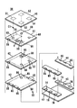
本発明に係る2ポート型非可逆回路素子の一実施形態の分解斜視図を図1に示す。該2ポート型非可逆回路素子1は、集中定数型アイソレータである。図1に示すように、2ポート型アイソレータ1は、概略、金属製上側ケース4と金属製下側ケース8とからなる金属ケースと、永久磁石9と、フェライト20と中心電極21,22とからなる中心電極組立体13と、積層基板30を備えている。
【0018】
金属製上側ケース4は略箱形状であり、上部4aおよび四つの側部4bからなる。金属製下側ケース8は、左右の側部8bと底部8aからなる。金属製上側ケース4および金属製下側ケース8は磁気回路を形成するため、例えば、軟鉄などの強磁性体からなる材料で形成され、その表面にAgやCuがめっきされる。
【0019】
中心電極組立体13は、円板状のマイクロ波フェライト20の上面に2組の第1および第2中心電極21,22を、絶縁層(図示せず)を介在させて直交して交差するように配置している。本第1実施形態では、中心電極21,22を二つのラインで構成した。第1中心電極21と第2中心電極22のそれぞれの両端部21a,21b、22a,22bは、フェライト20の下面に延在し、それぞれの端部21a〜22bが相互に分離している。
【0020】
中心電極21,22は銅箔を用いてフェライト20に巻きつけてもよいし、フェライト20上あるいは内部に銀ペーストを印刷して形成してもよい。あるいは、特開平9−232818号公報記載のように積層基板で形成されていてもよい。ただし、印刷した方が中心電極21,22の位置精度が高いので、積層基板30との接続が安定する。特に、今回のように微小な中心電極用接続電極51〜54(後述)で接続する場合には、中心電極21,22を印刷形成した方が信頼性、作業性が良い。
【0021】
積層基板30は、図2に示すように、中心電極用接続電極51〜54と、コンデンサ電極55や中継電極56や抵抗Rを裏面に設けた誘電体シート41と、コンデンサ電極57を裏面に設けた誘電体シート42と、グランド電極58を裏面に設けた誘電体シート43と、入力ポート14や出力ポート15やアースポート16を設けた誘電体シート45などにて構成されている。
【0022】
この積層基板30は、以下のようにして作製される。すなわち、誘電体シート41〜45は、Al2O3を主成分とし、SiO2,SrO,CaO,PbO,Na2O,K2O,MgO,BaO,CeO2,B2O3のうちの1種類あるいは複数種類を副成分として含む低温焼結誘電体材料にて作製する。
【0023】
さらに、積層基板30の焼成条件(特に焼成温度1000℃以下)では焼成せず、積層基板30の基板平面方向(X−Y方向)の焼成収縮を抑制する収縮抑制シート46,47を作製する。この収縮抑制シート46,47の材料は、アルミナ粉末および安定化ジルコニア粉末の混合材料である。シート41〜47の厚みは10μm〜200μm程度である。
【0024】
電極51〜58は、パターン印刷などの方法によりシート41〜43,46の裏面に形成される。電極51〜58の材料としては、抵抗率が低く、誘電体シート41〜45と同時焼成可能なAg,Cu,Ag−Pdなどが用いられる。この電極51〜58の表面には、Niめっきを下地としてAuめっきが施されている。Niめっきは、電極51〜58のAgとAuめっきの固着強度を強くする。Auめっきは、はんだ濡れ性を良くするとともに、導電率が高いのでアイソレータ1を低損失にできる。電極51〜58の厚みは2μm〜20μm程度である。通常、電極51〜58等の厚みは表皮厚の2倍以上に設定される。
【0025】
抵抗Rは、パターン印刷等の方法により誘電体シート41の裏面に形成される。抵抗Rの材料としては、サーメット、カーボン、ルテニウムなどが使用される。抵抗Rは積層基板30の上面に印刷で形成してもよいし、チップ抵抗で形成してもよい。
【0026】
ビアホール60や側面ビアホール65やポート14〜16は、誘電体シート41〜45にレーザ加工やパンチング加工などにより、予めビアホール用孔を形成した後、そのビアホール用孔に導電ペーストを充填することにより形成される。
【0027】
コンデンサ電極57は、誘電体シート42を間に挟んでコンデンサ電極55に対向して整合用コンデンサC1を構成する。さらに、コンデンサ電極57は、誘電体シート43を間に挟んでグランド電極58に対向して整合用コンデンサC2を構成する。これら整合用コンデンサC1,C2や抵抗Rは、電極51〜54やポート14〜16やビアホール60,65とともに、積層基板30の内部に電気回路を構成する。
【0028】
以上の誘電体シート41〜45は積層され、さらに、誘電体シート41〜45の積層体の上下両側から収縮抑制シート46,47で挟み込んだ後、焼成される。これにより、焼結体が得られ、その後、超音波洗浄法や湿式ホーニング法によって、未焼結の収縮抑制材料を除去し、図1に示すような積層基板30とする。
【0029】
積層基板30の両端部には、それぞれ入力ポート14、出力ポート15およびアースポート16が設けられている。入力ポート14はコンデンサ電極55に電気的に接続され、出力ポート15はコンデンサ電極57に電気的に接続されている。アースポート16は、グランド電極58に電気的に接続されている。
【0030】
なお、この積層基板30は、通常、マザーボード状態で作成される。このマザーボードに所定のピッチでハーフカット溝を形成し、ハーフカット溝に沿って折ることにより、マザーボードから所望のサイズの積層基板30を得る。あるいは、マザーボードをダイサーやレーザなどで切断することにより、所望のサイズの積層基板30を切り出してもよい。
【0031】
こうして得られた積層基板30は、内部に整合用コンデンサC1,C2および抵抗Rを有している。整合用コンデンサC1のトリミングは、整合用コンデンサC1,C2と中心電極21,22を接続する前に行なわれる。つまり、積層基板30は、単体の状態で、内部(2層目)のコンデンサ電極55を表層の誘電体とともにトリミング(削除)される。トリミングには、例えば、切削機やYAGの基本波、2倍波、3倍波のレーザが用いられる。レーザを用いれば、早くかつ精度の良い加工が得られる。なお、トリミングは、マザーボード状態の積層基板30に対して効率良く行ってもよい。
【0032】
このように、積層基板30の上面に近いコンデンサ電極55をトリミング用コンデンサ電極としているので、トリミング時に除去する誘電体層の厚みを最小限にできる。さらに、トリミングの障害となる電極が少なくなるので(本第1実施形態の場合は接続電極51〜54のみ)、トリミング可能なコンデンサ電極領域が広くなり、静電容量調整範囲を広くできる。
【0033】
また、積層基板30には抵抗Rも内蔵されており、整合用コンデンサC1と同様に抵抗Rも、表層の誘電体とともにトリミングすることにより、抵抗値を調整することができる。抵抗Rは1箇所でも幅が細くなると抵抗値が上がるので、幅方向の途中まで削る。
【0034】
以上の構成部品は以下のようにして組み立てられる。すなわち、図1に示すように、永久磁石9は金属製上側ケース4の天井に接着剤によって固定される。中心電極組立体13の中心電極21,22の各々の端部21a〜22bが積層基板30の表面に形成された中心電極用接続電極51〜54にはんだ80にて電気的に接続されることにより、積層基板30上に中心電極組立体13が実装される。なお、中心電極21,22と中心電極用接続電極51〜54のはんだ付けは、マザーボード状態の積層基板30に対して効率良く行ってもよい。
【0035】
積層基板30は金属製下側ケース8の底部8a上に載置され、積層基板30の下面に配設されているグランド電極58がはんだ80によって底部8aと接続固定される。これにより、アースポート16が底部8aに電気的に容易に接続される。
【0036】
そして、金属製下側ケース8と金属製上側ケース4は、それぞれの側部8bと4bをはんだ等で接合することにより金属ケースを構成し、ヨークとしても機能する。つまり、この金属ケースは、永久磁石9と中心電極組立体13と積層基板30を囲む磁路を形成する。また、永久磁石9はフェライト20に直流磁界を印加する。
【0037】
こうして、図3に示す2ポート型アイソレータ1が得られる。図4はアイソレータ1の電気等価回路図である。第1中心電極21の一端部21aは入力ポート14に電気的に接続され、他端部21bは出力ポート15に電気的に接続されている。第2中心電極22の一端部22aは出力ポート15に電気的に接続され、他端部22bはアースポート16に電気的に接続されている。整合用コンデンサC1と抵抗Rからなる並列RC回路は、入力ポート14と出力ポート15の間に電気的に接続されている。整合用コンデンサC2は出力ポート15とアースポート16の間に電気的に接続されている。
【0038】
以上の構成からなる2ポート型アイソレータ1は、金属製下側ケース8の底部8a(金属ケース)とアースポート16が電気的に接続しているので、図3に示すように、携帯電話などのプリント基板350に実装すると、金属ケースは接地されて、プリント基板350のアースパターンGと同電位になる。このため、金属ケースとアースパターンGとの間に生じる浮遊容量を抑えることができ、プリント基板350に実装したときの特性ずれや特性ばらつきが小さい2ポート型アイソレータ1を得ることができる。
【0039】
ここで、この2ポート型アイソレータ1を図3に示すように、携帯電話などのプリント基板350に実装すると、金属製下側ケース8とプリント基板350のアースパターンGとの間に若干の隙間が生じる。なぜなら、積層基板30に設けたポート14〜16を、プリント基板350の信号線路340,341やアースパターンGに確実にはんだ付けできるように、積層基板30の両側の足部分の底面が、金属製下側ケース8の底面より若干突出するように設計されているからである。また、はんだ付け部には、はんだ流れ防止のため、電極の上に絶縁層を設けてある。このため、例え端子部に突出がなくとも、プリント基板350のアースパターンGとアイソレータ1の間には絶縁層分の隙間が生じる。
【0040】
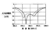
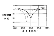
図5、図6、図7および図8はそれぞれ、縦4mm×横4mm×高さ1.7mmのサイズの2ポート型アイソレータ1の入力反射損失特性、出力反射損失特性、アイソレーション特性および挿入損失特性を示すグラフである(実線参照)。この2ポート型アイソレータ1をプリント基板350に実装した後も、これらの特性は殆ど変化しなかった。一方、図13に示す金属ケースとアースポート316が電気的に接続されていない従来の2ポート型アイソレータ300(サイズ:縦4mm×横4mm×高さ1.7mm)をプリント基板350に実装した場合には、特性ずれが生じた(点線参照)。このとき、金属ケースとプリント基板350のアースパターンGとの隙間寸法は0.1mmであった。つまり、厚みが0.1mmで、比誘電率1(空気)の浮遊容量(約1.4pF)が形成されている場合の特性である。
【0041】
また、本第1実施形態では、アースポート16を四つ設けている。これにより、金属ケースをより一層確実かつ安定して接地できるとともに、アイソレータ1の実装強度を向上できる。また、整合用コンデンサC1とC2を、積層基板30の積み重ね方向に上下に配置しているので、1層あたりに形成できる電極55,57,58を広面積にできる。従って、整合用コンデンサC1,C2のそれぞれの静電容量を大きくできる。
【0042】
[第2実施形態、図9および図10]
図9に示されている2ポート型アイソレータ1Aは、中心電極組立体13Aと積層基板30Aの他は前記第1実施形態の2ポート型アイソレータ1と同様のものである。
【0043】
中心電極組立体13Aは、フェライト20の上面に第1および第2中心電極21,22を、絶縁層(図示せず)を介在させて交差するように配置している。中心電極21,22のそれぞれの両端部21a〜22bは、フェライト20の下面に延在している。そして、第1中心電極21の出力ポート15に電気的に接続された側の端部21bと、第2中心電極22の入力ポート14に電気的に接続された側の端部22aとが、フェライト20の下面で電気的に接続している。中心電極21,22の残りの端部21a,22bは、相互に分離している。
【0044】
積層基板30Aは、図10に示すように、中心電極用接続電極51〜53と、コンデンサ電極55aやグランド電極59aや抵抗Rなどを裏面に設けた誘電体シート41aと、コンデンサ電極57aを裏面に設けた誘電体シート42aと、コンデンサ電極55bやグランド電極59bを裏面に設けた誘電体シート41bと、コンデンサ電極57bを裏面に設けた誘電体シート42bと、グランド電極58を裏面に設けた誘電体シート43と、入力ポート14や出力ポート15やアースポート16を設けた誘電体シート45などにて構成されている。
【0045】
コンデンサ電極57a,57bは、誘電体シート42a,41b,42bを間に挟んでコンデンサ電極55a,55bに対向して多段の整合用コンデンサC1を構成している。さらに、コンデンサ電極57a,57bは、誘電体シート42a,41b,42b,43を間に挟んでグランド電極59a,59b,58に対向して多段の整合用コンデンサC2を構成している。これにより、静電容量の大きい整合用コンデンサC1,C2を得ることができる。また、同じ静電容量であれば、電極面積を小さくできるので、コンデンサの導体損を低減でき、アイソレータ1Aの損失を低減できる。
【0046】
また、整合用コンデンサC2のグランド電極(アース側コンデンサ電極)59aは、積層基板30Aの表層近くに、整合用コンデンサC1のコンデンサ電極(入力ポート14に電気的に接続された側のコンデンサ電極)55aと同じ層(2層目)に配置されている。従って、グランド電極59aを表層の誘電体とともにトリミングすることにより、整合用コンデンサC2の静電容量を調整することができる。
【0047】
この積層基板30Aの上に中心電極組立体13Aが実装される。積層基板30Aは、表層に形成された中心電極用接続電極51〜53の数が少なく、積層基板30Aに形成するビアホール60の数や接続箇所を削減することができ、製造コストを低減することができる。
【0048】
[第3実施形態、図11]
第3実施形態は、本発明に係る通信装置として、携帯電話を例にして説明する。
【0049】
図11は携帯電話220のRF部分の電気回路ブロック図である。図11において、222はアンテナ素子、223はデュプレクサ、231は送信側アイソレータ、232は送信側増幅器、233は送信側段間用帯域通過フィルタ、234は送信側ミキサ、235は受信側増幅器、236は受信側段間用帯域通過フィルタ、237は受信側ミキサ、238は電圧制御発振器(VCO)、239はローカル用帯域通過フィルタである。
【0050】
ここに、送信側アイソレータ231として、前記第1および第2実施形態の集中定数型アイソレータ1,1Aを使用することができる。これらのアイソレータを実装することにより、電気的特性の向上した、かつ、信頼性の高い携帯電話を実現することができる。
【0051】
なお、本発明は前記実施形態に限定するものではなく、その要旨の範囲内で種々に変更することができる。
【0052】
【発明の効果】
以上の説明で明らかなように、本発明によれば、金属ケースをアースポートに電気的に接続したので、2ポート型非可逆回路素子をプリント基板等に実装すると、金属ケースは接地されて、第2整合用コンデンサのアース側コンデンサ電極やプリント基板のアースパターンと同電位になる。このため、金属ケースとプリント基板のアースパターンとの間に生じる浮遊容量を抑えることができ、プリント基板に実装したときの特性ずれや特性ばらつきを小さくできる。この結果、高性能で信頼性が高くかつ小型の2ポート型非可逆回路素子や通信装置を得ることができる。
【図面の簡単な説明】
【図1】本発明に係る2ポート型非可逆回路素子の一実施形態を示す分解斜視図。
【図2】図1に示した積層基板の分解斜視図。
【図3】図1に示した2ポート型非可逆回路素子の外観斜視図。
【図4】図1に示した2ポート型非可逆回路素子の電気等価回路図。
【図5】入力反射損失特性を示すグラフ。
【図6】出力反射損失特性を示すグラフ。
【図7】アイソレーション特性を示すグラフ。
【図8】挿入損失特性を示すグラフ。
【図9】本発明に係る2ポート型非可逆回路素子の別の実施形態を示す分解斜視図。
【図10】図9に示した積層基板の分解斜視図。
【図11】本発明に係る通信装置の電気回路ブロック図。
【図12】従来の2ポート型非可逆回路素子を示す外観斜視図。
【図13】図12に示した2ポート型非可逆回路素子の電気等価回路図。
【符号の説明】
1,1A…集中定数型アイソレータ
4…金属製上側ケース
8…金属製下側ケース
9…永久磁石
13,13A…中心電極組立体
14…入力ポート
15…出力ポート
16…アースポート
20…フェライト
21…第1中心電極
22…第2中心電極
21a,21b,22a,22b…端部
30,30A…積層基板
41〜45,41a,41b,42a,42b…誘電体シート
55,57,55a,55b,57a,57b…コンデンサ電極
58,59a,59b…グランド電極
220…携帯電話
C1,C2…整合用コンデンサ
R…抵抗[0001]
TECHNICAL FIELD OF THE INVENTION
The present invention relates to a two-port non-reciprocal circuit device, particularly to a two-port non-reciprocal circuit device such as an isolator used in a microwave band and a communication device.
[0002]
[Prior art]
Generally, an isolator has a function of passing a signal only in a transmission direction and preventing transmission in a reverse direction, and is used in a transmission circuit unit of a mobile communication device such as a car phone or a mobile phone.
[0003]
For example, a known isolator of this type is disclosed in Japanese Patent Application Laid-Open No. 9-232818. FIG. 12 is an external perspective view of the two-port isolator, and FIG. 13 is an electrical equivalent circuit diagram. The
[0004]
Although not shown, on the lower surface of the laminated
[0005]
When this two-
[0006]
[Problems to be solved by the invention]
However, in the conventional two-
[0007]
This stray capacitance C3 is connected in an equivalent circuit as shown in FIG. 13, and is substantially equivalent to an increase in the capacitance of the matching capacitor C2. For this reason, there is a problem that the characteristics of the
[0008]
SUMMARY OF THE INVENTION It is an object of the present invention to provide a two-port type non-reciprocal circuit device and a communication device capable of suppressing stray capacitance generated between the printed circuit board and a ground pattern when the device is mounted on a printed circuit board or the like.
[0009]
Means and action for solving the problem
In order to achieve the above object, a two-port non-reciprocal circuit device according to the present invention comprises:
(A) a permanent magnet;
(B) a ferrite to which a DC magnetic field is applied by a permanent magnet;
(C) a first center electrode disposed on the main surface of the ferrite, one end of which is electrically connected to the first input / output port, and the other end of which is electrically connected to the second input / output port;
(D) disposed on the main surface of the ferrite so as to intersect with the first center electrode in an electrically insulated state, one end of which is electrically connected to the second input / output port, and the other end of which is electrically connected to the ground port. A second central electrode,
(E) a parallel RC circuit comprising a first matching capacitor and a resistor, electrically connected between the first input / output port and the second input / output port;
(F) a second matching capacitor electrically connected between the second input / output port and the earth port;
(G) a metal case surrounding the permanent magnet, the ferrite, and the first and second center electrodes,
(H) electrically connecting the metal case to the earth port;
It is characterized by.
[0010]
More specifically, the first and second matching capacitors are built in a multilayer substrate formed by stacking a plurality of dielectric layers and capacitor electrodes, and ferrite is disposed on the upper surface of the multilayer substrate. Then, the metal case is joined to the earth-side capacitor electrode of the second matching capacitor provided on the lower surface of the multilayer substrate, and the metal case is electrically connected to the earth port.
[0011]
When the two-port type non-reciprocal circuit element is mounted on a printed circuit board or the like with the above configuration, the metal case is grounded and has the same potential as the ground-side capacitor electrode of the second matching capacitor and the ground pattern of the printed circuit board. For this reason, a stray capacitance generated between the metal case and the ground pattern of the printed board is less likely to occur. Further, by providing a plurality of ground ports, the metal case can be grounded more reliably and stably.
[0012]
Also, the ground-side capacitor electrode of the second matching capacitor may be arranged in a plurality of layers, or the capacitor electrode on the side electrically connected to the first input / output port of the first matching capacitor may be arranged in a plurality of layers. By doing so, the capacitance of the second matching capacitor and the first matching capacitor can be increased. Furthermore, by arranging the first matching capacitor and the second matching capacitor at different positions in the stacking direction of the multilayer substrate, the first and second matching capacitors are formed on different layers. Therefore, the capacitor electrodes that can be formed per layer can have a large area, the capacitance can be large, and the first and second matching capacitors that effectively utilize the area of the laminated substrate can be obtained.
[0013]
Also, one of the capacitor electrodes of the first matching capacitor is provided near the surface layer of the multilayer substrate and in the same layer as one of the ground-side capacitor electrodes of the second matching capacitor. This facilitates trimming adjustment of the first and second matching capacitors.
[0014]
Both ends of the first center electrode and the second center electrode extend on the lower surface of the ferrite, and one end of the first center electrode on the side electrically connected to the second input / output port and the second center electrode. One end on the side electrically connected to the second input / output port is electrically connected to the lower surface of the ferrite, and the other ends of the first and second center electrodes are separated from each other. With the above configuration, the number of electrical connections between the center electrode and the laminated substrate is reduced, and low cost and high reliability can be realized.
[0015]
Further, the communication device according to the present invention includes the above-described two-port type non-reciprocal circuit device, so that performance and reliability are improved.
[0016]
BEST MODE FOR CARRYING OUT THE INVENTION
Hereinafter, embodiments of a two-port type non-reciprocal circuit device and a communication device according to the present invention will be described with reference to the accompanying drawings.
[0017]
[First Embodiment, FIGS. 1 to 8]
FIG. 1 is an exploded perspective view of one embodiment of a two-port non-reciprocal circuit device according to the present invention. The two-port type
[0018]
The metal upper case 4 has a substantially box shape and includes an upper portion 4a and four
[0019]
The
[0020]
The
[0021]
As shown in FIG. 2, the
[0022]
This
[0023]
Furthermore,
[0024]
The
[0025]
The resistor R is formed on the back surface of the
[0026]
The via holes 60, the side via
[0027]
The
[0028]
The above-described
[0029]
An
[0030]
Note that the
[0031]
The
[0032]
As described above, since the
[0033]
The
[0034]
The above components are assembled as follows. That is, as shown in FIG. 1, the permanent magnet 9 is fixed to the ceiling of the metal upper case 4 by an adhesive. The respective ends 21 a to 22 b of the
[0035]
The
[0036]
The metal lower case 8 and the metal upper case 4 form a metal case by joining the
[0037]
Thus, the two-
[0038]
In the two-
[0039]
Here, as shown in FIG. 3, when this two-
[0040]
FIGS. 5, 6, 7, and 8 show the input reflection loss characteristic, output reflection loss characteristic, isolation characteristic, and insertion loss of the two-
[0041]
In the first embodiment, four
[0042]
[Second Embodiment, FIGS. 9 and 10]
The two-
[0043]
In the
[0044]
As shown in FIG. 10, the
[0045]
The
[0046]
The ground electrode (earth-side capacitor electrode) 59a of the matching capacitor C2 is located near the surface layer of the
[0047]
The
[0048]
[Third embodiment, FIG. 11]
In the third embodiment, a mobile phone will be described as an example of the communication device according to the present invention.
[0049]
FIG. 11 is an electric circuit block diagram of the RF portion of the
[0050]
Here, the lumped
[0051]
It should be noted that the present invention is not limited to the above embodiment, and can be variously modified within the scope of the gist.
[0052]
【The invention's effect】
As apparent from the above description, according to the present invention, since the metal case is electrically connected to the ground port, when the two-port type non-reciprocal circuit element is mounted on a printed circuit board or the like, the metal case is grounded, It has the same potential as the ground-side capacitor electrode of the second matching capacitor and the ground pattern of the printed circuit board. For this reason, the stray capacitance generated between the metal case and the ground pattern of the printed board can be suppressed, and the characteristic shift and the characteristic variation when mounted on the printed board can be reduced. As a result, it is possible to obtain a high-performance, highly-reliable and small two-port type non-reciprocal circuit device or communication device.
[Brief description of the drawings]
FIG. 1 is an exploded perspective view showing an embodiment of a two-port non-reciprocal circuit device according to the present invention.
FIG. 2 is an exploded perspective view of the laminated substrate shown in FIG.
FIG. 3 is an external perspective view of the two-port nonreciprocal circuit device shown in FIG.
FIG. 4 is an electrical equivalent circuit diagram of the two-port nonreciprocal circuit device shown in FIG.
FIG. 5 is a graph showing input return loss characteristics.
FIG. 6 is a graph showing output return loss characteristics.
FIG. 7 is a graph showing isolation characteristics.
FIG. 8 is a graph showing insertion loss characteristics.
FIG. 9 is an exploded perspective view showing another embodiment of the two-port type non-reciprocal circuit device according to the present invention.
10 is an exploded perspective view of the laminated substrate shown in FIG.
FIG. 11 is an electric circuit block diagram of a communication device according to the present invention.
FIG. 12 is an external perspective view showing a conventional two-port type non-reciprocal circuit device.
13 is an electrical equivalent circuit diagram of the two-port nonreciprocal circuit device shown in FIG.
[Explanation of symbols]
1, 1A Lumped constant type isolator 4 Metal upper case 8 Metal lower case 9
Claims (10)
前記永久磁石により直流磁界が印加されるフェライトと、
前記フェライトの主面に配置され、一端が第1入出力ポートに電気的に接続され、他端が第2入出力ポートに電気的に接続されている第1中心電極と、
前記第1中心電極と電気的絶縁状態で交差して前記フェライトの主面に配置され、一端が第2入出力ポートに電気的に接続され、他端がアースポートに電気的に接続されている第2中心電極と、
前記第1入出力ポートと前記第2入出力ポートの間に電気的に接続された、第1整合用コンデンサと抵抗からなる並列RC回路と、
前記第2入出力ポートと前記アースポートの間に電気的に接続された第2整合用コンデンサと、
前記永久磁石と前記フェライトと前記第1および第2中心電極とを囲む金属ケースとを備え、
前記金属ケースを前記アースポートに電気的に接続したこと、
を特徴とする2ポート型非可逆回路素子。A permanent magnet,
A ferrite to which a DC magnetic field is applied by the permanent magnet;
A first center electrode disposed on the main surface of the ferrite, one end of which is electrically connected to the first input / output port, and the other end of which is electrically connected to the second input / output port;
The ferrite is disposed on the main surface of the ferrite so as to intersect with the first center electrode in an electrically insulated state, one end is electrically connected to the second input / output port, and the other end is electrically connected to the ground port. A second center electrode;
A parallel RC circuit electrically connected between the first input / output port and the second input / output port, the parallel RC circuit including a first matching capacitor and a resistor;
A second matching capacitor electrically connected between the second input / output port and the ground port;
A metal case surrounding the permanent magnet, the ferrite, and the first and second center electrodes,
Electrically connecting the metal case to the ground port,
A two-port type non-reciprocal circuit device characterized by the above-mentioned.
Priority Applications (1)
| Application Number | Priority Date | Filing Date | Title |
|---|---|---|---|
| JP2002166186A JP3852373B2 (en) | 2002-06-06 | 2002-06-06 | Two-port nonreciprocal circuit device and communication device |
Applications Claiming Priority (1)
| Application Number | Priority Date | Filing Date | Title |
|---|---|---|---|
| JP2002166186A JP3852373B2 (en) | 2002-06-06 | 2002-06-06 | Two-port nonreciprocal circuit device and communication device |
Publications (2)
| Publication Number | Publication Date |
|---|---|
| JP2004015430A true JP2004015430A (en) | 2004-01-15 |
| JP3852373B2 JP3852373B2 (en) | 2006-11-29 |
Family
ID=30433841
Family Applications (1)
| Application Number | Title | Priority Date | Filing Date |
|---|---|---|---|
| JP2002166186A Expired - Fee Related JP3852373B2 (en) | 2002-06-06 | 2002-06-06 | Two-port nonreciprocal circuit device and communication device |
Country Status (1)
| Country | Link |
|---|---|
| JP (1) | JP3852373B2 (en) |
Cited By (4)
| Publication number | Priority date | Publication date | Assignee | Title |
|---|---|---|---|---|
| US7253697B2 (en) | 2004-07-30 | 2007-08-07 | Murata Manufacturing Co., Ltd. | Two-port isolator and communication apparatus |
| US8384490B2 (en) | 2008-04-18 | 2013-02-26 | Hitachi Metals, Ltd. | Non-reciprocal circuit and non-reciprocal circuit device, and central conductor assembly used therein |
| US8564380B2 (en) | 2007-01-30 | 2013-10-22 | Hitachi Metals, Ltd. | Non-reciprocal circuit device and its central conductor assembly |
| WO2018020801A1 (en) * | 2016-07-29 | 2018-02-01 | 株式会社村田製作所 | Irreversible circuit element, irreversible circuit module, front-end circuit and communication device |
-
2002
- 2002-06-06 JP JP2002166186A patent/JP3852373B2/en not_active Expired - Fee Related
Cited By (4)
| Publication number | Priority date | Publication date | Assignee | Title |
|---|---|---|---|---|
| US7253697B2 (en) | 2004-07-30 | 2007-08-07 | Murata Manufacturing Co., Ltd. | Two-port isolator and communication apparatus |
| US8564380B2 (en) | 2007-01-30 | 2013-10-22 | Hitachi Metals, Ltd. | Non-reciprocal circuit device and its central conductor assembly |
| US8384490B2 (en) | 2008-04-18 | 2013-02-26 | Hitachi Metals, Ltd. | Non-reciprocal circuit and non-reciprocal circuit device, and central conductor assembly used therein |
| WO2018020801A1 (en) * | 2016-07-29 | 2018-02-01 | 株式会社村田製作所 | Irreversible circuit element, irreversible circuit module, front-end circuit and communication device |
Also Published As
| Publication number | Publication date |
|---|---|
| JP3852373B2 (en) | 2006-11-29 |
Similar Documents
| Publication | Publication Date | Title |
|---|---|---|
| US6965276B2 (en) | Two port type isolator and communication device | |
| US20060022766A1 (en) | High frequency circuit module having non-reciprocal circuit element | |
| US6992540B2 (en) | Two-port isolator and communication device | |
| JP3835437B2 (en) | 2-port isolator and communication device | |
| US20080174381A1 (en) | Two-port isolator, characteristic adjusting method therefor, and communication apparatus | |
| JP4239916B2 (en) | 2-port isolator and communication device | |
| US6900704B2 (en) | Two-port isolator and communication device | |
| JP3858852B2 (en) | 2-port isolator and communication device | |
| JP3852373B2 (en) | Two-port nonreciprocal circuit device and communication device | |
| JP3705253B2 (en) | 3-port non-reciprocal circuit device and communication device | |
| JP4003650B2 (en) | Non-reciprocal circuit element, non-reciprocal circuit element mounting structure, and communication apparatus | |
| US6888432B2 (en) | Laminated substrate, method of producing the same, nonreciprocal circuit element, and communication device | |
| JP3829806B2 (en) | Multilayer substrate, multilayer substrate manufacturing method, non-reciprocal circuit device, and communication apparatus | |
| JP2004350164A (en) | Nonreversible circuit element, manufacturing method of nonreversible circuit element and communication device | |
| JP4293118B2 (en) | Non-reciprocal circuit device and communication device | |
| JP3948391B2 (en) | Non-reciprocal circuit device, manufacturing method thereof, and communication device | |
| JP2004023770A (en) | Irreversible circuit element and communication system | |
| JP4103755B2 (en) | Multilayer substrate, non-reciprocal circuit device and communication device | |
| JP2004296927A (en) | Wiring board for housing electronic component | |
| JP3979355B2 (en) | Multilayer substrate, multilayer substrate manufacturing method, non-reciprocal circuit device, and communication apparatus | |
| JP3852434B2 (en) | Non-reciprocal circuit device and communication device | |
| JP4631754B2 (en) | Non-reciprocal circuit device and communication device | |
| JPH1098315A (en) | Dielectric laminated device, its manufacture and mobile communication equipment | |
| JP2004193904A (en) | Two-port isolator and its manufacturing method and communication apparatus | |
| JP2002335105A (en) | Central conductor assembly and nonreversible circuit element using the same |
Legal Events
| Date | Code | Title | Description |
|---|---|---|---|
| A621 | Written request for application examination |
Free format text: JAPANESE INTERMEDIATE CODE: A621 Effective date: 20050510 |
|
| A131 | Notification of reasons for refusal |
Free format text: JAPANESE INTERMEDIATE CODE: A131 Effective date: 20060704 |
|
| A521 | Request for written amendment filed |
Free format text: JAPANESE INTERMEDIATE CODE: A523 Effective date: 20060720 |
|
| TRDD | Decision of grant or rejection written | ||
| A01 | Written decision to grant a patent or to grant a registration (utility model) |
Free format text: JAPANESE INTERMEDIATE CODE: A01 Effective date: 20060815 |
|
| A61 | First payment of annual fees (during grant procedure) |
Free format text: JAPANESE INTERMEDIATE CODE: A61 Effective date: 20060828 |
|
| R150 | Certificate of patent or registration of utility model |
Ref document number: 3852373 Country of ref document: JP Free format text: JAPANESE INTERMEDIATE CODE: R150 Free format text: JAPANESE INTERMEDIATE CODE: R150 |
|
| FPAY | Renewal fee payment (event date is renewal date of database) |
Free format text: PAYMENT UNTIL: 20090915 Year of fee payment: 3 |
|
| FPAY | Renewal fee payment (event date is renewal date of database) |
Free format text: PAYMENT UNTIL: 20100915 Year of fee payment: 4 |
|
| FPAY | Renewal fee payment (event date is renewal date of database) |
Free format text: PAYMENT UNTIL: 20100915 Year of fee payment: 4 |
|
| FPAY | Renewal fee payment (event date is renewal date of database) |
Free format text: PAYMENT UNTIL: 20110915 Year of fee payment: 5 |
|
| FPAY | Renewal fee payment (event date is renewal date of database) |
Free format text: PAYMENT UNTIL: 20120915 Year of fee payment: 6 |
|
| FPAY | Renewal fee payment (event date is renewal date of database) |
Free format text: PAYMENT UNTIL: 20120915 Year of fee payment: 6 |
|
| FPAY | Renewal fee payment (event date is renewal date of database) |
Free format text: PAYMENT UNTIL: 20130915 Year of fee payment: 7 |
|
| LAPS | Cancellation because of no payment of annual fees |