EP4579699A2 - Mehrschichtiges elektronisches bauteil mit einem riss, der sich von einem ende einer der äusseren elektroden in das innere des körpers erstreckt - Google Patents
Mehrschichtiges elektronisches bauteil mit einem riss, der sich von einem ende einer der äusseren elektroden in das innere des körpers erstreckt Download PDFInfo
- Publication number
- EP4579699A2 EP4579699A2 EP24210833.0A EP24210833A EP4579699A2 EP 4579699 A2 EP4579699 A2 EP 4579699A2 EP 24210833 A EP24210833 A EP 24210833A EP 4579699 A2 EP4579699 A2 EP 4579699A2
- Authority
- EP
- European Patent Office
- Prior art keywords
- overlapping region
- electronic component
- multilayer electronic
- electrode
- internal electrode
- Prior art date
- Legal status (The legal status is an assumption and is not a legal conclusion. Google has not performed a legal analysis and makes no representation as to the accuracy of the status listed.)
- Pending
Links
Images


Classifications
-
- H—ELECTRICITY
- H01—ELECTRIC ELEMENTS
- H01G—CAPACITORS; CAPACITORS, RECTIFIERS, DETECTORS, SWITCHING DEVICES, LIGHT-SENSITIVE OR TEMPERATURE-SENSITIVE DEVICES OF THE ELECTROLYTIC TYPE
- H01G4/00—Fixed capacitors; Processes of their manufacture
- H01G4/30—Stacked capacitors
-
- H—ELECTRICITY
- H01—ELECTRIC ELEMENTS
- H01G—CAPACITORS; CAPACITORS, RECTIFIERS, DETECTORS, SWITCHING DEVICES, LIGHT-SENSITIVE OR TEMPERATURE-SENSITIVE DEVICES OF THE ELECTROLYTIC TYPE
- H01G2/00—Details of capacitors not covered by a single one of groups H01G4/00-H01G11/00
- H01G2/02—Mountings
- H01G2/06—Mountings specially adapted for mounting on a printed-circuit support
-
- H—ELECTRICITY
- H01—ELECTRIC ELEMENTS
- H01G—CAPACITORS; CAPACITORS, RECTIFIERS, DETECTORS, SWITCHING DEVICES, LIGHT-SENSITIVE OR TEMPERATURE-SENSITIVE DEVICES OF THE ELECTROLYTIC TYPE
- H01G4/00—Fixed capacitors; Processes of their manufacture
- H01G4/002—Details
- H01G4/005—Electrodes
- H01G4/008—Selection of materials
- H01G4/0085—Fried electrodes
-
- H—ELECTRICITY
- H01—ELECTRIC ELEMENTS
- H01G—CAPACITORS; CAPACITORS, RECTIFIERS, DETECTORS, SWITCHING DEVICES, LIGHT-SENSITIVE OR TEMPERATURE-SENSITIVE DEVICES OF THE ELECTROLYTIC TYPE
- H01G4/00—Fixed capacitors; Processes of their manufacture
- H01G4/002—Details
- H01G4/005—Electrodes
- H01G4/012—Form of non-self-supporting electrodes
-
- H—ELECTRICITY
- H01—ELECTRIC ELEMENTS
- H01G—CAPACITORS; CAPACITORS, RECTIFIERS, DETECTORS, SWITCHING DEVICES, LIGHT-SENSITIVE OR TEMPERATURE-SENSITIVE DEVICES OF THE ELECTROLYTIC TYPE
- H01G4/00—Fixed capacitors; Processes of their manufacture
- H01G4/002—Details
- H01G4/228—Terminals
-
- H—ELECTRICITY
- H01—ELECTRIC ELEMENTS
- H01G—CAPACITORS; CAPACITORS, RECTIFIERS, DETECTORS, SWITCHING DEVICES, LIGHT-SENSITIVE OR TEMPERATURE-SENSITIVE DEVICES OF THE ELECTROLYTIC TYPE
- H01G4/00—Fixed capacitors; Processes of their manufacture
- H01G4/002—Details
- H01G4/228—Terminals
- H01G4/232—Terminals electrically connecting two or more layers of a stacked or rolled capacitor
-
- H—ELECTRICITY
- H01—ELECTRIC ELEMENTS
- H01G—CAPACITORS; CAPACITORS, RECTIFIERS, DETECTORS, SWITCHING DEVICES, LIGHT-SENSITIVE OR TEMPERATURE-SENSITIVE DEVICES OF THE ELECTROLYTIC TYPE
- H01G4/00—Fixed capacitors; Processes of their manufacture
- H01G4/002—Details
- H01G4/018—Dielectrics
- H01G4/06—Solid dielectrics
- H01G4/08—Inorganic dielectrics
- H01G4/12—Ceramic dielectrics
- H01G4/1209—Ceramic dielectrics characterised by the ceramic dielectric material
- H01G4/1218—Ceramic dielectrics characterised by the ceramic dielectric material based on titanium oxides or titanates
- H01G4/1227—Ceramic dielectrics characterised by the ceramic dielectric material based on titanium oxides or titanates based on alkaline earth titanates
Definitions
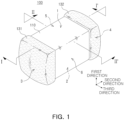
- the present disclosure relates to a multilayer electronic component.
- MLCCs may include a body and an external electrode disposed on the body.
- the stress tends to be concentrated on an end of the external electrode, and accordingly, a crack may occur from end of the external electrode toward the inside of the body.
- a short circuit may occur in the MLCC.
- a method of reducing the number of laminated internal electrodes or reducing a size of the overlapping region may be considered, but reducing the number of laminated internal electrodes or the size of the overlapping region may lower capacitance of an MLCC and DC-bias properties.
- an MLCC having excellent electrical properties such as capacitance and DC-bias while preventing short circuits from occurring due to a crack propagating to an overlapping region of a body.
- Another aspect of the present disclosure provides a multilayer electronic component having excellent electrical properties such as capacitance or the like.
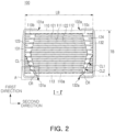
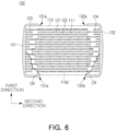
- the body may include an overlapping region in which the first internal electrode overlaps the second internal electrode adjacent thereto in the first direction with the dielectric layer interposed therebetween.
- a length in the second direction of a central portion of the overlapping region in the first direction may be greater than that of both ends of the overlapping region in the first direction.
- the body may have a crack extending to the inside of the body from an end of at least one of the first and second external electrodes, the crack spaced apart from the overlapping region.
- the multilayer electronic component 100 has a structure in which the central portion of the overlapping region 110a in the first direction, having a longer distance from the crack CR, has a length in the second direction longer than that of both ends of the overlapping region 110a, having a shorter distance from the crack CR, thereby preventing the crack CR from propagating to the inside of the overlapping region 110a to prevent a short circuit defect from occurring, and improving capacitance and DC-bias properties of the multilayer electronic component 100 as compared to a case in which an overall length of the overlapping region 110a in the second direction is reduced.
- a length in the second direction in which the first external electrode 131 and the second internal electrode 122 are spaced apart from each other may gradually increase from the central portion of the overlapping region 110a in the first direction to both ends of the overlapping region 110a in the first direction
- a length in the second direction in which the second external electrode 132 and the first internal electrode 121 are spaced apart from each other may gradually increase from the central portion of the overlapping region 110a in the first direction to both ends of the overlapping region 110a in the first direction.
- a distance in the second direction between the overlapping region 110a and the crack CR may gradually increase from both ends of the overlapping region 110a in the first direction toward the central portion of the overlapping region 110a in the first direction, but the present disclosure is not limited thereto.
- the crack CR propagating from the ends 131a and 132a of the external electrodes to the inside of the body 110, may easily occur as high pressure is applied to the multilayer electronic component 100.
- LE is shorter than the LM in order to prevent a short circuit defect from occurring due to the crack CR from extending to the inside of the overlapping region 110a, flexural strength of a high-pressure electronic component may not be ensured.
- the crack surface may be the second surface.
- One end of the crack CR, present on the end 131a of the first external electrode, may be positioned on the second surface, and the other end of the crack CR may be positioned on the third surface 3.
- ⁇ may be, for example, 60° to 70°.
- the body 110 may include a first dummy electrode 123 disposed to be spaced apart from the second internal electrode 122 in the second direction, the first dummy electrode 123 connected to the first external electrode 131, and a second dummy electrode 124 disposed to be spaced apart from the first internal electrode 121 in the second direction, the second dummy electrode 124 connected to the second external electrode 132.
- the first dummy electrode 123 may be substantially coplanar with the second internal electrode 122
- the second dummy electrode 124 may be substantially coplanar with the first internal electrode 121.
- the dummy electrodes 123 and 124 may be appropriately formed on the body 110, such that a multilayer electronic component according to an example embodiment of the present disclosure may be manufactured without increasing a type of internal electrode pattern printed on a ceramic green sheet to be described below.
- a length of the first dummy electrode 123 in the second direction, measured in the central portion of the overlapping region 110a in the first direction may be shorter than a length of the first dummy electrode 123 in the second direction, measured in both ends of the overlapping region 110a in the first direction.
- a length of the second dummy electrode 124 in the second direction, measured in the central portion of the overlapping region 110a in the first direction may be shorter than a length of the second dummy electrode 124 in the second direction, measured in both ends of the overlapping region 110a in the first direction.
- the length of the first dummy electrode 123 in the second direction may increase from a center of the body 110 in the first direction toward an outer portion of the body 110 in the first direction
- the length of the second dummy electrode 124 in the second direction may increase from the center of the body 110 in the first direction toward the outer portion of the body 110 in the first direction
- a gap between the first dummy electrode 123 and the second internal electrode 122 in the second direction may be substantially constant from a topmost first dummy electrode to a bottommost first dummy electrode.
- a gap between the second dummy electrode 124 and the first internal electrode 121 in the second direction may be substantially constant from a topmost second dummy electrode to a bottommost second dummy electrode.
- a ratio (LD/LM) of LD to LM may be 0.3 or more.
- LD/LM is less than 0.3, the second internal electrode 122 and the first dummy electrode 123 may come into contact with each other to cause a short circuit defect.
- An upper limit of LD/LM is not particularly limited, but may be 0.8 or less.
- ceramic powder particles for forming ceramic green sheets 211a and 211b may be prepared.
- the ceramic powder particles may be (Ba 1-x Ca x )TiO 3 (0 ⁇ x ⁇ 1), Ba(Ti 1-y Ca y )O 3 (0 ⁇ y ⁇ 1), (Ba 1-x Ca x )(Ti 1-y Zr y )O 3 (0 ⁇ x ⁇ 1, 0 ⁇ y ⁇ 1), or Ba (Ti 1-y Zr y )O 3 (0 ⁇ y ⁇ 1) obtained by partially dissolving Ca or Zr in BaTiO 3 .
- BaTiO 3 powder particles may be synthesized, for example, by reacting a titanium raw material such as titanium dioxide with a barium raw material such as barium carbonate.
- a method of synthesizing the ceramic powder particles may include, for example, a solid-phase method, a sol-gel method, and a hydrothermal synthesis method, but the present disclosure is not limited thereto.
- the prepared ceramic powder particles may be dried and ground, an organic solvent such as ethanol and a binder such as polyvinyl butyral may be mixed to prepare a ceramic slurry, and then the ceramic slurry may be coated and dried on a carrier film to prepare the ceramic green sheets 211a and 211b.
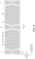
- the internal electrode patterns 221 and 222 may be formed on the ceramic green sheets 211a and 211b by printing a conductive paste for an internal electrode, including metal powder particles, a binder, an organic solvent or the like, to have a predetermined thickness using a screen-printing method, a gravure-printing method, or the like. More specifically, a plurality of first internal electrode patterns 221 may be formed on a first ceramic green sheet 211a, and a plurality of second internal electrode patterns 222 may be formed on a second ceramic green sheet 211b.
- the ceramic green sheets 211a and 211b on which the internal electrode patterns 221 and 222 are printed may be peeled off from the carrier film.
- the first ceramic green sheet 211a on which the first internal electrode pattern 221 is formed and the second ceramic green sheet 211b on which the second internal electrode pattern is formed may be alternately laminated to correspond to a predetermined number of layers and then compressed to form a ceramic laminate 200 illustrated in FIG. 5 .
- a ceramic green sheet on which an internal electrode pattern is not formed may be laminated on upper and lower portions of the ceramic laminate 200 to correspond to a predetermined number of layers to form the cover portions 112 and 113 on which sintering has been performed.
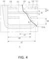
- the ceramic laminate 200 may be cut along a cutting line C1 to have a predetermined chip size, and the cut chip may be sintered at a temperature, for example, greater than or equal to 1000°C and less than or equal to 1400°C to form the body 110.
- a length D1 in which an end of the first internal electrode pattern is offset with respect to the cutting line C1 increases from a central portion of the ceramic laminate 200 in the first direction toward both ends of the ceramic laminate 200 in the first direction.
- a length D2 in which an end of the second internal electrode pattern is offset with respect to the cutting line C1 increases from the central portion of the ceramic laminate 200 in the first direction toward both ends of the ceramic laminate 200 in the first direction.
- the length in the second direction of the central portion of the overlapping region 110a in the first direction on which sintering has been performed may be greater than that of both ends of the overlapping region 110a in the first direction.
- the margin portions 114 and 115 may be formed by coating a ceramic green sheet with a conductive paste for an internal electrode, except for a portion of the ceramic green sheet on which a margin portion is to be formed.
- the ceramic laminate may be cut such that the internal electrode pattern is exposed on both surfaces of the cut chip in the third direction, and then the sheet for forming the margin portions may be attached to both surfaces of the cut chip in the third direction, and then sintered to form the margin portions 114 and 115.
- the body 110 may be dipped in a conductive paste including metal powder particles, a glass frit, a binder, and an organic solvent, and then the conductive paste may be sintered to form a base electrode layer.
- the base electrode layer includes a first layer including a metal and glass, and a second layer including a metal and a resin
- the second layer may be formed on the first layer by dipping in a conductive resin composition including metal powder particles, a resin, a binder, and an organic solvent, and then performing curing heat treatment at a temperature of 250°C to 550°C.
- the multilayer electronic component 100 may be manufactured by forming a plating layer using an electroplating method and/or an electroless plating method.
- a crack CR extending from an end of the external electrode to the inside of the body 110 may be formed by flexural stress applied to the multilayer electronic component 100.
- the length in the second direction of the central portion of the overlapping region 110a in the first direction may be greater than that of both ends of the overlapping region 110a in the first direction, such that the crack CR may be spaced apart from the overlapping region 110a.
- the above-described manufacturing method is an example, and the method of manufacturing the multilayer electronic component 100 is not limited to the above-described manufacturing method.
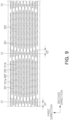
- a length of an overlapping region 110a' in the second direction may decrease in a stepwise manner from a central portion of the overlapping region 110a' in the first direction toward both ends of the overlapping region 110a' in the first direction.
- the multilayer electronic component 100' may have a structure in which the length of the overlapping region 110a' in the second direction decreases in a stepwise manner from the central portion of the overlapping region 110a' in the first direction to both ends of the overlapping region 110a' in the first direction, thereby preventing a crack CR from propagating to the inside of the overlapping region 110a' to prevent a short circuit defect from occurring, and improving capacitance and DC-bias properties of the multilayer electronic component 100' as compared to a case in which an overall length of the overlapping region 110a' in the second direction is reduced.
- FIG. 8 is a schematic cross-sectional view of a multilayer electronic component 100" according to another example embodiment of the present disclosure, and corresponds to FIG. 2 .
- FIG. 9 is a schematic cross-sectional view of a ceramic laminate 200" for manufacturing the multilayer electronic component 100" illustrated in FIG. 8 , and corresponds to FIG. 5 .
- FIGS. 8 and 9 a multilayer electronic component 100'' and a ceramic laminate 200" for manufacturing the multilayer electronic component 100" according to another example embodiment of the present disclosure will be described with reference to FIGS. 8 and 9 .
- the same/similar reference numerals are used for components the same as/similar to those of the multilayer electronic component 100 and the ceramic laminate 200 illustrated in FIGS. 1 to 5 , and thus repeated descriptions will be omitted.
Landscapes
- Engineering & Computer Science (AREA)
- Power Engineering (AREA)
- Microelectronics & Electronic Packaging (AREA)
- Manufacturing & Machinery (AREA)
- Chemical & Material Sciences (AREA)
- Materials Engineering (AREA)
- Fixed Capacitors And Capacitor Manufacturing Machines (AREA)
- Ceramic Capacitors (AREA)
- Ceramic Engineering (AREA)
- Inorganic Chemistry (AREA)
- Production Of Multi-Layered Print Wiring Board (AREA)
Applications Claiming Priority (1)
| Application Number | Priority Date | Filing Date | Title |
|---|---|---|---|
| KR1020230192398A KR20250101118A (ko) | 2023-12-27 | 2023-12-27 | 적층형 전자 부품 |
Publications (2)
| Publication Number | Publication Date |
|---|---|
| EP4579699A2 true EP4579699A2 (de) | 2025-07-02 |
| EP4579699A3 EP4579699A3 (de) | 2025-11-12 |
Family
ID=93430460
Family Applications (1)
| Application Number | Title | Priority Date | Filing Date |
|---|---|---|---|
| EP24210833.0A Pending EP4579699A3 (de) | 2023-12-27 | 2024-11-05 | Mehrschichtiges elektronisches bauteil mit einem riss, der sich von einem ende einer der äusseren elektroden in das innere des körpers erstreckt |
Country Status (5)
| Country | Link |
|---|---|
| US (1) | US20250218668A1 (de) |
| EP (1) | EP4579699A3 (de) |
| JP (1) | JP2025104268A (de) |
| KR (1) | KR20250101118A (de) |
| CN (1) | CN120221281A (de) |
Family Cites Families (5)
| Publication number | Priority date | Publication date | Assignee | Title |
|---|---|---|---|---|
| JP2002299148A (ja) * | 2001-03-30 | 2002-10-11 | Kyocera Corp | 積層セラミックコンデンサ及びその製造方法 |
| KR20150019643A (ko) * | 2013-08-14 | 2015-02-25 | 삼성전기주식회사 | 적층 세라믹 커패시터 |
| KR101792385B1 (ko) * | 2016-01-21 | 2017-11-01 | 삼성전기주식회사 | 적층 세라믹 커패시터 및 그 실장 기판 |
| KR102834093B1 (ko) * | 2020-09-18 | 2025-07-15 | 삼성전기주식회사 | 적층형 전자 부품 |
| KR102880989B1 (ko) * | 2020-12-09 | 2025-11-04 | 삼성전기주식회사 | 적층형 전자 부품 |
-
2023
- 2023-12-27 KR KR1020230192398A patent/KR20250101118A/ko active Pending
-
2024
- 2024-11-05 EP EP24210833.0A patent/EP4579699A3/de active Pending
- 2024-11-18 US US18/951,524 patent/US20250218668A1/en active Pending
- 2024-11-25 JP JP2024204403A patent/JP2025104268A/ja active Pending
- 2024-12-26 CN CN202411931607.1A patent/CN120221281A/zh active Pending
Also Published As
| Publication number | Publication date |
|---|---|
| KR20250101118A (ko) | 2025-07-04 |
| US20250218668A1 (en) | 2025-07-03 |
| JP2025104268A (ja) | 2025-07-09 |
| CN120221281A (zh) | 2025-06-27 |
| EP4579699A3 (de) | 2025-11-12 |
Similar Documents
| Publication | Publication Date | Title |
|---|---|---|
| US11735374B2 (en) | Multi-layered ceramic electronic component | |
| US11476047B2 (en) | Multilayer electronic component | |
| US11961673B2 (en) | Multilayer ceramic capacitor | |
| CN110942913A (zh) | 陶瓷电子组件 | |
| CN116844861A (zh) | 多层电子组件 | |
| EP4542598A1 (de) | Mehrschichtiges elektronisches bauteil | |
| US20250054692A1 (en) | Multilayer electronic component | |
| EP4579699A2 (de) | Mehrschichtiges elektronisches bauteil mit einem riss, der sich von einem ende einer der äusseren elektroden in das innere des körpers erstreckt | |
| EP4401104A2 (de) | Mehrschichtiges elektronisches bauteil | |
| US12278056B2 (en) | Multilayer electronic component | |
| US12374496B2 (en) | Multilayer electronic component | |
| KR20240147249A (ko) | 적층형 전자 부품 | |
| CN111009415A (zh) | 陶瓷电子组件 | |
| US20250210260A1 (en) | Multilayer electronic component | |
| CN116417260A (zh) | 多层电子组件 | |
| US20250118492A1 (en) | Multilayer electronic component | |
| EP4560666A1 (de) | Mehrschichtiges elektronisches bauteil | |
| US12198860B2 (en) | Multilayer electronic component and method of manufacturing the same | |
| EP4579700A1 (de) | Mehrschichtiges elektronisches bauteil | |
| EP4576136A1 (de) | Mehrschichtiges elektronisches bauteil | |
| EP4579698A2 (de) | Mehrschichtiges elektronisches bauteil mit verstärkungsmustern oder kurzen dummy-elektroden zur vermeidung von rissen in den ecken | |
| US20250087421A1 (en) | Multilayer electronic component | |
| JP2025105544A (ja) | 積層型電子部品 | |
| JP2026000838A (ja) | 積層型電子部品 |
Legal Events
| Date | Code | Title | Description |
|---|---|---|---|
| PUAI | Public reference made under article 153(3) epc to a published international application that has entered the european phase |
Free format text: ORIGINAL CODE: 0009012 |
|
| STAA | Information on the status of an ep patent application or granted ep patent |
Free format text: STATUS: THE APPLICATION HAS BEEN PUBLISHED |
|
| AK | Designated contracting states |
Kind code of ref document: A2 Designated state(s): AL AT BE BG CH CY CZ DE DK EE ES FI FR GB GR HR HU IE IS IT LI LT LU LV MC ME MK MT NL NO PL PT RO RS SE SI SK SM TR |
|
| PUAL | Search report despatched |
Free format text: ORIGINAL CODE: 0009013 |
|
| AK | Designated contracting states |
Kind code of ref document: A3 Designated state(s): AL AT BE BG CH CY CZ DE DK EE ES FI FR GB GR HR HU IE IS IT LI LT LU LV MC ME MK MT NL NO PL PT RO RS SE SI SK SM TR |
|
| RIC1 | Information provided on ipc code assigned before grant |
Ipc: H01G 4/008 20060101AFI20251007BHEP Ipc: H01G 4/012 20060101ALI20251007BHEP Ipc: H01G 4/12 20060101ALI20251007BHEP Ipc: H01G 4/232 20060101ALI20251007BHEP Ipc: H01G 4/30 20060101ALI20251007BHEP |