EP4579698A2 - Mehrschichtiges elektronisches bauteil mit verstärkungsmustern oder kurzen dummy-elektroden zur vermeidung von rissen in den ecken - Google Patents
Mehrschichtiges elektronisches bauteil mit verstärkungsmustern oder kurzen dummy-elektroden zur vermeidung von rissen in den ecken Download PDFInfo
- Publication number
- EP4579698A2 EP4579698A2 EP24219130.2A EP24219130A EP4579698A2 EP 4579698 A2 EP4579698 A2 EP 4579698A2 EP 24219130 A EP24219130 A EP 24219130A EP 4579698 A2 EP4579698 A2 EP 4579698A2
- Authority
- EP
- European Patent Office
- Prior art keywords
- reinforcing pattern
- length
- electronic component
- formation portion
- capacitance formation
- Prior art date
- Legal status (The legal status is an assumption and is not a legal conclusion. Google has not performed a legal analysis and makes no representation as to the accuracy of the status listed.)
- Pending
Links
Images


Classifications
-
- H—ELECTRICITY
- H01—ELECTRIC ELEMENTS
- H01G—CAPACITORS; CAPACITORS, RECTIFIERS, DETECTORS, SWITCHING DEVICES, LIGHT-SENSITIVE OR TEMPERATURE-SENSITIVE DEVICES OF THE ELECTROLYTIC TYPE
- H01G4/00—Fixed capacitors; Processes of their manufacture
- H01G4/002—Details
- H01G4/005—Electrodes
- H01G4/012—Form of non-self-supporting electrodes
-
- H—ELECTRICITY
- H01—ELECTRIC ELEMENTS
- H01G—CAPACITORS; CAPACITORS, RECTIFIERS, DETECTORS, SWITCHING DEVICES, LIGHT-SENSITIVE OR TEMPERATURE-SENSITIVE DEVICES OF THE ELECTROLYTIC TYPE
- H01G4/00—Fixed capacitors; Processes of their manufacture
- H01G4/002—Details
- H01G4/005—Electrodes
-
- H—ELECTRICITY
- H01—ELECTRIC ELEMENTS
- H01G—CAPACITORS; CAPACITORS, RECTIFIERS, DETECTORS, SWITCHING DEVICES, LIGHT-SENSITIVE OR TEMPERATURE-SENSITIVE DEVICES OF THE ELECTROLYTIC TYPE
- H01G4/00—Fixed capacitors; Processes of their manufacture
- H01G4/002—Details
- H01G4/005—Electrodes
- H01G4/008—Selection of materials
-
- H—ELECTRICITY
- H01—ELECTRIC ELEMENTS
- H01G—CAPACITORS; CAPACITORS, RECTIFIERS, DETECTORS, SWITCHING DEVICES, LIGHT-SENSITIVE OR TEMPERATURE-SENSITIVE DEVICES OF THE ELECTROLYTIC TYPE
- H01G4/00—Fixed capacitors; Processes of their manufacture
- H01G4/002—Details
- H01G4/018—Dielectrics
- H01G4/06—Solid dielectrics
- H01G4/08—Inorganic dielectrics
- H01G4/12—Ceramic dielectrics
-
- H—ELECTRICITY
- H01—ELECTRIC ELEMENTS
- H01G—CAPACITORS; CAPACITORS, RECTIFIERS, DETECTORS, SWITCHING DEVICES, LIGHT-SENSITIVE OR TEMPERATURE-SENSITIVE DEVICES OF THE ELECTROLYTIC TYPE
- H01G4/00—Fixed capacitors; Processes of their manufacture
- H01G4/002—Details
- H01G4/228—Terminals
- H01G4/232—Terminals electrically connecting two or more layers of a stacked or rolled capacitor
-
- H—ELECTRICITY
- H01—ELECTRIC ELEMENTS
- H01G—CAPACITORS; CAPACITORS, RECTIFIERS, DETECTORS, SWITCHING DEVICES, LIGHT-SENSITIVE OR TEMPERATURE-SENSITIVE DEVICES OF THE ELECTROLYTIC TYPE
- H01G4/00—Fixed capacitors; Processes of their manufacture
- H01G4/30—Stacked capacitors
-
- H—ELECTRICITY
- H01—ELECTRIC ELEMENTS
- H01G—CAPACITORS; CAPACITORS, RECTIFIERS, DETECTORS, SWITCHING DEVICES, LIGHT-SENSITIVE OR TEMPERATURE-SENSITIVE DEVICES OF THE ELECTROLYTIC TYPE
- H01G4/00—Fixed capacitors; Processes of their manufacture
- H01G4/002—Details
- H01G4/018—Dielectrics
- H01G4/06—Solid dielectrics
- H01G4/08—Inorganic dielectrics
- H01G4/12—Ceramic dielectrics
- H01G4/1209—Ceramic dielectrics characterised by the ceramic dielectric material
- H01G4/1218—Ceramic dielectrics characterised by the ceramic dielectric material based on titanium oxides or titanates
- H01G4/1227—Ceramic dielectrics characterised by the ceramic dielectric material based on titanium oxides or titanates based on alkaline earth titanates
Definitions
- the present disclosure relates to a multilayer electronic component.
- Multilayer ceramic capacitors are chip-type condensers mounted on the printed circuit boards of various electronic products including display devices, such as liquid crystal displays (LCDs) and plasma display panels (PDPs), computers, smartphones, cell phones, circuits, such as on-board charger (OBC) DC-DC converters of electric vehicles, and the like, to charge or discharge electricity.
- display devices such as liquid crystal displays (LCDs) and plasma display panels (PDPs)
- LCDs liquid crystal displays
- PDPs plasma display panels
- OBC on-board charger
- MLCCs having advantages such as a small size, high capacitance, ease of mounting, or the like, may be used as components in various electronic devices.
- various electronic devices such as computers and mobile devices, become smaller and have higher output, demand for miniaturization and high capacitance of MLCCs has increased.
- External electrodes of multilayer ceramic capacitors may be formed to be thin at the corners thereof, as compared to the center of a body surface. In this case, the thin external electrodes may become a path for external moisture to penetrate, which may reduce the moisture resistance reliability of multilayer ceramic capacitors.
- a step difference may occur during a stacking and compressing process.
- a step difference may occur in a capacitance formation portion in which internal electrodes overlap and a margin portion forming the side of the capacitance formation portion.
- the center region of the body is the region in which the internal electrodes overlap, a clumping phenomenon may occur when undergoing a heat treatment process, such as sintering.
- An aspect of the present disclosure is to suppress the deterioration of moisture resistance reliability of a multilayer electronic component that may occur due to an external electrode formed to be relatively thin at the corner of a body.
- Another aspect of the present disclosure is to alleviate a step difference occurring according to the stacking degree of internal electrodes in a capacitance formation portion and a margin portion.
- a multilayer electronic component includes: a body including a plurality of dielectric layers, a first internal electrode, a second internal electrode, and a reinforcing pattern; and an external electrode disposed on the body.
- the first and second internal electrodes are disposed alternately with the dielectric layer therebetween in a first direction.
- the reinforcing pattern is disposed on one surface and the other surface of the capacitance formation portion in the first direction.
- a direction, perpendicular to the first direction, is a second direction
- a direction, perpendicular to the first direction and the second direction is a third direction
- the reinforcing pattern is disposed to contact a surface of the body in the second direction and is spaced apart from each other in the second direction.
- the reinforcing pattern includes four parts in the third direction from one end of the reinforcing pattern in the third direction to the other end of the reinforcing pattern in the third direction, a length of the reinforcing pattern at a 1/4 point in the second direction is greater than a length of the reinforcing pattern at a 1/2 point in the second direction and a length of the reinforcing pattern at a 3/4 point in the second direction is greater than the length of the reinforcing pattern at the 1/2 point in the second direction.
- a multilayer electronic component includes: a body including a plurality of dielectric layers, a first internal electrode, a second internal electrode, and a reinforcing pattern; and an external electrode disposed on the body.
- the first and second internal electrodes are disposed alternately with the dielectric layer therebetween in a first direction.
- the reinforcing pattern is disposed on one surface and the other surface of the capacitance formation portion in the first direction.
- a direction, perpendicular to the first direction, is a second direction, and a direction, perpendicular to the first direction and the second direction, is a third direction, the reinforcing pattern is disposed to contact a surface of the body in the second direction.
- a length of the reinforcing pattern, in the second direction, decreases from and an edge portion of the reinforcing pattern towards a central portion of the reinforcing pattern in the third direction.
- a first direction may be defined as a stacking direction or thickness (T) direction
- a second direction may be defined as a length (L) direction
- a third direction may be defined as a width (W) direction.
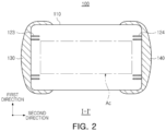
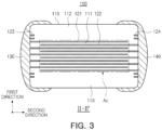
- FIG. 4 is a cross-sectional view taken along line III-III' of FIG. 1 .
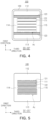
- FIGS. 8A and 8B are plan views illustrating a structure of an internal electrode according to an exemplary embodiment.
- a multilayer electronic component 100 according to an exemplary embodiment in the present disclosure will be described in detail with reference to FIGS. 1 to 5 and FIGS. 8 and 9 .
- a multilayer ceramic capacitor (MLCC) is described as an example of a multilayer electronic component, but the present disclosure is not limited thereto and may be applied to various multilayer electronic components using ceramic materials, such as inductors, piezoelectric elements, varistors, or thermistors.
- the body 110 may include a plurality of dielectric layers 111, a first internal electrode 121, a second internal electrode 122, and reinforcing patterns 123 and 124.
- the body 110 may have a hexahedral shape or a similar shape. Due to the shrinkage of ceramic powder included in the body 110 during a sintering process, the body 110 may not have a perfectly straight hexahedral shape but may have a substantially hexahedral shape.
- the body 110 may include the first and second surfaces 1 and 2 opposing each other in the first direction, the third and fourth surfaces 3 and 4 connected to the first and second surfaces 1 and 2 and opposing each other in the second direction, and the fifth and sixth surfaces 5 and 6 connected to the first and second surfaces 1 and 2, connected to the third and fourth surfaces 3 and 4, and opposing each other in the third direction.
- a step difference occurs due to the thickness of the internal electrodes 121 and 122 and the corner connecting the first surface and the third to fifth surfaces and/or the corner connecting the second surface and the third to fifth surfaces may have a shape contracted toward the center of the body 110 in the first direction when viewed from the first surface or the second surface.
- the corner connecting the first surface 1 and the third to sixth surfaces 3, 4, 5, and 6 and/or the corner connecting the second surface 2 and the third to sixth surfaces 3, 4, 5, and 6 may have a shape contracted toward the center of the body 110 in the first direction when viewed from the first surface or the second surface.
- the corner connecting the first surface and the third to sixth surfaces and/or the corner connecting the second surface and the third to sixth surfaces may have a round shape by performing a separate process to round the corner connecting each surface of the body 110.
- the portion connecting the first surface and the fifth and sixth surfaces and the portion connecting the second surface and the fifth and sixth surfaces may not have a contracted form.
- the plurality of dielectric layers 111 forming the body 110 are in a sintered state, and adjacent dielectric layers 111 may be integrated such that boundaries therebetween may not be readily apparent without using a scanning electron microscope (SEM).
- SEM scanning electron microscope
- the number of stacked dielectric layers is not particularly limited and may be determined in consideration of the size of the multilayer electronic component.
- the body may be formed by stacking 400 or more dielectric layers.
- the dielectric layer 111 may be formed by preparing a ceramic slurry including ceramic powder, an organic solvent, and a binder, applying and drying the slurry on a carrier film to prepare a ceramic green sheet, and then sintering the ceramic green sheet.
- the ceramic powder is not particularly limited as long as it may obtain sufficient capacitance, but, for example, a barium titanate-based (BaTiO 3 ) powder may be used as the ceramic powder.
- the ceramic powder may be one or more of BaTiO 3 , (Ba 1-x Ca x )TiO 3 (0 ⁇ x ⁇ 1), Ba(Ti 1-y Ca y )O 3 (0 ⁇ y ⁇ 1), (Ba 1-x Ca x ) (Ti 1-y Zr y )O 3 (0 ⁇ x ⁇ 1, 0 ⁇ y ⁇ 1) and Ba(Ti 1-y Zr y )O 3 (0 ⁇ y ⁇ 1).
- an average thickness td of the dielectric layers 111 is not particularly limited and may be arbitrarily set according to desired characteristics or purposes.
- the average thickness of the dielectric layers 111 may be 300 nm or more and 10 um or less.
- an average thickness of at least one of the plurality of dielectric layers 111 may be 300 nm or more and 10 um or less.
- the average thickness of the dielectric layer 111 may refer to an average size of the dielectric layer 111 in the first direction disposed between the internal electrodes 121 and 122.
- the average thickness of the dielectric layer 111 may be measured by scanning a cross-section of the body 110 with a scanning electron microscope (SEM) at 10,000x magnification in the first and second directions. More specifically, thicknesses at a plurality of points of one dielectric layer 111, for example, 30 equally spaced points in the second direction, may be measured and an average value thereof may be measured. The 30 equally spaced points may be designated in the capacitance formation portion Ac described below.
- the average value measurement is extended to 10 dielectric layers 111 and average values thereof are measured, the average thickness of the dielectric layer 111 may be further generalized.
- the internal electrodes 121 and 122 may be alternately arranged with the dielectric layer 111 in the first direction.
- the internal electrodes 121 and 122 may include first and second internal electrodes 121 and 122.
- the first and second internal electrodes 121 and 122 may be alternately disposed to face each other with the dielectric layer 111 constituting the body 110 interposed therebetween and may be respectively connected to the third and fourth surfaces 3 and 4 of the body 110.
- one end of the first internal electrode 121 may be connected to the third surface 3, and one end of the second internal electrode 122 may be connected to the fourth surface 4. That is, in an exemplary embodiment, the internal electrodes 121 and 122 may contact the third surface 3 or the fourth surface 4.
- the first internal electrode 121 may be connected to the third surface 3 and spaced from the fourth surface 4, and the second internal electrode 122 may be connected to the fourth surface 4 and spaced from the third surface 3. Accordingly, the first internal electrode 121 may not be connected to the second external electrode 140 and may be connected to the first external electrode 130, and the second internal electrode 122 may not be connected to the first external electrode 130 and may be connected to the second external electrode 140.
- a material for forming the internal electrodes 121 and 122 is not particularly limited, and a material having excellent electrical conductivity may be used.
- the internal electrodes 121 and 122 may include at least one of nickel (Ni), copper (Cu), palladium (Pd), silver (Ag), gold (Au), platinum (Pt), tin (Sn), tungsten (W), titanium (Ti), or alloys thereof.
- the internal electrodes 121 and 122 may be formed by printing a conductive paste for internal electrodes including at least one of nickel (Ni), copper (Cu), palladium (Pd), silver (Ag), gold (Au), platinum (Pt), tin (Sn), tungsten (W), titanium (Ti), or alloys thereof on a ceramic green sheet.
- a printing method of the conductive paste for internal electrodes may be a screen printing method or a gravure printing method, but the present disclosure is not limited thereto.
- the average thickness of the internal electrodes 121 and 122 is not particularly limited and may be arbitrarily set according to desired characteristics or purposes.
- the average thickness of the internal electrodes 121 and 122 may be 300 nm or more and 10 um or less.
- the average thickness of at least one of the plurality of internal electrodes 121 and 122 may be 300 nm or more and 10 um or less.
- the average thickness of the internal electrodes 121 and 122 is obtained as follows. In an image of a cross-section of the body 110 in length and thickness directions (L-T) taken at the center of the body 110 in the width direction scanned with a scanning electron microscope, a total of five internal electrode layers including two upper layers and two lower layers based on one internal electrode layer at a point at which a central line of the body in the length direction and a central line of the body in the thickness direction meet are extracted among the internal electrode layers, five points including two left points and two right points based on one reference point are then determined at equal intervals based on the point at which the central line of the body in the length direction and the central line of the body in the thickness direction meet, and thereafter, thicknesses at the respective points are measured and averaged.
- the body 110 may include a capacitance formation portion Ac, which is a region in which the first and second internal electrodes 121 and 122 overlap in the first direction.
- the capacitance formation portion Ac is a portion that contributes to formation of capacitance of the capacitor and may be formed by repeatedly stacking a plurality of first and second internal electrodes 121 and 122 with the dielectric layer 111 interposed therebetween.
- a region between a cross-section of the capacitance formation portion Ac in the second direction and a surface of the body 110 facing in the second direction may be referred to as a length-margin portion.
- the length-margin portion may be a region including one of the internal electrodes 121 and 122.
- cover regions 112 and 113 may be disposed on one surface and the other surface of the capacitance formation portion Ac in the first direction.
- the cover portions 112 and 113 may be formed by stacking a single dielectric layer or two or more dielectric layers in the thickness direction on upper and lower surfaces of the capacitance formation portion Ac and may basically serve to prevent damage to the internal electrodes due to physical or chemical stress.
- the cover portions 112 and 113 does not include an internal electrode and may include the same material as the dielectric layer 111.
- the cover portions 112 and 113 may include a ceramic material, for example, a barium titanate (BaTiO 3 )-based ceramic material.
- margin portions 114 and 115 may be disposed on one side and the other side of the third direction of the capacitance formation portion Ac.
- the margin portions 114 and 115 may include a first margin portion 114 disposed on the fifth surface 5 of the body 110 and a second margin portion 115 disposed on the sixth surface 6. That is, the margin portions 114 and 115 may be disposed on both end surfaces of the ceramic body 110 in the width direction.
- the margin portions 114 and 115 may refer to a region between both ends of the first and second internal electrodes 121 and 122 and a boundary surface of the body 110 in a cross-section of the body 110 taken in the width-thickness (W-T) direction.
- the margin portions 114 and 115 may basically play a role in preventing damage to the internal electrodes due to physical or chemical stress.
- the margin portions 114 and 115 may be formed by applying a conductive paste to form internal electrodes, except for the region in which the margin portion is to be formed on the ceramic green sheet.
- the average width of the margin portions 114 and 115 may refer to an average size in the third direction of a region in which the internal electrode is spaced apart from the fifth surface and an average size in the third direction of a region in which the internal electrode is spaced apart from the sixth surface and may be an average value of the sizes in the third direction of the margin portions 114 and 115 measured at five equally spaced points on the side surface of the capacitance formation portion Ac.
- the average size in the third direction of the region in which the internal electrodes 121 and 122 are spaced apart from the fifth and sixth surfaces may be 15 um or less, respectively.
- reinforcing patterns 123 and 124 may be disposed on one surface and the other surface of the capacitance formation portion Ac in the first direction.
- the reinforcing patterns 123 and 124 may be formed continuously in the third direction and may be in contact with the third surface 3 and the fourth surface 4, which are surfaces facing in the second direction of the body 110, respectively.
- the reinforcing pattern 123 in contact with the third surface 3 and the reinforcing pattern 124 in contact with the fourth surface 4 may be disposed to be spaced apart from each other in the second direction.
- a material forming the reinforcing patterns 123 and 124 is not particularly limited, and a material having excellent electrical conductivity may be used.
- the reinforcing patterns 123 and 124 may include one or more of nickel (Ni), copper (Cu), palladium (Pd), silver (Ag), gold (Au), platinum (Pt), tin (Sn), tungsten (W), titanium (Ti), and alloys thereof.
- the external electrodes 130 and 140 may be disposed on the body 110. Specifically, the external electrodes 130 and 140 may be disposed on the third and fourth surfaces 3 and 4 of the body 110, respectively, and may include first and second external electrodes 130 and 140 connected to the first and second internal electrodes 121 and 122, respectively.
- the multilayer electronic component 100 has two external electrodes 130 and 140 is described, but the number or shape of the external electrodes 130 and 140 may be changed depending on the shape of the internal electrodes 121 and 122 or other purposes.
- the external electrodes 130 and 140 may be formed using any material having electrical conductivity, such as metal, and a specific material may be determined in consideration of electrical characteristics, structural stability, etc., and may further have a multilayer structure.
- the external electrodes 130 and 140 may include an electrode layer disposed on the body 110 and a plating layer formed on the electrode layer.
- the electrode layer may be a sintered electrode including a conductive metal and glass or a resin-based electrode including a conductive metal and resin.
- the electrode layer may be in the form of a sintering electrode and a resin-based electrode being sequentially formed on the body.
- the electrode layer may be formed by transferring a sheet including a conductive metal onto the body or may be formed by transferring a sheet including a conductive metal onto a sintered electrode.
- the electrode layer may be formed as a plating layer or may be a layer formed using a deposition method, such as a sputtering method or atomic layer deposition (ALD).
- a material having excellent electrical conductivity may be used as the conductive metal included in the electrode layer and is not particularly limited.
- the conductive metal may be at least one of nickel (Ni), copper (Cu), or alloys thereof.
- the plating layer plays a role in improving the mounting characteristics.
- the type of the plating layer is not particularly limited and may be a plating layer including at least one of Ni, Sn, Pd, or alloys thereof and may include a plurality of layers.
- the plating layer may be a Ni plating layer or a Sn plating layer and may be in a form in which a Ni plating layer and a Sn plating layer are sequentially formed on an electrode layer or may be in a form in which a Sn plating layer, a Ni plating layer, and a Sn plating layer are sequentially formed.
- the plating layer may include a plurality of Ni plating layers and/or a plurality of Sn plating layers.
- the plating layer may be in a form in which a Ni plating layer and a Pd plating layer are sequentially formed on an electrode layer.
- the size of the multilayer electronic component 100 may not be particularly limited. Since the present disclosure is advantageous in miniaturization and high capacitance, the present disclosure may be applied to the size of small IT products, and since high reliability is secured in various environments, the present disclosure may be applied to the size of automotive electrical products that require high reliability.
- the external electrode of the related art general multilayer electronic component may be formed to be thin at a corner portion compared to the center of the body surface.
- the thinner portion of the external electrode may become a path for external moisture penetration, so the moisture resistance reliability may be reduced.
- a step difference may occur during the stacking and compressing process.
- a step difference may occur between the capacitance formation portion in which the internal electrodes overlap and the margin portion forming the side surface of the capacitance formation portion.
- a clumping phenomenon may occur when undergoing a heat treatment process, such as sintering.
- reinforcing patterns 123 and 124 may be disposed on one surface and the other surface of the capacitance formation portion Ac in the first direction and the reinforcing patterns 123 and 124 are disposed to be in contact with the surfaces 3 and 4 facing each other in the second direction of the body 110 and are spaced apart from each other in the second direction.
- a length of the reinforcing patterns 123 and 124 at a 1/4 point (1/4w) in the second direction may be adjusted to be greater than a length of the reinforcing patterns 123 and 124 at a 1/2 point (1/2w) in the second direction
- a length of the reinforcing patterns 123 and 124 at a 3/4 point (3/4w) in the second direction may be adjusted to be greater than a length of the reinforcing patterns 123 and 124 at the 1/2 point (1/2w) in the second direction, thereby improving the moisture resistance reliability of the multilayer electronic component, alleviating a step difference, and alleviating the clumping phenomenon at the center of the internal electrodes as well.
- the reinforcing patterns 123 and 124 when the reinforcing patterns 123 and 124 are divided into four parts in the third direction from one end thereof in the third direction to the other end thereof in the third direction, a length of the reinforcing patterns 123 and 124 at a 1/4 point (1/4w) in the second direction may be adjusted to be greater than a length of the reinforcing patterns 123 and 124 at a 1/2 point (1/2w) in the second direction, and a length of the reinforcing patterns 123 and 124 at a 3/4 point (3/4w) in the second direction may be adjusted to be greater than a length of the reinforcing patterns 123 and 124 at the 1/2 point (1/2w) in the second direction, the reinforcing patterns 123 and 124 may have a shape in which the length of the reinforcing patterns 123 and 124 in the second direction may increase from the center of the reinforcing patterns 123 and 124 in the third direction toward both ends of the reinforcing patterns 123 and 124 in the third direction
- the reinforcing patterns 123 and 124 may be disposed to be in contact with the third surface 3 and the fourth surface 4, which are surfaces of the body 110 facing in the second direction, may be spaced apart from each other in the second direction, respectively, and may have a shape in which the length in the second direction gradually increases from the center in the third direction to both ends in the third direction.
- the reinforcing patterns 123 and 124 may not overlap the capacitance formation portion Ac in the first direction.
- the reinforcing patterns 123 and 124 may be formed continuously in the third direction, and the reinforcing patterns 123 and 124 may be in contact with the fifth surface 5 and the sixth surface 6, which are surfaces facing in the third direction of the body 110. Accordingly, since the thickness of the external electrodes disposed in the region adjacent to the corner of the body 110 may be formed to be sufficiently thick, the moisture resistance reliability of the multilayer electronic component 100 may be further improved.
- the maximum length of the body 110 in the second direction may be denoted as L
- the maximum length of the reinforcing patterns 123 and 124 in the second direction may be denoted as L1
- an average length of the length-margin portion in the second direction may be denoted as LM
- the length of the reinforcing patterns 123 and 124 closest to the capacitance formation portion Ac in second direction may be denoted as L2
- the minimum length of the reinforcing patterns 123 and 124 in the second direction may be denoted as L3.
- L1 ⁇ 0.22L may be satisfied. Accordingly, even when the external electrodes are formed to extend to the fifth surface 5 or the sixth surface 6, the connectivity between the external electrodes 130 and 140 and the body 110 may be improved, and since the external electrodes 130 and 140 having a sufficient thickness may be formed at the corner connecting the third surface 3 and the fifth surface 5 and the sixth surface 6 or the corner connecting the fourth surface 4 and the fifth surface 5 and the sixth surface 6, so that the moisture resistance reliability of the multilayer electronic component 100 may be further improved. Meanwhile, the reinforcing patterns 123 and 124 have a form in which the length in second direction gradually increases from the center in third direction to both ends in the third direction, and thus, L2 ⁇ L1 may be satisfied.
- L2 ⁇ 0.95LM may be satisfied. If L2 exceeds 0.95 LM and if distortion occurs during the stacking and compressing process of the internal electrodes 121 and 122 and the reinforcing patterns 123 and 124, the reinforcing patterns 123 and 124 may overlap the capacitance formation portion Ac, thereby deteriorating the reliability of the multilayer electronic component 100. Accordingly, in an exemplary embodiment, by satisfying L2 ⁇ 0.95LM, the overlapping of the reinforcing patterns 123 and 124 and the capacitance formation portion Ac in the first direction may be prevented. Meanwhile, since the reinforcing patterns 123 and 124 have a form in which the length in the second direction gradually increases from the center in the third direction to both ends in the third direction, L3 ⁇ L2 may be satisfied.
- 0.05 LM ⁇ L3 ⁇ 0.5 LM may be satisfied. If L3 is less than 0.05 LM, the size of the reinforcing patterns 123 and 124 in the second direction may become excessively small, which may result in a decrease in the connectivity between the external electrodes 130 and 140 and the body 110, and if L3 exceeds 0.5 LM, the capacitance formation portion Ac and the reinforcing patterns 123 and 124 may overlap in the first direction, making it difficult to secure the effect of alleviating a step difference. Accordingly, in an exemplary embodiment, by adjusting to satisfy 0.05 LM ⁇ L3 ⁇ 0.5 LM, the connectivity between the external electrodes 130 and 140 and the body 110 may be improved and the effect of alleviating a step difference may be secured.
- At least two of the condition satisfying L2 ⁇ L1 ⁇ 0.22L, the condition satisfying L3 ⁇ L2 ⁇ 0.95 LM, and the condition satisfying 0.05 LM ⁇ L3 ⁇ 0.5 LM may be satisfied, and accordingly, the effect of improving the connectivity between the external electrodes 130 and 140 and the body 110 and the effect of alleviating a step difference in the multilayer electronic component 100 may be further improved.
- the method of measuring the LM, L1, L2, and L3 is not particularly limited.
- each dimension is shown in the cross-section in the second direction and third direction for convenience of description, but the present disclosure is not limited thereto, and LM, L1, L2, and L3 may be measured in the cross-section in the first direction and second direction polished to a specific point of the multilayer electronic component 100 in the third direction.
- L1 may be measured as a length of the end of the exposed reinforcing patterns 123 and 124 in the second direction. Meanwhile, in a case in which a plurality of reinforcing patterns 123 and 124 are formed, an average value of values measured in two or more layers may be taken.
- L2 may be measured as a length of the end of the exposed reinforcing patterns 123 and 124 in the second direction in the cross-section in the first direction and the second direction exposing a cross-section of the capacitance formation portion Ac in the third direction by polishing the multilayer electronic component 100 in the third direction. Meanwhile, in a case in which the plurality of reinforcing patterns 123 and 124 are formed, an average value of values measured in two or more layers may be taken.
- L3 may be measured as a length of the end of the exposed reinforcing patterns 123 and 124 in the second direction in the cross-section in the first direction and the second direction after polishing the multilayer electronic component 100 to the center portion in the third direction. Meanwhile, when a plurality of reinforcing patterns 123 and 124 are formed, an average value of values measured in two or more layers may be taken.
- LM may be measured as a length in the second direction in which the second internal electrode 122 and the third surface 3 are spaced apart in the cross-section in the first direction and the second direction after polishing the multilayer electronic component 100 to the center portion in the third direction.
- LM may be a value obtained by averaging values measured at three or more points at equal intervals in the first direction.
- FIG. 6 is a cross-sectional view taken along line II-II' of FIG. 1 in a multilayer electronic component according to an exemplary embodiment.
- FIG. 7 is a cross-sectional view taken along line II-II' of FIG. 1 in a multilayer electronic component according to an exemplary embodiment.
- a capacitance formation portion of a multilayer electronic component 100' may include a first capacitance formation portion Ac1 adjacent to one surface of the body 110 in the first direction and a second capacitance formation portion Ac2 adjacent to the other surface of the body 110 in the first direction.
- the reinforcing patterns 123 and 124 may also be disposed between the first capacitance formation portion Ac1 and the second capacitance formation portion Ac2.
- a capacitance formation portion of a multilayer electronic component 100" may include a first capacitance formation portion Ac1 adjacent to one surface of the body 110 in the first direction, a second capacitance formation portion Ac2 adjacent to the other surface of the body 110 in the first direction, and a third capacitance formation portion Ac3 disposed between the first capacitance formation portion Ac1 and the second capacitance formation portion Ac2.
- the reinforcing patterns 123 and 124 may be disposed between the first capacitance formation portion Ac1 and the third capacitance formation portion Ac3 and between the third capacitance formation portion Ac3 and the second capacitance formation portion Ac2.
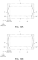
- FIGS. 10A and 10B are plan views illustrating a structure of a reinforcing pattern according to an exemplary embodiment.
- reinforcing patterns 123' and 124' may have substantially the same length in the second direction in a region beyond the cross-section of the capacitance formation portion Ac in the third direction.
- the term “substantially the same” (“about,” “approximately,” etc.) may indicate “being the same” or being within an industry-accepted tolerance, due to a process error or a measurement error recognizable by one of ordinary skill in the art provide, for the corresponding term and/or relativity between items, such as a tolerance of ⁇ 1%, ⁇ 5%, or ⁇ 10% of the actual value stated, and other suitable tolerances.
- side surfaces of the reinforcing patterns 123" and 124" according to an exemplary embodiment facing the capacitance formation portion may have a rounded shape. Accordingly, even if printing blur or clumping occurs during printing, stacking, compressing, and sintering processes, the phenomenon in which the reinforcing patterns 123" and 124" and the capacitance formation portion Ac overlap in the first direction may be effectively prevented.
- the side surfaces of the reinforcing pattern 123" and 124" facing the capacitance formation portion Ac may refer to the side surfaces of the reinforcing pattern 123" and 124" that are not in contact with the surface of the body 110.
- One of the various effects of the present disclosure is to improve the moisture resistance reliability of the multilayer electronic component by forming the reinforcing patterns on one surface and the other surface of the capacitance formation portion in the first direction and adjusting the shape thereof.
- One of the various effects of the present disclosure is to reduce a step difference of the multilayer electronic component and suppress the clumping of the central portion of the internal electrode by forming the reinforcing patterns to be spaced apart from each other in the second direction and contact the surfaces of the body facing each other in the second direction and to gradually increase in the length in the second direction toward both ends thereof in the third direction from the center portion thereof in the third direction.
- an exemplary embodiment or one example used in the present disclosure does not refer to identical examples and is provided to stress different unique features between each of the examples.
- examples provided in the following description are not excluded from being associated with features of other examples and implemented thereafter. For example, even if matters described in a specific example are not described in a different example thereto, the matters may be understood as being related to the other example, unless otherwise mentioned in descriptions thereof.
Landscapes
- Engineering & Computer Science (AREA)
- Power Engineering (AREA)
- Manufacturing & Machinery (AREA)
- Microelectronics & Electronic Packaging (AREA)
- Chemical & Material Sciences (AREA)
- Ceramic Engineering (AREA)
- Inorganic Chemistry (AREA)
- Materials Engineering (AREA)
- Fixed Capacitors And Capacitor Manufacturing Machines (AREA)
- Ceramic Capacitors (AREA)
Applications Claiming Priority (1)
| Application Number | Priority Date | Filing Date | Title |
|---|---|---|---|
| KR1020230196339A KR20250104204A (ko) | 2023-12-29 | 2023-12-29 | 적층형 전자 부품 |
Publications (2)
| Publication Number | Publication Date |
|---|---|
| EP4579698A2 true EP4579698A2 (de) | 2025-07-02 |
| EP4579698A3 EP4579698A3 (de) | 2025-11-19 |
Family
ID=93893388
Family Applications (1)
| Application Number | Title | Priority Date | Filing Date |
|---|---|---|---|
| EP24219130.2A Pending EP4579698A3 (de) | 2023-12-29 | 2024-12-11 | Mehrschichtiges elektronisches bauteil mit verstärkungsmustern oder kurzen dummy-elektroden zur vermeidung von rissen in den ecken |
Country Status (5)
| Country | Link |
|---|---|
| US (1) | US20250218689A1 (de) |
| EP (1) | EP4579698A3 (de) |
| JP (1) | JP2025105518A (de) |
| KR (1) | KR20250104204A (de) |
| CN (1) | CN120236890A (de) |
Family Cites Families (7)
| Publication number | Priority date | Publication date | Assignee | Title |
|---|---|---|---|---|
| JPH09129476A (ja) * | 1995-10-30 | 1997-05-16 | Murata Mfg Co Ltd | セラミック電子部品 |
| GB2466097B (en) * | 2008-08-18 | 2013-02-13 | Avx Corp | Ultra broadband capacitor |
| JP5672162B2 (ja) * | 2010-07-21 | 2015-02-18 | 株式会社村田製作所 | 電子部品 |
| JP2018056543A (ja) * | 2016-09-29 | 2018-04-05 | サムソン エレクトロ−メカニックス カンパニーリミテッド. | 積層型キャパシタ及びその製造方法 |
| DE112019001177T5 (de) * | 2018-03-06 | 2020-12-10 | Avx Corporation | Mehrschichtiger Keramikkondensator mit Ultrabreitbandleistungsfähigkeit |
| US11069479B2 (en) * | 2018-07-19 | 2021-07-20 | Samsung Electro-Mechanics Co., Ltd. | Multilayer capacitor |
| US20230080124A1 (en) * | 2020-02-11 | 2023-03-16 | Amotech Co., Ltd. | Broadband capacitor |
-
2023
- 2023-12-29 KR KR1020230196339A patent/KR20250104204A/ko active Pending
-
2024
- 2024-12-11 EP EP24219130.2A patent/EP4579698A3/de active Pending
- 2024-12-18 JP JP2024221378A patent/JP2025105518A/ja active Pending
- 2024-12-23 US US18/999,430 patent/US20250218689A1/en active Pending
- 2024-12-27 CN CN202411950051.0A patent/CN120236890A/zh active Pending
Also Published As
| Publication number | Publication date |
|---|---|
| KR20250104204A (ko) | 2025-07-08 |
| CN120236890A (zh) | 2025-07-01 |
| US20250218689A1 (en) | 2025-07-03 |
| EP4579698A3 (de) | 2025-11-19 |
| JP2025105518A (ja) | 2025-07-10 |
Similar Documents
| Publication | Publication Date | Title |
|---|---|---|
| US11476047B2 (en) | Multilayer electronic component | |
| KR20230117793A (ko) | 적층형 전자 부품 | |
| US20250054692A1 (en) | Multilayer electronic component | |
| JP2025105529A (ja) | 積層型電子部品 | |
| US12462980B2 (en) | Multilayer electronic component | |
| US12278056B2 (en) | Multilayer electronic component | |
| EP4579698A2 (de) | Mehrschichtiges elektronisches bauteil mit verstärkungsmustern oder kurzen dummy-elektroden zur vermeidung von rissen in den ecken | |
| US20250104922A1 (en) | Multilayer electronic component and method for manufacturing the same | |
| US20250218670A1 (en) | Multilayer electronic component | |
| US20250218685A1 (en) | Multilayer electronic component | |
| US20250218669A1 (en) | Multilayer electronic component | |
| US20250218667A1 (en) | Multilayer electronic component | |
| US12451288B2 (en) | Multilayer electronic component | |
| EP4415013B1 (de) | Mehrschichtiges keramisches elektronikbauteil mit einer interdigitalen metallzwischenschicht zwischen der inneren und der äusseren elektrode | |
| EP4578843A1 (de) | Mehrschichtiges elektronisches bauteil | |
| US20250218671A1 (en) | Multilayer electronic component | |
| US20250239407A1 (en) | Multilayer electronic component and method of manufacturing the same | |
| US20240274355A1 (en) | Multilayer electronic component | |
| US11600441B2 (en) | Multilayer electronic component | |
| US20250166923A1 (en) | Multilayer electronic component | |
| US20240212933A1 (en) | Multilayer electronic component | |
| KR20250045425A (ko) | 적층형 전자 부품 및 적층형 전자 부픔의 제조방법 | |
| KR20250063612A (ko) | 적층형 전자 부품의 제조방법 | |
| KR20240156206A (ko) | 적층형 전자 부품 | |
| CN120199616A (zh) | 多层电子组件 |
Legal Events
| Date | Code | Title | Description |
|---|---|---|---|
| PUAI | Public reference made under article 153(3) epc to a published international application that has entered the european phase |
Free format text: ORIGINAL CODE: 0009012 |
|
| STAA | Information on the status of an ep patent application or granted ep patent |
Free format text: STATUS: THE APPLICATION HAS BEEN PUBLISHED |
|
| AK | Designated contracting states |
Kind code of ref document: A2 Designated state(s): AL AT BE BG CH CY CZ DE DK EE ES FI FR GB GR HR HU IE IS IT LI LT LU LV MC ME MK MT NL NO PL PT RO RS SE SI SK SM TR |
|
| REG | Reference to a national code |
Ref country code: DE Ref legal event code: R079 Free format text: PREVIOUS MAIN CLASS: H01G0004005000 Ipc: H01G0004300000 |
|
| PUAL | Search report despatched |
Free format text: ORIGINAL CODE: 0009013 |
|
| AK | Designated contracting states |
Kind code of ref document: A3 Designated state(s): AL AT BE BG CH CY CZ DE DK EE ES FI FR GB GR HR HU IE IS IT LI LT LU LV MC ME MK MT NL NO PL PT RO RS SE SI SK SM TR |
|
| RIC1 | Information provided on ipc code assigned before grant |
Ipc: H01G 4/30 20060101AFI20251016BHEP Ipc: H01G 4/232 20060101ALI20251016BHEP Ipc: H01G 4/005 20060101ALI20251016BHEP Ipc: H01G 4/008 20060101ALI20251016BHEP Ipc: H01G 4/012 20060101ALI20251016BHEP Ipc: H01G 4/12 20060101ALN20251016BHEP |