EP4401104A2 - Mehrschichtiges elektronisches bauteil - Google Patents
Mehrschichtiges elektronisches bauteil Download PDFInfo
- Publication number
- EP4401104A2 EP4401104A2 EP23198781.9A EP23198781A EP4401104A2 EP 4401104 A2 EP4401104 A2 EP 4401104A2 EP 23198781 A EP23198781 A EP 23198781A EP 4401104 A2 EP4401104 A2 EP 4401104A2
- Authority
- EP
- European Patent Office
- Prior art keywords
- electrode layer
- disposed
- electronic component
- electrode
- additive element
- Prior art date
- Legal status (The legal status is an assumption and is not a legal conclusion. Google has not performed a legal analysis and makes no representation as to the accuracy of the status listed.)
- Pending
Links
Images


Classifications
-
- H—ELECTRICITY
- H01—ELECTRIC ELEMENTS
- H01G—CAPACITORS; CAPACITORS, RECTIFIERS, DETECTORS, SWITCHING DEVICES, LIGHT-SENSITIVE OR TEMPERATURE-SENSITIVE DEVICES OF THE ELECTROLYTIC TYPE
- H01G4/00—Fixed capacitors; Processes of their manufacture
- H01G4/002—Details
- H01G4/018—Dielectrics
- H01G4/06—Solid dielectrics
- H01G4/08—Inorganic dielectrics
- H01G4/12—Ceramic dielectrics
- H01G4/1209—Ceramic dielectrics characterised by the ceramic dielectric material
- H01G4/1218—Ceramic dielectrics characterised by the ceramic dielectric material based on titanium oxides or titanates
- H01G4/1227—Ceramic dielectrics characterised by the ceramic dielectric material based on titanium oxides or titanates based on alkaline earth titanates
-
- H—ELECTRICITY
- H01—ELECTRIC ELEMENTS
- H01G—CAPACITORS; CAPACITORS, RECTIFIERS, DETECTORS, SWITCHING DEVICES, LIGHT-SENSITIVE OR TEMPERATURE-SENSITIVE DEVICES OF THE ELECTROLYTIC TYPE
- H01G4/00—Fixed capacitors; Processes of their manufacture
- H01G4/002—Details
- H01G4/005—Electrodes
- H01G4/008—Selection of materials
-
- H—ELECTRICITY
- H01—ELECTRIC ELEMENTS
- H01G—CAPACITORS; CAPACITORS, RECTIFIERS, DETECTORS, SWITCHING DEVICES, LIGHT-SENSITIVE OR TEMPERATURE-SENSITIVE DEVICES OF THE ELECTROLYTIC TYPE
- H01G4/00—Fixed capacitors; Processes of their manufacture
- H01G4/002—Details
- H01G4/005—Electrodes
- H01G4/012—Form of non-self-supporting electrodes
-
- H—ELECTRICITY
- H01—ELECTRIC ELEMENTS
- H01G—CAPACITORS; CAPACITORS, RECTIFIERS, DETECTORS, SWITCHING DEVICES, LIGHT-SENSITIVE OR TEMPERATURE-SENSITIVE DEVICES OF THE ELECTROLYTIC TYPE
- H01G4/00—Fixed capacitors; Processes of their manufacture
- H01G4/002—Details
- H01G4/018—Dielectrics
- H01G4/06—Solid dielectrics
- H01G4/08—Inorganic dielectrics
- H01G4/12—Ceramic dielectrics
-
- H—ELECTRICITY
- H01—ELECTRIC ELEMENTS
- H01G—CAPACITORS; CAPACITORS, RECTIFIERS, DETECTORS, SWITCHING DEVICES, LIGHT-SENSITIVE OR TEMPERATURE-SENSITIVE DEVICES OF THE ELECTROLYTIC TYPE
- H01G4/00—Fixed capacitors; Processes of their manufacture
- H01G4/002—Details
- H01G4/228—Terminals
- H01G4/232—Terminals electrically connecting two or more layers of a stacked or rolled capacitor
- H01G4/2325—Terminals electrically connecting two or more layers of a stacked or rolled capacitor characterised by the material of the terminals
-
- H—ELECTRICITY
- H01—ELECTRIC ELEMENTS
- H01G—CAPACITORS; CAPACITORS, RECTIFIERS, DETECTORS, SWITCHING DEVICES, LIGHT-SENSITIVE OR TEMPERATURE-SENSITIVE DEVICES OF THE ELECTROLYTIC TYPE
- H01G4/00—Fixed capacitors; Processes of their manufacture
- H01G4/30—Stacked capacitors
-
- H—ELECTRICITY
- H01—ELECTRIC ELEMENTS
- H01G—CAPACITORS; CAPACITORS, RECTIFIERS, DETECTORS, SWITCHING DEVICES, LIGHT-SENSITIVE OR TEMPERATURE-SENSITIVE DEVICES OF THE ELECTROLYTIC TYPE
- H01G4/00—Fixed capacitors; Processes of their manufacture
- H01G4/002—Details
- H01G4/228—Terminals
- H01G4/248—Terminals the terminals embracing or surrounding the capacitive element, e.g. caps
Definitions
- the present disclosure relates to a multilayer electronic component.
- a Multilayer Ceramic Capacitor a multilayer electronic component, is a chip-type capacitor mounted on the printed circuit boards of various electronic products including video display devices such as liquid crystal displays (LCDs) and plasma display panels (PDPs), computers, smartphones, and mobile phones, to serve to charge or discharge electricity.
- video display devices such as liquid crystal displays (LCDs) and plasma display panels (PDPs)
- LCDs liquid crystal displays
- PDPs plasma display panels
- computers smartphones, and mobile phones, to serve to charge or discharge electricity.
- Multilayer ceramic capacitors may be used as components of various electronic devices due to the advantages of being small, high capacitance guaranteed, and easy to mount.
- various electronic devices such as computers and mobile devices are miniaturized and high-powered, the demand for miniaturization and high capacitance multilayer ceramic capacitors is increasing.
- the importance of increasing the capacitance per unit volume of multilayer ceramic capacitors is increasing.
- multilayer ceramic capacitors are required to have high resistance to external stress caused by deformation of a substrate or the like. If the multilayer ceramic capacitor does not have resistance to stress, moisture resistance and high-temperature reliability may deteriorate due to cracks.
- the conductive resin layer may increase equivalent series resistance (ESR) due to high resistance thereof, thereby reducing power efficiency of the multilayer ceramic capacitor or increasing heat generation, and there is a problem of a limit to thin layering.
- ESR equivalent series resistance
- An aspect of the present disclosure is to prevent cracks from occurring in the body due to external stress.
- An aspect of the present disclosure is to improve moisture resistance reliability of multilayer electronic components.
- An aspect of the present disclosure is to prevent hydrogen generated in the plating process from penetrating into the body.
- a multilayer electronic component includes a body including a dielectric layer and first and second internal electrodes alternately disposed with the dielectric layer interposed therebetween, and having a first surface and a second surface opposing each other in a first direction, a third surface and a fourth surface connected to the first and second surfaces and opposing each other in a second direction, and a fifth surface and a sixth surface connected to the first to fourth surfaces and opposing each other in a third direction; a first external electrode including a 1-1-th electrode layer disposed on the third surface, and a 1-2-th electrode layer disposed on the first and second surfaces and connected to the 1-1-th electrode layer; and a second external electrode including a 2-1-th electrode layer disposed on the fourth surface and a 2-2-th electrode layer disposed on the first and second surfaces and connected to the 2-1-th electrode layer.
- the 1-2-th electrode layer and the 2-2-th electrode layer include Cu and a first additive element having a content lower than a content of the Cu, the content of the first additive element included in the 1-2-th electrode layer is greater than the content of the first additive element included in the 1-1-th electrode layer, and the content of the first additive element included in the 2-2-th electrode layer is greater than the content of the first additive element included in the 2-1-th electrode layer, and the first additive element is at least one selected from Ag and Al.
- a multilayer electronic component includes a body including a dielectric layer and first and second internal electrodes alternately disposed with the dielectric layer interposed therebetween, and having a first surface and a second surface opposing each other in a first direction, a third surface and a fourth surface connected to the first and second surfaces and opposing each other in a second direction, and a fifth surface and a sixth surface connected to the first to fourth surfaces and opposing each other in a third direction; a first external electrode including a 1-1-th electrode layer disposed on the third surface, and a 1-2-th electrode layer disposed on the first and second surfaces and connected to the 1-1-th electrode layer; and a second external electrode including a 2-1-th electrode layer disposed on the fourth surface, and a 2-2-th electrode layer disposed on the first and second surfaces and connected to the 2-1-th electrode layer.
- the 1-1-th electrode layer and the 2-1-th electrode layer are disposed between an extension line of the first surface and an extension line of the second surface, the 1-1-th electrode layer includes a region not covered by the 1-2-th electrode layer on the third surface, the 2-1-th electrode layer includes a region not covered by the 2-2-th electrode layer on the fourth surface, and the 1-2-th electrode layer and the 2-2-th electrode layer each contain at least one of Ag and Al.
- the first direction may be defined as the thickness (T) direction
- the second direction may be defined as the length (L) direction
- the third direction may be defined as the width (W) direction.
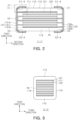
- FIG. 1 is a perspective view schematically illustrating a multilayer electronic component according to an embodiment.
- FIG. 2 is a cross-sectional view schematically illustrating a section taken along line I-I' of FIG. 1 .
- FIG. 3 is a cross-sectional view schematically illustrating a section taken along line II-II' of FIG. 1 .
- FIG. 4 is an exploded perspective view schematically illustrating an exploded body of a multilayer electronic component according to an embodiment.
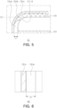
- FIG. 5 is an enlarged view of region K1 in FIG. 2 .
- FIG. 6 is an enlarged view of region K2 of FIG. 2 .
- FIG. 7 is a cross-sectional view schematically illustrating a cross-section of an external electrode of a multilayer electronic component according to an embodiment.
- a multilayer electronic component 100 may include a body 110 including a dielectric layer 111 and first and second internal electrodes 121 and 122 alternately disposed with the dielectric layer interposed therebetween, and having first and second surfaces 1 and 2 opposing each other in the first direction, third and fourth surfaces 3 and 4 connected to the first and second surfaces and opposing each other in the second direction, and fifth and sixth surfaces 5 and 6 connected to the first to fourth surfaces and opposing each other in the third direction, a first external electrode 131 including a 1-1-th electrode layer 131a disposed on the third surface, and a 1-2-th electrode layer 131b disposed on the first and second surfaces and connected to the 1-1-th electrode layer, and a second external electrode 132 including a 2-1-th electrode layer 132a disposed on the fourth surface, and a 2-2-th electrode layer 132b disposed on the first and second surfaces and connected to the 2-1-th electrode layer.
- the 1-2-th electrode layer 131b and the 2-2-th electrode layer 132b include Cu and a first additive element having a content lower than the Cu content, the content of the first additive element included in the 1-2-th electrode layer 131b is greater than the content of the first additive element included in the 1-1-th electrode layer 131a, the content of the first additive element included in the 2-2-th electrode layer 132b is greater than the content of the first additive element included in the 2-1-th electrode layer 132a, and the first additive element may be at least one selected from Ag and Al.
- the first additive element having excellent ductility is included in the 1-2-th electrode layer 131b and the 2-2-th electrode layer 132b disposed on the mounting surface, and since the content of the first additive element included in the 1-2-th electrode layer 131b and the 2-2-th electrode layer 132b is greater than that of the 1-1-th electrode layer 131a and the 2-1-th electrode layer 132a, cracks may be prevented from occurring in the body 110 due to external stress, and accordingly, moisture resistance and high-temperature reliability of multilayer electronic components may be improved.
- the body 110 may have a hexahedral shape or a shape similar thereto. Due to shrinkage of the ceramic powder included in the body 110 during the sintering process or polishing of the corners, the body 110 may not have a hexahedral shape with perfect straight lines, but may substantially have a hexahedral shape.
- the body 110 may have first and second surfaces 1 and 2 opposing each other in the first direction, third and fourth surfaces 3 and 4 connected to the first and second surfaces 1 and 2 and opposing each other in the second direction, and fifth and sixth surfaces 5 and 6 connected to the first to fourth surfaces 1, 2, 3, and 4 and opposing each other in the third direction.
- the body 110 may include a 1-3-th corner C1-3 connecting the first surface and the third surface, a 1-4 corner C1-4 connecting the first surface and the fourth surface, a 2-3-th corner C2-3 connecting the second and third surfaces, and a 2-4 corner C2-4 connecting the second and fourth surfaces.
- the body 110 may include a 1-5-th corner connecting the first surface and the fifth surface, a 1-6-th corner connecting the first surface and the sixth surface, a 2-5-th corner connecting the second surface and the fifth surface, and a 2-6-th corner connecting the second surface 2 and the sixth surface 6.
- the corner may have a round shape by rounding the corner connecting each side of the body 110 by performing a separate process.
- the first to sixth surfaces of the body 110 may be substantially flat surfaces, and non-flat areas may be viewed as corners.
- dielectric layers 111 and internal electrodes 121 and 122 may be alternately stacked.
- the plurality of dielectric layers 111 forming the body 110 are in a sintered body, and a boundary between adjacent dielectric layers 111 may be unified to the extent that it is difficult to confirm without using a scanning electron microscope (SEM).
- the dielectric layer 111 may be formed by preparing a ceramic slurry containing ceramic powder, an organic solvent and a binder, applying and drying the slurry on a carrier film to prepare a ceramic green sheet, and then sintering the ceramic green sheet.
- the ceramic powder is not particularly limited as long as sufficient capacitance may be obtained, but, for example, barium titanate-based (BaTiO 3 )-based powder may be used.
- the average thickness of the dielectric layer does not need to be particularly limited.
- the thickness of the dielectric layer 111 should be relatively thinned to increase the number of stacked layers.
- the thickness of the dielectric layer 111 becomes thinner, cracks may easily occur in the body of the multilayer electronic component due to external stress, and thus, moisture resistance and high-temperature reliability of the multilayer electronic component may be deteriorated.
- the content of the first additive element included in the 1-2-th electrode layer 131b and the 2-2-th electrode layer 132b is greater than that of the 1-1-th electrode layer 131a and the 2-1-th electrode layer 132a, thereby preventing cracks from occurring in the body 110 due to external stress.
- the average thickness of the dielectric layer 111 is 0.4 ⁇ m or less, the moisture resistance reliability and high temperature reliability of the multilayer electronic component may be secured.
- the average thickness of the dielectric layer may refer to the average thickness of the dielectric layer 111 disposed between the internal electrodes 121 and 122.
- the average thickness of the dielectric layer 111 may be measured by scanning a cross section of the body 110 in the first and second directions with a scanning electron microscope (SEM) at a magnification of 10, 000.
- SEM scanning electron microscope
- an average value may be measured by measuring the thickness at a plurality of points of one dielectric layer 111, for example, at 30 points equally spaced in the second direction. The 30 equally spaced points may be designated in a capacitance forming portion Ac to be described later.
- the average thickness of the dielectric layer 111 may be further generalized.
- the internal electrodes 121 and 122 may be alternately disposed with the dielectric layer 111.
- the first internal electrode 121 and the second internal electrode 122 which are a pair of electrodes having different polarities, may be disposed to face each other, with the dielectric layer 111 interposed therebetween.
- the plurality of first internal electrodes 121 and the plurality of second internal electrodes 122 may be electrically separated from each other by the dielectric layer 111 disposed therebetween.
- the plurality of first internal electrodes 121 may be respectively spaced apart from the fourth surface 4 and connected to the third surface 3.
- the plurality of second internal electrodes 122 may be respectively spaced apart from the third surface 3 and connected to the fourth surface 4.
- the conductive metal included in the internal electrodes 121 and 122 may be at least one of nickel (Ni), copper (Cu), palladium (Pd), silver (Ag), gold (Au), platinum (Pt), tin (Sn), tungsten (W), titanium (Ti) and alloys thereof, but the present disclosure is not limited thereto.
- the internal electrodes 121 and 122 may be formed by applying a conductive paste for internal electrodes containing a conductive metal to a predetermined thickness on a ceramic green sheet and sintering the same.
- a screen-printing method or a gravure printing method may be used as a printing method of the conductive paste for internal electrodes, but the present disclosure is not limited thereto.
- the average thickness of the internal electrode does not need to be particularly limited.
- the thickness of the internal electrodes 121 and 122 may refer to the size of the internal electrodes 121 and 122 in the first direction.
- the content of the first additive element included in the 1-2-th electrode layer 131b and the 2-2-th electrode layer 132b is greater than that of the 1-1-th electrode layer 131a and the 2-1-th electrode layer 132a, and therefore, even when the average thickness of the internal electrodes 121 and 122 is 0.4 ⁇ m or less, the moisture resistance and high temperature reliability of the multilayer electronic component may be secured.
- the average thickness of the internal electrodes may be measured by scanning a cross section of the body 110 in the first and second directions with a scanning electron microscope (SEM) at a magnification of 10,000.
- the average value may be measured by measuring the thicknesses at a plurality of points of one internal electrode 121 or 122, for example, at 30 points equally spaced in the second direction. The 30 equally spaced points may be designated in a capacitance forming portion Ac to be described later.
- the average thickness of the internal electrodes 121 and 122 may be further generalized.
- the body 110 may include the capacitance forming portion Ac disposed inside the body 110 and including a plurality of first internal electrodes 121 and a plurality of second internal electrodes 122 disposed to face each other with the dielectric layer 111 interposed therebetween, to form the capacitance, and a first cover portion 112 and a second cover portion 113 disposed on both end surfaces of the capacitance forming portion Ac facing each other in the first direction.
- the cover portions 112 and 113 may basically serve to prevent damage to the internal electrodes due to physical or chemical stress.
- the cover portions 112 and 113 may have the same configuration as the dielectric layer 111 except that they do not include internal electrodes.
- the average thickness of the cover portion does not need to be particularly limited. However, the average thickness of the cover portion may be 20 um or less for miniaturization and high capacitance of the multilayer electronic component. As described above, even when the average thickness of the cover portion is 20 ⁇ m or less, since the content of the first additive element included in the 1-2-th electrode layer 131b and the 2-2-th electrode layer 132b is greater than that of the 1-1-th electrode layer 131a and the 2-1-th electrode layer 132a, reliability of the multilayer electronic component 100 may be secured.
- the average thickness of the cover portion refers to the average thickness of each of the first cover portion 112 and the second cover portion 113.
- the average thickness of the cover portions 112 and 113 may refer to the average size of the cover portions 112 and 113 in the first direction, and may be an average value of sizes in the first direction measured at five equally spaced points in the cross section of the body 110 in the first and second directions.
- the body 110 may include margin portions 114 and 115 disposed on both end surfaces of the capacitance forming portion Ac, facing each other in the third direction.
- the margin portions 114 and 115 may refer to regions between both ends of the internal electrodes 121 and 122 and the boundary surface of the body 110 in the cross-section of the body 110 cut in the first and third directions.
- the margin portion may include a first margin portion 114 disposed on the fifth surface 5 of the body 110 and a second margin portion 115 disposed on the sixth surface 6 of the body 110.
- the margin portions 114 and 115 may include the same material as the dielectric layer 111 except that the internal electrodes 121 and 122 are not included.
- the margin portions 114 and 115 may basically serve to prevent damage to the internal electrodes 121 and 122 due to physical or chemical stress.
- the margin portions 114 and 115 may be formed by coating and sintering a conductive paste for internal electrodes on the ceramic green sheet, except where the margin portion is to be formed. Alternatively, to suppress the step difference caused by the internal electrodes 121 and 122, the margin portions 114 and 115 may also be formed by stacking a single dielectric layer or two or more dielectric layers on both end faces of the capacitance forming portion Ac, facing each other in the third direction.
- the average thickness of the margin portions 114 and 115 does not need to be particularly limited. However, the average thickness of the margin portions 114 and 115 may be 20 um or less for miniaturization and high capacitance of the multilayer electronic component. As described above, even when the average thickness of the margin portions 114 and 115 is 20 ⁇ m or less, the content of the first additive element included in the 1-2-th electrode layer 131b and the 2-2-th electrode layer 132b is greater than that of the 1-1-th electrode layer 131a and the 2-1-th electrode layer 132a. Therefore, moisture resistance and high temperature reliability of the multilayer electronic component 100 may be secured.
- the average thickness of the margin portions 114 and 115 refers to the average thickness of each of the first margin portion 114 and the second margin portion 115.
- the average thickness of the margin portions 114 and 115 may refer to the average size of the margin portions 114 and 115 in the third direction, and may be an average value of sizes in the third direction measured at five equally spaced points in the cross section of the body 110 in the first and third directions.
- the external electrodes 131 and 132 may be disposed on the third and fourth surfaces 3 and 4 of the body 110, and may include first external electrodes 131 and second external electrodes 132 connected to the plurality of first internal electrodes 121 and the plurality of second internal electrodes 122 respectively.
- the first external electrode 131 may include a 1-1-th electrode layer 131a disposed on the third surface, a 1-2-th electrode layer 131b disposed on the first and second surfaces and connected to the 1-1-th electrode layer, and a 1-3-th electrode layer 131c disposed on the 1-1-th electrode layer and the 1-2-th electrode layer.
- the second external electrode 132 may include a 2-1-th electrode layer 132a disposed on the fourth surface, a 2-2-th electrode layer 132b disposed on the first and second surfaces and connected to the 2-1-th electrode layer, and a 2-3-th electrode layer 132c disposed on the 2-1-th electrode layer and the 2-2-th electrode layer.
- each of the 1-1-th electrode layer 131a, the 1-2-th electrode layer 131b, the 2-1-th electrode layer 132a, and the 2-2-th electrode layer 132b may include metal and glass.
- the glass may include at least one oxide among, for example, Ba, Ca, Zn, Al, B, and Si, but the present disclosure is not limited thereto.
- the glass included in the 1-1-th electrode layer 131a and the 1-2-th electrode layer 131b may serve to prevent moisture from penetrating into the body 110.
- the glass included in the 1-2-th electrode layer 131b and the 2-2-th electrode layer 132b may serve to improve bonding strength with the first and second surfaces 1 and 2 of the body 110.
- the area fraction of the glass included in the 1-1-th electrode layer 131a may be greater than the area fraction of the glass included in the 1-2-th electrode layer 131b.
- the area fraction of the glass included in the 2-1-th electrode layer 132a may be greater than the area fraction of the glass included in the 2-2-th electrode layer 132b. Therefore, external moisture may be prevented from permeating into the internal electrodes 121 and 122 through the third and fourth surfaces, thereby improving moisture resistance reliability of the multilayer electronic component.
- the 1-2-th electrode layer 131b and the 2-2-th electrode layer 132b having a low area fraction of glass may be peeled off from the body 110, thereby preventing cracks from occurring in the body 110.
- the area fraction of the glass included in the 1-1-th electrode layer 131a, the 1-2-th electrode layer 131b, the 2-1-th electrode layer 132b, and the 2-2-th electrode layer 132b may refer to an area ratio of the region where the glass is disposed with respect to the total area of the region where the metal is disposed and the region where the glass is disposed.
- the area fraction may be measured, for example, by analyzing images of the first and second direction cross sections of the first and second external electrodes 131 and 132 cut at the third direction center of the body 110, taken with a scanning electron microscope (SEM).
- the area where the metal is disposed and the area where the glass is disposed may have different colors or shades, and therefore, the area fraction of glass included in the 1-1-th electrode layer 131a, the 1-2-th electrode layer 131b, the 2-1-th electrode layer 132b, and the 2-2-th electrode layer 132b may be measured.
- the region where the metal is disposed and the region where the glass is disposed may be distinguished from each other by analyzing components of images taken with the scanning electron microscope (SEM) using energy dispersive spectroscopy (EDS).
- SEM scanning electron microscope
- EDS energy dispersive spectroscopy
- the 1-2-th electrode layer 131b and the 2-2-th electrode layer 132c may also be disposed on the fifth and sixth surfaces, and any one of the first surface, the second surface, the fifth surface, and the sixth surface may be a mounting surface on which the multilayer electronic component 100 is mounted on a board.
- the 1-2-th electrode layer 131b and the 2-2-th electrode layer 132c may include Cu and a first additive element in an amount smaller than the amount of Cu, and the first additive element may be at least one selected from Ag and Al.
- Cu and the first additive element are typical metal elements with excellent ductility.
- the 1-2-th electrode layer 131b and the 2-2-th electrode layer 132b disposed on the mounting surface include Cu and the first additive element having excellent ductility, thereby preventing cracks from occurring in the body 110 due to external stress caused by deformation of the substrate or the like.
- the first additive element is superior in ductility to Cu, but if Ag is excessively added to the 1-2-th electrode layer 131b and the 2-2-th electrode layer 132b, sintering temperatures of the external electrodes 131 and 132 may be excessively low. Also, if Al is excessively added to the 1-2-th electrode layer 131b and the 2-2-th electrode layer 132b, the sintering temperature of the external electrodes 131 and 132 may become excessively high. Therefore, it may be preferable that the 1-2-th electrode layer 131b and the 2-2-th electrode layer 132b contain the first additive element in an amount smaller than the content of Cu.
- the amount of Ag may be 8 moles or more and less than 50 moles based on 100 moles of the total content of Cu and Ag. If the content of Ag is less than 8 moles, phase separation of Ag may occur during the sintering process, and if the content of Ag is more than 50 moles, the sintering temperature may be excessively low.
- the Al content when the first additive element is Al, the Al content may be 5.65 moles or more and less than 50 moles based on 100 moles of the total content of Cu and Al. If the Al content is less than 5.65 mol, a stable phase between Cu and Al may not be formed, and in the case of 50 moles or more, the sintering temperature may be excessively high.
- the content of the first additive element included in the 1-2-th electrode layer 131b is greater than the content of the first additive element included in the 1-1-th electrode layer 131a, and the content of the first additive element included in the 2-2-th electrode layer 132b may be greater than the content of the first additive element included in the 2-1-th electrode layer 132a.
- the 1-2-th electrode layer 131b and the 2-2-th electrode layer 132b are disposed on the mounting surface, to prevent cracks from occurring in the body 110 due to external stress caused by deformation of the substrate, a relatively high content of the first additive element may be included.
- the 1-1-th electrode layer 131a and the 2-1-th electrode layer 132a serve to connect the internal electrodes 121 and 122 and the external electrodes 131 and 132, it is enough to include a relatively low content of the first additive element, and accordingly, the 1-1-th electrode layer 131a and the 2-1-th electrode layer 132a may not include the first additive element, but the present disclosure is not limited thereto.
- the content of the first additive element and the content of Cu included in the 1-2-th electrode layer 131b and the 2-2-th electrode layer 132b, and the content of the first additive element included in the 1-1-th electrode layer 131a and the 2-1-th electrode layer 132a may be measured by obtaining images of cross sections in the first and second directions of the first and second external electrodes 131 and 132 cut at the center of the body 110 in the third direction with a scanning electron microscope (SEM), and then by component analysis of the images by energy dispersive spectroscopy (EDS) .
- SEM scanning electron microscope
- EDS energy dispersive spectroscopy
- the Cu content may refer to an atomic percentage (at%) measured by energy dispersive spectroscopy (EDS), and the content of the first additive element may refer to the total atomic percentage (at%) of the atomic percentage of Ag and the atomic percentage of Al.
- EDS energy dispersive spectroscopy
- the content of Cu included in the 1-2-th electrode layer 131b and the 2-2-th electrode layer 132b, and the content of the first additive element included in the 1-1-th electrode layer 131a, the 1-2-th electrode layer 131b, the 2-1-th electrode layer 132a and the 2-2-th electrode layer 132b may be measured in an area other than the glass.
- the content of the first additive element included in the 1-1-th electrode layer 131a may be measured in the area where the 1-1-th metal 131a1 is disposed, excluding the area where the 1-1-th glass 131a2 is disposed.
- the content of the first additive element included in the 1-1-th electrode layer 131a may be the content of the first additive element measured at an arbitrary point in the region where the 1-1-th metal 131a1 is disposed, but the present disclosure is not limited thereto, and the content of the first additive element included in the 1-1-th electrode layer 131a may also refer to the average value of the content of the first additive element measured at any 10 points (D1, D2, D3, D4,..) of the 1-1-th metal 131a1.
- the content of Cu and the content of the first additive element included in the 1-2-th electrode layers 131b may be measured in an area where the 1-2-th metal 131b1 is disposed, excluding the area where the 1-2-th glass 131b2 is disposed.
- the content of Cu and the content of the first additive element included in the 1-2-th electrode layers 131b may be the content of Cu and the content of the first additive element measured at any one point in the region where the 1-2-th metal 131b1 is disposed, but the present disclosure is not limited thereto.
- the content of Cu and the content of the first additive element included in the 1-2-th electrode layers 131b may refer to the average value of the content of Cu and the average value of the content of the first additive element measured at any 10 points (D1, D2, D3, D4,..) of the region where the 1-2-th metal 131b1 is disposed.
- the first external electrode 131 may be in a symmetrical relationship with the second external electrode 132 in the second direction, the above description may be equally applied to the 2-1-th electrode layer 132a and the 2-2-th electrode layer 132b of the second external electrode 132.
- the content of the first additive element and the content of Cu included in the 1-2-th electrode layer 131b and the 2-2-th electrode layer 132b, and the content of the first additive element included in the 1-1-th electrode layer 131a and the 2-1-th electrode layer 132a may be measured in the remaining metal area after the glass is selectively etched and removed.
- the 1-1-th electrode layer 131a and the 2-1-th electrode layer 132a serve to connect the internal electrodes 121 and 122 and the external electrodes 131 and 132
- Cu having excellent connectivity with the internal electrodes 121 and 122 may be included, and in more detail, a metal containing Cu as a main component may be included.
- the main component refers to a component having the highest atomic percentage (at%).
- the 1-1-th electrode layer 131a and the 2-1-th electrode layer 132a further include a second additive element
- the second additive element may be at least one selected from Ni, Sn, Si, P, S, Cl, Zn, Ga, Ge, Se, Br, Nb, In, Sb, Te, I, Hf, Ta, W, Pt, Au, Pb and Bi.
- the second additive element may serve to lower the stabilization energy of hydrogen in a metal containing Cu as a main component, thereby preventing hydrogen generated during the plating process from penetrating into the body 110.
- the 1-1-th electrode layer 131a and the 2-1-th electrode layer 132a may be disposed between the extension line E1 of the first surface and the extension line E2 of the second surface. Accordingly, the capacitance per unit volume may be improved by reducing the size of the multilayer electronic component in the first direction.
- the extension line of each surface may refer to a line extended based on the flat part of each surface.
- the 1-1-th electrode layer 131a includes a region not covered by the 1-2-th electrode layer 131b on the third surface
- the 2-1-th electrode layer 132a may include a region not covered by the 2-2-th electrode layer 132b on the fourth surface.
- the boundary between the 1-1-th electrode layer 131a and the 1-2-th electrode layer 131b may be distinguished from mapping images of the first and second additive elements obtained by analyzing the cross section in the first and second directions of the first external electrode 131 cut from the center of the body 110 in the third direction with SEM-EDS.
- the boundary between the 1-1-th electrode layer 131a and the 1-2-th electrode layer 131b may be a point where the distribution of the first and second additive elements rapidly changes.
- the boundary between the 2-1-th electrode layer 132a and the 2-2-th electrode layer 132b may be a point where the distribution of the first and second additive elements rapidly changes in the mapping images of the first and second additive elements obtained by analyzing the cross section in the first and second directions of the second external electrode 131 cut from the center of the body 110 in the third direction by SEM-EDS.
- the 1-1-th electrode layer 131a and the 2-1-th electrode layer 132a may be formed, for example, by applying a first conductive paste containing Cu powder and glass to the third and fourth surfaces and then sintering the same.
- the first conductive paste may include the first additive element powder and/or the second additive element powder.
- the 1-2-th electrode layer 131b and the 2-2-th electrode layer 132b may be formed by applying a second conductive paste containing Cu powder and a first additive element powder having a content lower than the content of the Cu powder on the first, second, fifth, and sixth surfaces, and then sintering the paste.
- the 1-3-th electrode layer 131c and the 2-3-th electrode layer 132c may improve mounting characteristics.
- the types of the 1-3-th electrode layer and the 2-3-th electrode layer are not particularly limited, and may be a plating layer including Ni, Sn, Pd, and/or alloys including the same, and may be formed of a plurality of layers.
- the 1-3-th electrode layer 131c and the 2-3-th electrode layer 132c may be, for example, a Ni plating layer or a Sn plating layer, and may have a form in which the Ni plating layer and the Sn plating layer are sequentially formed.
- the 1-3-th electrode layer 131c and the 2-3-th electrode layer 132c may include a plurality of Ni plating layers and/or a plurality of Sn plating layers.
- the multilayer electronic component according to an embodiment may have the same configuration as the above-described multilayer electronic component according to the embodiment. Therefore, description overlapping with the above-described embodiment will be omitted.
- a multilayer electronic component 100 may include a body 110 including a dielectric layer 111 and first and second internal electrodes 121 and 122 alternately disposed with the dielectric layer interposed therebetween, and having first and second surfaces 1 and 2 opposing each other in the first direction, third and fourth surfaces 3 and 4 connected to the first and second surfaces and opposing each other in the second direction, and fifth and sixth surfaces 5 and 6 connected to the first to fourth surfaces and opposing each other in the third direction, a first external electrode 131 including a 1-1-th electrode layer 131a disposed on the third surface, and a 1-2-th electrode layer 131b disposed on the first and second surfaces and connected to the 1-1-th electrode layer, and a second external electrode 132 including a 2-1-th electrode layer 132a disposed on the fourth surface, and a 2-2-th electrode layer 132b disposed on the first and second surfaces and connected to the 2-1-th electrode layer.
- the 1-1-th electrode layer 131a and the 2-1-th electrode layer 132a are disposed between the extension line E1 of the first surface and the extension line E2 of the second surface, the 1-1-th electrode layer 131a includes a region not covered by the 1-2-th electrode layer 131b on the third surface, the 2-1-th electrode layer 132a includes a region not covered by the 2-2-th electrode layer 132b on the fourth surface, and each of the 1-2-th electrode layer 131b and the 2-2-th electrode layer 132b may include at least one of Ag and Al.
- the 1-1-th electrode layer 131a and the 2-1-th electrode layer 132a are disposed between the extension line E1 of the first surface and the extension line E2 of the second surface, and thus, capacitance per unit volume may be improved by reducing the size of the multilayer electronic component in the first direction.
- the extension line of each surface may refer to a line extended based on the flat part of each surface.
- the 1-1-th electrode layer 131a includes a region not covered by the 1-2-th electrode layer 131b on the third surface
- the 2-1-th electrode layer 132a includes a region not covered by the 2-2-th electrode layer 132b on the fourth surface, thereby reducing the thickness of the first external electrode 131 disposed on the third surface and reducing the thickness of the second external electrode 132 disposed on the fourth surface.
- the capacitance per unit volume may be improved by reducing the size of the multilayer electronic component 100 in the second direction.
- the 1-2-th electrode layer 131b and the 2-2-th electrode layer 132b disposed on the mounting surface include at least one of Ag and Al having superior ductility than Cu, thereby preventing cracks from occurring in the body 110 due to external stress caused by deformation of the substrate.
- a multilayer electronic component having excellent moisture resistance and high temperature reliability may be provided.
- cracks may be prevented from occurring in the body due to external stress.
- Moisture resistance reliability of multilayer electronic components may be improved.
- Hydrogen generated in the plating process may be prevented from penetrating into the body.
- first and second are used to distinguish one component from another, and do not limit the order and/or importance of the components.
- a first element may be named a second element, and similarly, a second element may be named a first element.
Landscapes
- Engineering & Computer Science (AREA)
- Power Engineering (AREA)
- Manufacturing & Machinery (AREA)
- Microelectronics & Electronic Packaging (AREA)
- Chemical & Material Sciences (AREA)
- Ceramic Engineering (AREA)
- Inorganic Chemistry (AREA)
- Materials Engineering (AREA)
- Fixed Capacitors And Capacitor Manufacturing Machines (AREA)
- Ceramic Capacitors (AREA)
Applications Claiming Priority (1)
| Application Number | Priority Date | Filing Date | Title |
|---|---|---|---|
| KR1020220158854A KR20240076921A (ko) | 2022-11-24 | 2022-11-24 | 적층형 전자 부품 |
Publications (2)
| Publication Number | Publication Date |
|---|---|
| EP4401104A2 true EP4401104A2 (de) | 2024-07-17 |
| EP4401104A3 EP4401104A3 (de) | 2024-11-27 |
Family
ID=88146773
Family Applications (1)
| Application Number | Title | Priority Date | Filing Date |
|---|---|---|---|
| EP23198781.9A Pending EP4401104A3 (de) | 2022-11-24 | 2023-09-21 | Mehrschichtiges elektronisches bauteil |
Country Status (5)
| Country | Link |
|---|---|
| US (1) | US12462980B2 (de) |
| EP (1) | EP4401104A3 (de) |
| JP (1) | JP2024076344A (de) |
| KR (1) | KR20240076921A (de) |
| CN (1) | CN118073091A (de) |
Families Citing this family (1)
| Publication number | Priority date | Publication date | Assignee | Title |
|---|---|---|---|---|
| KR20240093028A (ko) * | 2022-12-15 | 2024-06-24 | 삼성전기주식회사 | 적층형 전자 부품 |
Family Cites Families (12)
| Publication number | Priority date | Publication date | Assignee | Title |
|---|---|---|---|---|
| JPH0817137B2 (ja) * | 1988-11-30 | 1996-02-21 | 太陽誘電株式会社 | 積層磁器コンデンサ |
| JP2001307947A (ja) | 2000-04-25 | 2001-11-02 | Tdk Corp | 積層チップ部品及びその製造方法 |
| JP5289794B2 (ja) * | 2007-03-28 | 2013-09-11 | 株式会社村田製作所 | 積層型電子部品およびその製造方法 |
| JP5282634B2 (ja) * | 2008-06-25 | 2013-09-04 | 株式会社村田製作所 | 積層セラミック電子部品およびその製造方法 |
| JP2010118499A (ja) * | 2008-11-13 | 2010-05-27 | Murata Mfg Co Ltd | 積層セラミック電子部品 |
| KR101641574B1 (ko) * | 2014-02-03 | 2016-07-22 | 삼성전기주식회사 | 기판 내장용 적층 세라믹 전자부품, 그 제조방법 및 적층 세라믹 전자부품 내장형 인쇄회로기판 |
| JP6020502B2 (ja) * | 2014-03-31 | 2016-11-02 | 株式会社村田製作所 | 積層セラミック電子部品 |
| US10446320B2 (en) * | 2016-04-15 | 2019-10-15 | Samsung Electro-Mechanics Co., Ltd. | Multilayer capacitor having external electrode including conductive resin layer |
| JP2018073900A (ja) * | 2016-10-26 | 2018-05-10 | 株式会社村田製作所 | 積層セラミックコンデンサ |
| JP2021100021A (ja) | 2019-12-20 | 2021-07-01 | 太陽誘電株式会社 | 積層セラミック電子部品 |
| JP7396191B2 (ja) | 2020-05-01 | 2023-12-12 | 株式会社村田製作所 | セラミック電子部品およびセラミック電子部品の製造方法 |
| JP7528763B2 (ja) * | 2020-12-11 | 2024-08-06 | 株式会社村田製作所 | 積層セラミック電子部品および樹脂電極用導電性ペースト |
-
2022
- 2022-11-24 KR KR1020220158854A patent/KR20240076921A/ko active Pending
-
2023
- 2023-09-21 EP EP23198781.9A patent/EP4401104A3/de active Pending
- 2023-09-28 JP JP2023167849A patent/JP2024076344A/ja active Pending
- 2023-09-29 US US18/375,311 patent/US12462980B2/en active Active
- 2023-11-16 CN CN202311540476.XA patent/CN118073091A/zh active Pending
Also Published As
| Publication number | Publication date |
|---|---|
| EP4401104A3 (de) | 2024-11-27 |
| US12462980B2 (en) | 2025-11-04 |
| US20240177933A1 (en) | 2024-05-30 |
| CN118073091A (zh) | 2024-05-24 |
| KR20240076921A (ko) | 2024-05-31 |
| JP2024076344A (ja) | 2024-06-05 |
Similar Documents
| Publication | Publication Date | Title |
|---|---|---|
| CN112309718B (zh) | 多层电子组件 | |
| US20240177934A1 (en) | Multilayer electronic component | |
| EP4401104A2 (de) | Mehrschichtiges elektronisches bauteil | |
| EP4542598A1 (de) | Mehrschichtiges elektronisches bauteil | |
| US12278056B2 (en) | Multilayer electronic component | |
| US12176153B2 (en) | Multilayer electronic component | |
| US12374496B2 (en) | Multilayer electronic component | |
| US12374497B2 (en) | Multilayer electronic component with improved reliability | |
| JP2024132785A (ja) | 積層型電子部品 | |
| EP4539068A2 (de) | Keramischer vielschichtkondensator mit mehrschichtigen aussenelektroden auf der basis von silber, kupfer als hauptbestandteil und verschiedenen gläsern | |
| EP4415013B1 (de) | Mehrschichtiges keramisches elektronikbauteil mit einer interdigitalen metallzwischenschicht zwischen der inneren und der äusseren elektrode | |
| EP4415012A1 (de) | Mehrschichtiges elektronisches bauteil | |
| EP4560668A1 (de) | Mehrschichtiges elektronisches bauteil | |
| US20250201480A1 (en) | Multilayer electronic component | |
| EP4535385A1 (de) | Mehrschichtiges elektronisches bauteil | |
| US12340944B2 (en) | Multilayer electronic component | |
| US20250218689A1 (en) | Multilayer electronic component | |
| EP4435811A2 (de) | Mehrschichtiges elektronisches bauteil | |
| US20250087422A1 (en) | Multilayer electronic component | |
| EP4604149A1 (de) | Mehrschichtiges elektronisches bauteil | |
| EP4560664A2 (de) | Äussere elektroden für ein mehrschichtiges keramisches bauteil mit einer schicht aus borosilikatglas an seinem oberen und unteren ende | |
| EP4216246A1 (de) | Mehrschichtiges elektronisches bauteil | |
| US20260058065A1 (en) | Multilayer electronic component | |
| US20250210260A1 (en) | Multilayer electronic component | |
| CN116469687A (zh) | 多层电子组件 |
Legal Events
| Date | Code | Title | Description |
|---|---|---|---|
| PUAI | Public reference made under article 153(3) epc to a published international application that has entered the european phase |
Free format text: ORIGINAL CODE: 0009012 |
|
| STAA | Information on the status of an ep patent application or granted ep patent |
Free format text: STATUS: THE APPLICATION HAS BEEN PUBLISHED |
|
| AK | Designated contracting states |
Kind code of ref document: A2 Designated state(s): AL AT BE BG CH CY CZ DE DK EE ES FI FR GB GR HR HU IE IS IT LI LT LU LV MC ME MK MT NL NO PL PT RO RS SE SI SK SM TR |
|
| PUAL | Search report despatched |
Free format text: ORIGINAL CODE: 0009013 |
|
| AK | Designated contracting states |
Kind code of ref document: A3 Designated state(s): AL AT BE BG CH CY CZ DE DK EE ES FI FR GB GR HR HU IE IS IT LI LT LU LV MC ME MK MT NL NO PL PT RO RS SE SI SK SM TR |
|
| RIC1 | Information provided on ipc code assigned before grant |
Ipc: H01G 4/248 20060101ALN20241021BHEP Ipc: H01G 4/12 20060101ALI20241021BHEP Ipc: H01G 4/232 20060101ALI20241021BHEP Ipc: H01G 4/30 20060101AFI20241021BHEP |
|
| STAA | Information on the status of an ep patent application or granted ep patent |
Free format text: STATUS: REQUEST FOR EXAMINATION WAS MADE |
|
| 17P | Request for examination filed |
Effective date: 20250424 |