EP4572004A1 - Last für mikrowellenschaltung - Google Patents
Last für mikrowellenschaltung Download PDFInfo
- Publication number
- EP4572004A1 EP4572004A1 EP24218518.9A EP24218518A EP4572004A1 EP 4572004 A1 EP4572004 A1 EP 4572004A1 EP 24218518 A EP24218518 A EP 24218518A EP 4572004 A1 EP4572004 A1 EP 4572004A1
- Authority
- EP
- European Patent Office
- Prior art keywords
- load
- waveguide
- transmission line
- load according
- flange
- Prior art date
- Legal status (The legal status is an assumption and is not a legal conclusion. Google has not performed a legal analysis and makes no representation as to the accuracy of the status listed.)
- Pending
Links
Images


Classifications
-
- H—ELECTRICITY
- H01—ELECTRIC ELEMENTS
- H01P—WAVEGUIDES; RESONATORS, LINES, OR OTHER DEVICES OF THE WAVEGUIDE TYPE
- H01P1/00—Auxiliary devices
- H01P1/24—Terminating devices
- H01P1/26—Dissipative terminations
- H01P1/264—Waveguide terminations
-
- H—ELECTRICITY
- H01—ELECTRIC ELEMENTS
- H01P—WAVEGUIDES; RESONATORS, LINES, OR OTHER DEVICES OF THE WAVEGUIDE TYPE
- H01P1/00—Auxiliary devices
- H01P1/24—Terminating devices
- H01P1/26—Dissipative terminations
- H01P1/266—Coaxial terminations
Definitions
- the invention lies in the field of microwave frequencies, and relates more particularly to the production of a load, i.e. a component intended to be fixed at the end of a waveguide, and whose function is to absorb the RF energy delivered to it and to transform it into thermal energy.
- a load i.e. a component intended to be fixed at the end of a waveguide, and whose function is to absorb the RF energy delivered to it and to transform it into thermal energy.
- Termination loads are microwave components designed to transform electromagnetic energy transmitted to them into thermal energy in order to dissipate it. They are used to make signals of no interest disappear. For example, they are frequently found in association with couplers, in order to orient the signal power, or with circulators configured to act as isolators.
- the most common state-of-the-art solution for microwave loading is to insert into a short-circuited waveguide portion an absorbing material such as silicon carbide (SIC) or Eccosorb TM , Eccosorb TM being a rigid material composed of magnetically charged epoxy bars or sheets.
- SIC silicon carbide
- Eccosorb TM being a rigid material composed of magnetically charged epoxy bars or sheets.
- FIG. 1 represents a guided load according to the state of the art.
- the load 100 comprises a flange 101, by which it is connected to the waveguide 110 of which it is to serve as a termination, hereinafter called “waveguide to be terminated”.
- the flange 101 could be replaced by any holding means.
- the load 100 could be welded to the waveguide. It then comprises two distinct parts: a waveguide part 102, made of aluminum, and an absorbing part 103, made of silicon carbide or Eccosorb TM .
- An aim of the invention is therefore to propose a microwave load which is not very complex and inexpensive to manufacture, without absorbent material, and which has good performance, so that it can be used instead of loads based on absorbent material.
- Another aim of the invention is therefore to propose a compact solution that can be easily integrated into the design of radiocommunications equipment.
- the present invention relates to a load configured to maximize signal dissipation by exploiting surface current losses of waveguides.
- the proposed load is entirely metallic, which allows it to be manufactured very simply, and to be easily integrated into the design of equipment.
- the load is configured to form a transmission line terminated by a short circuit at the end of the waveguide.
- the dimensions of the transmission line are chosen to increase the intensity of the electromagnetic wave currents carried from the waveguide to the load in the appropriate frequency range.
- the load according to the invention further comprises a transmission line of non-uniform height configured to perform impedance matching between the waveguide and the transmission line.
- the transmission line is folded back on itself.
- the transmission line has a section smaller than the section of the waveguide in at least one direction.
- the transmission line has a length greater than ten times the wavelength of signals carried by the waveguide.
- the transmission line terminated by a short circuit is formed by a waveguide.
- the load according to the invention comprises a flange by which it is intended to be connected to a flange of the waveguide to be loaded.
- the end of the transmission line is open, the open end being housed in the flange so as to form a short circuit by fixing the flange of the load on the flange of the element to be loaded.
- the load according to the invention further comprises coils configured to allow the circulation of a cooling liquid.
- the transmission line terminated by a short circuit is formed by a coaxial cable.
- the charge according to the invention is entirely metallic. It can then advantageously be produced by additive manufacturing.
- it is formed in a metal whose conductivity is lower than the conductivity of the waveguide.
- the invention relates to a computer program product comprising computer-executable instructions which, when executed by a processor, enable an additive manufacturing device to be controlled for manufacturing a load according to the invention.
- a waveguide is a tubular metal device used to guide electromagnetic waves while keeping them confined. They are therefore used as transmission lines, typically to connect transmitting or receiving equipment to its antenna. Waveguides can have round or oval cross-sections, but most often have rectangular cross-sections and are hollow.
- electromagnetic waves propagate by reflection.
- the way electromagnetic waves propagate varies depending on the waveguide format: the size of the waveguides is chosen according to the frequency band of the signals to be transmitted.
- L denotes the width of the waveguide and h the height of its section, with L ⁇ h.
- the height h of the waveguide influences the intensity of the currents propagating through it, which increases as the height of the guide decreases.
- Most waveguides have a height equal to half their width, as this configuration is optimal in terms of propagation.
- the invention is subsequently illustrated by embodiments aimed at terminating a rectangular waveguide since this is the most widespread type of waveguide.
- the principles set out also apply to waveguides having circular, oval, or other sections.
- the invention proposes to produce a load, not by inserting an absorbent material into a metallic waveguide, but by exploiting the losses inherent in a transmission line, by passing the wave electromagnetic in an environment unfavorable to its propagation.
- the charge according to the invention can be entirely metallic, which allows it to be machined in a simple manner, for example by additive manufacturing.
- the invention describes a load designed as a transmission line sized so as to maximize losses.
- the load according to the invention is configured to form a transmission line terminated by a short circuit (in English stub ) positioned at the end of the waveguide to be terminated.
- the transmission line formed by the load according to the invention has a reduced height compared to the height of the waveguide to be terminated, which has the effect of increasing the intensity of the voltages and currents transported in the waveguide, and consequently the losses by heating of the support during the reflection of the electromagnetic wave.
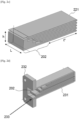
- FIG. 2a represents the principles inherent in a charge 200 according to the invention.
- the vertical arrows represent the amplitude of the electric field.
- the load 200 comprises a transmission line 201 implemented in the form of a waveguide of width L , height h ' and length /.
- the waveguide 201 is terminated by a partition, which creates a short circuit at the end of the transmission line.
- the height h ' of the waveguide 201 is less than the height h of the waveguide to be terminated.
- the height h ' and the length / of the waveguide 201 are therefore chosen according to the adaptation sought by the load, the adaptation being the capacity of the load to absorb energy, taking into account the operating frequency and the conductivity of the metal used for the waveguide.
- the waveguide 201 will have a length much greater than the wavelength ⁇ of the signals received from the waveguide, for example greater than ten times the wavelength, and advantageously greater than fifteen times the wavelength.
- the load 201 also comprises a variable height transmission line 202, better known by the English term taper, configured to carry out the impedance matching between the waveguide to be terminated and the waveguide 201. Indeed, without impedance matching between the two guides of different heights, part of the electromagnetic waves would be reflected by the load, which would then not play its role as a power absorber.
- a variable height transmission line 202 better known by the English term taper
- the load may or may not be equipped with a fixing means such as a flange (not shown).
- the invention can be implemented by connecting this waveguide to an ellipsoidal waveguide whose dimension is reduced along at least one axis (the width of the waveguide to be terminated having to be maintained over the entire path of the wave so that it propagates).
- the all-metal load 200 can be made of a metal or metal alloy having high conductivity losses, such as for example titanium or Inconel TM .
- the waveguides are generally made of aluminum, which has good conductivity properties and a low weight. The propagation losses increase when the conductivity of the support decreases.
- the losses of the load according to the invention are therefore increased.
- the size l of the waveguide 201 in a load according to the invention is divided by two between an aluminum waveguide (electrical conductivity of 36.9 MSiemens/m) and a titanium guide (electrical conductivity of 2.4 MSiemens/m).
- the load 200 can be designed in a metal treated so as to degrade the porosity thereof.
- the load can be designed by an additive manufacturing technique.
- Additive manufacturing is the design of three-dimensional metal parts from successive thin layers of metal powder melted by a laser beam coupled to a CAD model of the part to be produced. The part is then built layer by layer, unlike machining, which proceeds by removing material. This is the equivalent of 3D printing for metal.
- Additive manufacturing makes it possible to quickly and easily design metal parts with degraded porosity (Ra), with conductivity typically reduced by a factor of 5 to 10. This degradation of the porosity of the charge reduces the equivalent conductivity of the metal used to produce the charge, which further increases losses and corresponds to the desired objective.
- the porosity of the filler can also be artificially degraded by additive manufacturing, or by any other method, such as using chemical treatments.
- the load 200 according to the invention therefore meets the expressed need to thermally dissipate the electromagnetic energy supplied to it. Rather than absorbing it, the energy is directly dissipated by a metal waveguide exhibiting significant losses.
- the size of the load mainly linked to the length of the waveguide 201, does not allow simple use of the load.
- FIG. 2b represents a first embodiment of the invention, comparable to that of the Figure 2a , but in which the waveguide 211 is folded back on itself so as to form meanders.
- the arrangement of the waveguide 211 makes it possible to reduce the dimensions of the load 200.
- the waveguide 211 still has a length / when unfolded, but the folds allow it to occupy only a length equivalent to l ' less than l .
- This embodiment is therefore equivalent to that of the Figure 1 in terms of performance, while being more compact.
- FIG. 2c represents another embodiment of a load according to the invention. This differs from the embodiment presented in Figure 2b in that the waveguide 221 is folded back on itself and occupies the spaces freed up above the variable height transmission line 202. This embodiment makes it possible to further reduce the length /" occupied by the waveguide 221. Indeed, the folding of the waveguide 221 is not governed by any particular rule, which allows the waveguide 221 to be arranged in unused areas of the equipment.
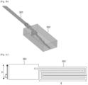
- FIG. 2d represents a longitudinal sectional view of an embodiment of the invention in which the load comprises a flange 232 for flange-to-flange attachment with the waveguide to be terminated.
- the waveguide 231 is folded and occupies the free spaces under the variable-height transmission line 202. It ends at 233 at the flange 232, and does not have a final partition.
- the final partition of the waveguide 231, which short-circuits the transmission line, is formed by the flange of the waveguide to be terminated, when connecting the load.
- This embodiment is particularly advantageous when the load is produced by additive manufacturing. Indeed, this manufacturing method can leave powder residues in the waveguide 231, which modify the propagation properties and therefore the performances, in uncontrolled proportions.
- the embodiment of the figure 2d allows these powder residues to be evacuated after manufacturing, for example by injecting air or a liquid under pressure through the variable height transmission line 202, the air or liquid passing through the entire waveguide 231 before being expelled through the orifice 233.
- figure 2e represents a view showing all the edges of the load of the figure 2d .
- FIG. 2f gives an example of the absorption performance of a load according to an embodiment corresponding to that of the figure 2d .
- the results are measured in the case of a waveguide in WR51 technology on the Ka frequency band (measured here between 17.75 GHz and 21.25 GHz).
- the load according to the invention has an adaptation greater than 20 dB over the entire band.
- the load according to the invention can be produced from a single piece, by additive manufacturing, which makes it inexpensive, not very complex to produce, and infinitely replicable from a 3D file.
- any component e.g., a coupler or an antenna feed
- it can be easily integrated into the design of any component (e.g., a coupler or an antenna feed), and can be manufactured jointly with this component. Its shape can then be adapted to that of the component so as to occupy wasted spaces.
- Such joint manufacturing reduces the volume of the assembly, manufacturing costs, and improves the reliability of the component.
- additive manufacturing makes it possible to interweave coils dedicated to the circulation of a cooling liquid directly into the load (for example between the folds of the waveguide 211), in order to improve the dissipation of the thermal energy produced.
- the load is folded back on itself by 180° bends.
- many other ways of folding the transmission line are possible, allowing the same result of reducing the size of the load to be achieved, for example by rolling it on itself in the form of a spiral, or by arranging it in such a way as to form a broken line forming alternately salient and re-entrant angles (zig-zag).
- the load 300 comprises a transmission line 301 in the form of a metallic coaxial cable whose diameter is less than the height h of the waveguide to which the load is connected.
- the coaxial cable is terminated by a short circuit.
- the arrows represent the electric field.
- the length / of the coaxial cable is chosen according to the desired level of adaptation and the conductivity of the coaxial cable.
- the electric field extends between the core and the shielding of the cable.
- the coaxial cable is then advantageously chosen to have the smallest possible gap between the core and the shielding, in order to increase the intensity of the current and voltages propagating inside, and therefore the thermal losses.
- the core of the cable can be made of a low-conductivity material, such as titanium.
- the coaxial cable does not have a dielectric material positioned between the core and the shielding, fixing means ensuring that the core is held in position and preventing contact with the shielding. Satisfactory results have been obtained at 20 GHz with a coaxial cable with a radius of 0.2 mm and a length of 300 mm.
- the load also includes a guide-to-coaxial transition device (TGC) 302 configured to enable the transition between guided propagation along a waveguide and coaxial propagation.
- TGC guide-to-coaxial transition device
- This device further performs impedance matching between the two transmission lines, in order to avoid reflections of electromagnetic waves.
- TGC guide-to-coaxial transition device
- FIG. 3b represents a perspective view of a load terminated by a coaxial cable.
- Figures 3a And 3b has the advantage of being able to be completely metallic. However, its size can be significant.
- FIG. 3c represents an embodiment of a load according to the invention, in which the transmission line is implemented by a coaxial cable.
- the transmission line is implemented by a coaxial cable.
- the latter is folded back on itself, or wound, so as to form one or more meanders.
- This embodiment has the advantage of taking up less space than that of the Figure 3a . Particular care must be taken to avoid short circuits between the core and the shield of the coaxial cable, especially at bends.
- the various embodiments presented of a load according to the invention achieve the desired objectives.
- the metal load according to the invention is either entirely metallic (case of figures 2b to 2g), or made from low-complexity consumer components ( Figure 3c ).
- the invention can be arranged in different ways, each having particular characteristics of performance, manufacturing complexity and compactness.
- the charges according to the invention can be further improved by the use of low-conductivity metals, generally not considered for the manufacture of microwave materials, by producing them using additive manufacturing processes, or by subjecting them to chemical treatments intended to increase their porosity.
- the invention also relates to a method for manufacturing a load by additive manufacturing.
- additive manufacturing makes it possible to quickly and simply design metallic loads having degraded porosity, which is usually problematic but proves advantageous in the context of a load since this degradation of the porosity reduces the equivalent conductivity of the metal used to make the load, which further increases the losses and corresponds to the desired objective.
- the electronic file can be obtained by software modeling (in English Computer Aided Design, or CAD) and/or by scanning the surface of the load to measure its surface configuration (in English scanning).
- Many file formats are possible, such as Stereolithography or "Standard Tessellation Language” type files (.stl files), Additive Manufacturing File (.amf files), AutoCad (.dwg files), Blender (.blend files), Parasolid (.x_t files), 3D Manufacturing Format (.3mf files), Autodesk (3ds files), Collada (.dae files) and Wavefront (.obj files), among others.
- the electronic file can be converted into a set of instructions executable by a processor, allowing it to control an additive manufacturing device in order to produce the load according to the geometric arrangement considered.
- the conversion may consist of converting the file into a set of layers to be sequentially formed by the additive manufacturing device.
- the additive manufacturing device (3D printer) executes the instructions transmitted to it to manufacture the load according to the invention.
- the electronic file can be saved in different formats, and saved on a storage medium capable of being read by a computer.
Landscapes
- Waveguides (AREA)
- Non-Reversible Transmitting Devices (AREA)
Applications Claiming Priority (1)
| Application Number | Priority Date | Filing Date | Title |
|---|---|---|---|
| FR2314166A FR3157017A1 (fr) | 2023-12-14 | 2023-12-14 | Charge pour circuit Hyperfréquence |
Publications (1)
| Publication Number | Publication Date |
|---|---|
| EP4572004A1 true EP4572004A1 (de) | 2025-06-18 |
Family
ID=90811100
Family Applications (1)
| Application Number | Title | Priority Date | Filing Date |
|---|---|---|---|
| EP24218518.9A Pending EP4572004A1 (de) | 2023-12-14 | 2024-12-09 | Last für mikrowellenschaltung |
Country Status (2)
| Country | Link |
|---|---|
| EP (1) | EP4572004A1 (de) |
| FR (1) | FR3157017A1 (de) |
Citations (2)
| Publication number | Priority date | Publication date | Assignee | Title |
|---|---|---|---|---|
| US3940719A (en) * | 1974-10-25 | 1976-02-24 | Raytheon Company | Microwave waveguide dissipative load comprising fluid cooled lossy waveguide section |
| CN117039376A (zh) * | 2023-08-02 | 2023-11-10 | 电子科技大学 | 一种基于磁性金属表面的波导匹配负载 |
-
2023
- 2023-12-14 FR FR2314166A patent/FR3157017A1/fr active Pending
-
2024
- 2024-12-09 EP EP24218518.9A patent/EP4572004A1/de active Pending
Patent Citations (2)
| Publication number | Priority date | Publication date | Assignee | Title |
|---|---|---|---|---|
| US3940719A (en) * | 1974-10-25 | 1976-02-24 | Raytheon Company | Microwave waveguide dissipative load comprising fluid cooled lossy waveguide section |
| CN117039376A (zh) * | 2023-08-02 | 2023-11-10 | 电子科技大学 | 一种基于磁性金属表面的波导匹配负载 |
Also Published As
| Publication number | Publication date |
|---|---|
| FR3157017A1 (fr) | 2025-06-20 |
Similar Documents
| Publication | Publication Date | Title |
|---|---|---|
| FR3074364B1 (fr) | Charge interne pour tube a ondes progressives utilisant une ligne a retard en guide replie | |
| EP0487387B1 (de) | Flache Mikrowellen-Schlitzantenne | |
| EP0575211B1 (de) | Strahlerelement einer Antenne mit breitbandigem Durchlassbereich und aus derartigen Elementen bestehende Gruppenantenne | |
| EP1407512B1 (de) | Antenne | |
| CA2148796C (fr) | Antenne fil-plaque monopolaire | |
| EP3726642B1 (de) | Polarisationsschirm mit breitband-hochfrequenz-polarisationszelle(n) | |
| FR2528633A1 (fr) | Guide d'onde dielectrique | |
| FR2640819A1 (fr) | Cable semi-rigide destine a la transmission des ondes hyperfrequence | |
| EP3136499B1 (de) | Aufteilungs-/kombinationssystem für hyperfrequenzwelle | |
| EP0333568B1 (de) | Mehrweg-Addierer/Verteiler | |
| EP3109941A1 (de) | Mikrowellen-doppelreflektorantenne | |
| EP2365584B1 (de) | Antennenvorrichtung mit einer Planarantenne und einem Breitbandreflektor sowie ein Herstellungsverfahren des Reflektors | |
| EP4572004A1 (de) | Last für mikrowellenschaltung | |
| EP3850707B1 (de) | Spiralsegmentantenne | |
| EP4024604B1 (de) | Magische breitband-mikrowellen-verbindung in t-form | |
| EP4572005A1 (de) | Last für mikrowellenschaltung | |
| EP0769824B1 (de) | Elektomagnetische Linse in Form einer auf einem getragenen Substrat gedruckten Schaltung | |
| BE1011665A5 (fr) | Dispositif d'antennes spirales perfectionné | |
| EP3721501A1 (de) | Mikrowellen-bauelement und zugehöriges herstellungsverfahren | |
| FR2822594A1 (fr) | Antenne plane multicouche comportant un element de connectique orthogonale et son procede de fabrication | |
| FR2461369A1 (fr) | Element coaxial pour hyperfrequences, son procede de realisation, et composant hyperfrequence comprenant un tel element | |
| EP0017562B1 (de) | Festkörper-Mikrowellenquelle | |
| FR2483119A1 (fr) | Element resistif en technique microbande et circuit comportant au moins un tel element | |
| BE525572A (de) | ||
| FR3159270A1 (fr) | Applicateur électromagnétique haute fréquence |
Legal Events
| Date | Code | Title | Description |
|---|---|---|---|
| PUAI | Public reference made under article 153(3) epc to a published international application that has entered the european phase |
Free format text: ORIGINAL CODE: 0009012 |
|
| STAA | Information on the status of an ep patent application or granted ep patent |
Free format text: STATUS: THE APPLICATION HAS BEEN PUBLISHED |
|
| AK | Designated contracting states |
Kind code of ref document: A1 Designated state(s): AL AT BE BG CH CY CZ DE DK EE ES FI FR GB GR HR HU IE IS IT LI LT LU LV MC ME MK MT NL NO PL PT RO RS SE SI SK SM TR |
|
| STAA | Information on the status of an ep patent application or granted ep patent |
Free format text: STATUS: REQUEST FOR EXAMINATION WAS MADE |
|
| 17P | Request for examination filed |
Effective date: 20251121 |