EP4546382A2 - Diskontinuierliche grenzflächenschicht für ein mehrschichtiges keramikbauteil mit einem an aluminium-nickel-legierung reichen bereich, der mit den inneren nickelelektroden in kontakt steht, und einem an kupfer-aluminium-legierung reichen bereich, der mit den äusseren kupferelektroden in kontakt steht - Google Patents
Diskontinuierliche grenzflächenschicht für ein mehrschichtiges keramikbauteil mit einem an aluminium-nickel-legierung reichen bereich, der mit den inneren nickelelektroden in kontakt steht, und einem an kupfer-aluminium-legierung reichen bereich, der mit den äusseren kupferelektroden in kontakt steht Download PDFInfo
- Publication number
- EP4546382A2 EP4546382A2 EP24206659.5A EP24206659A EP4546382A2 EP 4546382 A2 EP4546382 A2 EP 4546382A2 EP 24206659 A EP24206659 A EP 24206659A EP 4546382 A2 EP4546382 A2 EP 4546382A2
- Authority
- EP
- European Patent Office
- Prior art keywords
- region
- disposed
- alloy
- electrodes
- electronic component
- Prior art date
- Legal status (The legal status is an assumption and is not a legal conclusion. Google has not performed a legal analysis and makes no representation as to the accuracy of the status listed.)
- Pending
Links
Images


Classifications
-
- H—ELECTRICITY
- H01—ELECTRIC ELEMENTS
- H01G—CAPACITORS; CAPACITORS, RECTIFIERS, DETECTORS, SWITCHING DEVICES, LIGHT-SENSITIVE OR TEMPERATURE-SENSITIVE DEVICES OF THE ELECTROLYTIC TYPE
- H01G4/00—Fixed capacitors; Processes of their manufacture
- H01G4/002—Details
- H01G4/228—Terminals
- H01G4/232—Terminals electrically connecting two or more layers of a stacked or rolled capacitor
- H01G4/2325—Terminals electrically connecting two or more layers of a stacked or rolled capacitor characterised by the material of the terminals
-
- H—ELECTRICITY
- H01—ELECTRIC ELEMENTS
- H01G—CAPACITORS; CAPACITORS, RECTIFIERS, DETECTORS, SWITCHING DEVICES, LIGHT-SENSITIVE OR TEMPERATURE-SENSITIVE DEVICES OF THE ELECTROLYTIC TYPE
- H01G4/00—Fixed capacitors; Processes of their manufacture
- H01G4/002—Details
- H01G4/005—Electrodes
- H01G4/008—Selection of materials
-
- H—ELECTRICITY
- H01—ELECTRIC ELEMENTS
- H01G—CAPACITORS; CAPACITORS, RECTIFIERS, DETECTORS, SWITCHING DEVICES, LIGHT-SENSITIVE OR TEMPERATURE-SENSITIVE DEVICES OF THE ELECTROLYTIC TYPE
- H01G4/00—Fixed capacitors; Processes of their manufacture
- H01G4/30—Stacked capacitors
-
- H—ELECTRICITY
- H01—ELECTRIC ELEMENTS
- H01G—CAPACITORS; CAPACITORS, RECTIFIERS, DETECTORS, SWITCHING DEVICES, LIGHT-SENSITIVE OR TEMPERATURE-SENSITIVE DEVICES OF THE ELECTROLYTIC TYPE
- H01G4/00—Fixed capacitors; Processes of their manufacture
- H01G4/002—Details
- H01G4/005—Electrodes
-
- H—ELECTRICITY
- H01—ELECTRIC ELEMENTS
- H01G—CAPACITORS; CAPACITORS, RECTIFIERS, DETECTORS, SWITCHING DEVICES, LIGHT-SENSITIVE OR TEMPERATURE-SENSITIVE DEVICES OF THE ELECTROLYTIC TYPE
- H01G4/00—Fixed capacitors; Processes of their manufacture
- H01G4/002—Details
- H01G4/005—Electrodes
- H01G4/008—Selection of materials
- H01G4/0085—Fried electrodes
-
- H—ELECTRICITY
- H01—ELECTRIC ELEMENTS
- H01G—CAPACITORS; CAPACITORS, RECTIFIERS, DETECTORS, SWITCHING DEVICES, LIGHT-SENSITIVE OR TEMPERATURE-SENSITIVE DEVICES OF THE ELECTROLYTIC TYPE
- H01G4/00—Fixed capacitors; Processes of their manufacture
- H01G4/002—Details
- H01G4/005—Electrodes
- H01G4/012—Form of non-self-supporting electrodes
-
- H—ELECTRICITY
- H01—ELECTRIC ELEMENTS
- H01G—CAPACITORS; CAPACITORS, RECTIFIERS, DETECTORS, SWITCHING DEVICES, LIGHT-SENSITIVE OR TEMPERATURE-SENSITIVE DEVICES OF THE ELECTROLYTIC TYPE
- H01G4/00—Fixed capacitors; Processes of their manufacture
- H01G4/002—Details
- H01G4/018—Dielectrics
- H01G4/06—Solid dielectrics
- H01G4/08—Inorganic dielectrics
- H01G4/12—Ceramic dielectrics
-
- H—ELECTRICITY
- H01—ELECTRIC ELEMENTS
- H01G—CAPACITORS; CAPACITORS, RECTIFIERS, DETECTORS, SWITCHING DEVICES, LIGHT-SENSITIVE OR TEMPERATURE-SENSITIVE DEVICES OF THE ELECTROLYTIC TYPE
- H01G4/00—Fixed capacitors; Processes of their manufacture
- H01G4/002—Details
- H01G4/228—Terminals
-
- H—ELECTRICITY
- H01—ELECTRIC ELEMENTS
- H01G—CAPACITORS; CAPACITORS, RECTIFIERS, DETECTORS, SWITCHING DEVICES, LIGHT-SENSITIVE OR TEMPERATURE-SENSITIVE DEVICES OF THE ELECTROLYTIC TYPE
- H01G4/00—Fixed capacitors; Processes of their manufacture
- H01G4/002—Details
- H01G4/228—Terminals
- H01G4/232—Terminals electrically connecting two or more layers of a stacked or rolled capacitor
Definitions
- the present disclosure relates to a multilayer electronic component.
- Multilayer Ceramic Capacitors are chip-type condensers mounted on the printed circuit boards of various electronic products such as video devices, for example, liquid crystal displays (LCDs) and plasma display panels (PDPs), computers, smartphones, and mobile phones to charge or discharge electricity therein or therefrom.
- video devices for example, liquid crystal displays (LCDs) and plasma display panels (PDPs)
- LCDs liquid crystal displays
- PDPs plasma display panels
- computers smartphones, and mobile phones to charge or discharge electricity therein or therefrom.
- Multilayer ceramic capacitors may be used as components in various electronic devices due to a small size, high capacitance, and ease of mounting thereof.
- multilayer ceramic capacitors are also trending toward miniaturization and higher capacitance. Accordingly, the importance of ensuring high reliability of multilayer ceramic capacitors is increasing.
- ESR equivalent series resistance
- An aspect of the present disclosure is to provide a multilayer electronic component having relatively high reliability.
- An aspect of the present disclosure is to improve connectivity between internal electrodes and external electrodes.
- a multilayer electronic component includes a body including a dielectric layer and an internal electrode alternately disposed with the dielectric layer; an external electrode disposed on the body and connected to the internal electrode; and a region containing Ni, Al and Cu.
- the internal electrode includes Ni, and the external electrode contains Al and Cu.
- a multilayer electronic component includes a body including a dielectric layer and internal electrodes alternately disposed with the dielectric layer; and an external electrode disposed on the body and including a base electrode layer connected to the internal electrodes.
- the base electrode layer includes Al, Cu, and glass.
- the first direction may be defined as the stacking or thickness (T) direction
- the second direction may be defined as the length (L) direction
- the third direction may be defined as the width (W) direction.
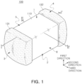
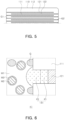
- FIG. 1 schematically illustrates a perspective view of a multilayer electronic component according to an embodiment.
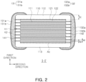
- FIG. 2 schematically illustrates a cross-sectional view taken along line I-I' of FIG. 1 .
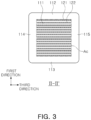
- FIG. 3 schematically illustrates a cross-sectional view taken along line II-II' of FIG. 1 .
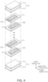
- FIG. 4 schematically illustrates a body in a disassembled state.
- FIG. 5 schematically illustrates a portion of the body of FIG. 2 .
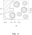
- FIG. 6 is an enlarged view illustrating area K1 of FIG. 2 .
- FIG. 7 is an enlarged view illustrating area K1 of FIG. 2 according to an alternate embodiment.
- a multilayer electronic component 100 according to an embodiment will be described in detail with reference to FIGS. 1 to 7 .
- a multilayer ceramic capacitor hereinafter referred to as an 'MLCC'
- the present disclosure is not limited thereto, and may also be applied to various multilayer electronic components using ceramic materials, such as inductors, piezoelectric elements, varistors, thermistors, or the like.
- the multilayer electronic component 100 may include a body 110 including a dielectric layer 111 and first and second internal electrodes 121 and 122 alternately disposed with the dielectric layer, and first and second external electrodes 131 and 132 disposed on the body and connected to the internal electrodes, and may include regions 141 and 142 containing Ni, Al and Cu.
- the internal electrodes may include Ni
- the external electrodes may include Al and Cu.
- the connectivity between external and internal electrodes has a significant impact on the reliability of multilayer electronic components.
- the electrical connectivity between the internal and external electrodes decreases, which may increase the equivalent series resistance (ESR), and when high voltage is applied, defects such as arc burn may occur.
- ESR equivalent series resistance
- the reliability of the multilayer electronic component may be improved by improving the connectivity between the internal electrode and the external electrode by including regions 141 and 142 containing Ni, Al, and Cu.
- the body 110 may have dielectric layers 111 and the first and second internal electrodes 121 and 122 alternately stacked.
- the body 110 may have a hexahedral or similar shape. Due to shrinkage of the ceramic powder particles contained in the body 110 during the sintering process, the body 110 may not have a hexahedral shape with completely straight lines, but may have a substantially hexahedral shape.
- the body 110 may have first and second surfaces 1 and 2 opposing in a first direction, third and fourth surfaces 3 and 4 connected to the first and second surfaces 1 and 2 and opposing in a second direction, and fifth and sixth surfaces 5 and 6 connected to the first and second surfaces 1 and 2, connected to the third and fourth surfaces 3 and 4, and opposing in a third direction.
- a corner connecting the first surface and the third to fifth surfaces and/or a corner connecting the second surface and the third to fifth surfaces may have a shape contracted toward the center of the body 110 in the first direction when viewed from the first or second surface.
- a corner connecting the first surface 1 and the third to sixth surfaces 3, 4, 5 and 6 and/or corners connecting the second surface 2 and the third to sixth surfaces 3, 4, 5 and 6 may have a shape contracted toward the center of the body 110 in the first direction when viewed from the first or second surface.
- the edges connecting respective surfaces of the body 110 are rounded by performing a separate process.
- the corner connecting the first surface and the third to sixth surfaces and/or the corner connecting the second surface and the third to sixth surfaces may have a rounded shape.
- the internal electrodes are cut to be exposed to the fifth and sixth surfaces 5 and 6 of the body, and then, when forming first and second margin portions 114 and 115 by stacking a single dielectric layer or two or more dielectric layers on both sides of the capacitance formation portion Ac in the third direction (width direction), the portion connecting the first surface to the fifth and sixth surfaces and the portion connecting the second surface to the fifth and sixth surfaces may not have a contracted shape.
- the plurality of dielectric layers 111 forming the body 110 are in a sintered state, and the boundaries between adjacent dielectric layers 111 may be integrated to the extent that it may be difficult to determine without using a scanning electron microscope (SEM).
- SEM scanning electron microscope
- the number of stacked dielectric layers does not need to be particularly limited and may be determined considering the size of the multilayer electronic component.
- the body may be formed by stacking 400 or more dielectric layers.
- the dielectric layer 111 may be formed by producing a ceramic slurry containing ceramic powder, an organic solvent, and a binder, applying and drying the slurry on a carrier film to prepare a ceramic green sheet, and then by firing the ceramic green sheet.
- Ceramic powder is not particularly limited as long as sufficient capacitance may be obtained.
- a barium titanate (BaTiO 3 )-based powder may be used as the ceramic powder.
- ceramic powder may be at least one of BaTiO 3 , (Ba 1-x Ca x )TiO 3 (0 ⁇ x ⁇ 1), Ba(Ti 1-y Ca y )O 3 (0 ⁇ y ⁇ 1), (Ba 1-x Ca x )(Ti 1-y 2r y )O 3 (0 ⁇ x ⁇ 1, 0 ⁇ y ⁇ 1) and Ba(Ti 1-y Zr y )O 3 (0 ⁇ y ⁇ 1).
- the average thickness td of the dielectric layer 111 does not need to be particularly limited, but may be, for example, 0.01 um to 10 um.
- the average thickness td of the dielectric layer 111 may be arbitrarily set depending on the required characteristics or use. For example, in the case of small IT electronic components, the average thickness td of at least one of the plurality of dielectric layers 111 may be 1.5 um or less to obtain miniaturization and high capacitance.
- the average thickness td of the dielectric layer 111 may refer to the size of the dielectric layer 111 disposed between the first and second internal electrodes 121 and 122 in the first direction.
- the average thickness of the dielectric layer 111 may be measured by scanning cross-sections of the body 110 in the first and second directions with a scanning electron microscope (SEM) at a magnification of 10,000.
- SEM scanning electron microscope
- the average value may be measured by measuring the thickness at multiple points of one dielectric layer 111, for example, 30 points at equal intervals in the second direction. The 30 equally spaced points may be designated in the capacitance formation portion Ac, which will be described later. Additionally, if this average value measurement is expanded to 10 dielectric layers 111 and the average value is measured, the average thickness of the dielectric layers 111 may be further generalized.
- the body 110 may include a capacitance formation portion (Ac), which is disposed inside the body 110 and in which capacitance is formed by including a first internal electrode 121 and a second internal electrode 122 disposed to face each other with the dielectric layer 111 interposed therebetween, and cover portions 112 and 113 formed above and below the capacitance formation portion Ac in the first direction.
- Ac capacitance formation portion
- the capacitance formation portion (Ac) is a part that contributes to forming the capacitance of the capacitor, and may be formed by repeatedly stacking a plurality of first and second internal electrodes 121 and 122 with the dielectric layer 111 interposed therebetween.
- the cover portions 112 and 113 may include an upper cover portion 112 disposed above the capacitance formation portion Ac in the first direction and a lower cover portion 113 disposed below the capacitance formation portion Ac in the first direction.
- the upper cover portion 112 and the lower cover portion 113 may be formed by stacking a single dielectric layer or two or more dielectric layers on the upper and lower surfaces of the capacitance formation portion Ac in the thickness direction, respectively, and basically, may play a role in preventing damage to the internal electrodes due to physical or chemical stress.
- the upper cover portion 112 and the lower cover portion 113 do not include internal electrodes and may include the same material as the dielectric layer 111.
- the upper cover portion 112 and the lower cover portion 113 may include a ceramic material, for example, a barium titanate (BaTiO 3 )-based ceramic material.
- a ceramic material for example, a barium titanate (BaTiO 3 )-based ceramic material.
- the thickness of the cover portions 112 and 113 does not need to be particularly limited. However, to more easily obtain miniaturization and high capacitance of the multilayer electronic component, the thickness tc of the cover portions 112 and 113 may be 60 ⁇ m or less.
- the average thickness tc of the cover portions 112 and 113 may refer to the size in the first direction, and may be an average value of sizes of the cover portions 112 and 113 in the first direction, measured at five points at equal intervals above or below the capacitance formation portion Ac.
- first and second margin portions 114 and 115 may be disposed on the sides of the capacitance formation portion Ac.
- the first and second margin portions 114 and 115 may include a first margin portion 114 disposed on the fifth surface 5 of the body 110 and a second margin portion 115 disposed on the sixth surface 6.
- the first and second margin portions 114 and 115 may be disposed on both end surfaces of the ceramic body 110 in the width direction.
- the first and second margin portions 114 and 115 may refer to the area between both ends of the first and second internal electrodes 121 and 122 and the boundary surface of the body 110 in a cross-section of the body 110 in the width-thickness (W-T) direction.
- the first and second margin portions 114 and 115 may basically serve to prevent damage to the internal electrodes due to physical or chemical stress.
- the first and second margin portions 114 and 115 may be formed by forming internal electrodes by applying conductive paste on a ceramic green sheet except for areas in which the margin portion is to be formed.
- the internal electrodes are cut to be exposed to the fifth and sixth surfaces 5 and 6 of the body, and then a single dielectric layer or two or more dielectric layers may be stacked on both sides of the capacitance formation portion Ac in the third direction (width direction) to form the first and second margin portions 114 and 115.
- the width of the first and second margin portions 114 and 115 does not need to be particularly limited. However, to more easily obtain miniaturization and high capacitance of multilayer electronic components, the average width of the first and second margin portions 114 and 115 may be 45 um or less.
- the average width of the first and second margin portions 114 and 115 may refer to the average size of the area in which the internal electrode is spaced apart from the fifth surface in the third direction and the average size of the area in which the internal electrode is spaced apart from the sixth surface in the third direction, and may be an average value of sizes of the first and second margin portions 114 and 115 in the third direction, measured at five points at equal intervals on the side of the capacitance formation portion Ac.
- the average size of the areas in which the first and second internal electrodes 121 and 122 are spaced apart from the fifth and sixth surfaces in the third direction may each be 45 um or less.
- the multilayer electronic component when a magnetic material is applied to the body 110 instead of a dielectric material, the multilayer electronic component may function as an inductor.
- the magnetic material may be, for example, ferrite and/or metallic magnetic particles.
- the internal electrode may be a coiled conductor.
- the multilayer electronic component may function as a piezoelectric element.
- the piezoelectric material may be, for example, lead zirconate titanate (PZT).
- the multilayer electronic component may function as a varistor.
- the multilayer electronic component may function as a thermistor.
- the multilayer electronic component 100 may function as an inductor, piezoelectric element, varistor, or thermistor as well as a multilayer ceramic capacitor by appropriately changing the material or structure of the body 110.
- the first and second internal electrodes 121 and 122 may be disposed alternately with the dielectric layer 111, and for example, the first internal electrode 121 and the second internal electrode 122, which are a pair of electrodes having different polarities, may be disposed to face each other with the dielectric layer 111 interposed therebetween.
- the first internal electrode 121 and the second internal electrode 122 may be electrically separated from each other by the dielectric layer 111 disposed therebetween. In this case, the first and second internal electrodes 121 and 122 may be alternately disposed with the dielectric layer 111 in the first direction.
- the first internal electrode 121 may be spaced apart from the fourth surface 4, but may extend toward the third surface 3.
- the second internal electrode 122 may be spaced apart from the third surface 3, but may extend toward the fourth surface 4.
- the first internal electrode 121 may be electrically connected to the first external electrode 131 on the third surface 3, and the second internal electrode 122 may be electrically connected to the second external electrode 132 on the fourth surface 4.
- the conductive metal included in the first and second internal electrodes 121 and 122 may be at least one of Ni, Cu, Pd, Ag, Au, Pt, Sn, W, Ti, and alloys thereof.
- the first and second internal electrodes 121 and 122 may include Ni.
- the first and second internal electrodes 121 and 122 may contain Ni, an Al and Ni alloy may be easily formed in the regions 141 and 142 containing Ni, Al and Cu when forming the base electrode layers 131a and 132a.
- the first and second internal electrodes 121 and 122 may contain Ni as a main component, and in this case, including Ni as the main component may indicate that when the cross section of the internal electrode is analyzed by SEM-EDS, the area ratio occupied by Ni compared to the total area of the internal electrode is 90% or more.
- the method of forming the first and second internal electrodes 121 and 122 is not particularly limited.
- the first and second internal electrodes 121 and 122 may be formed by applying a conductive paste for internal electrodes containing a conductive metal on a ceramic green sheet and firing the same.
- the method of applying the conductive paste for internal electrodes may be screen printing, gravure printing, or the like, but the present disclosure is not limited thereto.
- the average thickness te of the first and second internal electrodes 121 and 122 does not need to be particularly limited, but may be, for example, 0.01 um to 3 um.
- the average thickness te of the first and second internal electrodes 121 and 122 may be arbitrarily set depending on required characteristics or use. For example, in the case of small IT electronic components, to obtain miniaturization and high capacitance, the average thickness te of at least one of the plurality of internal electrodes 121 and 122 may be 0.8 um or less.
- the average thickness te of the internal electrode may be measured by scanning a cross-section of the body 110 in the first and second directions with a scanning electron microscope (SEM) at 10,000 magnification.
- the average value may be measured by measuring the thickness at multiple points of one internal electrode (121, 122), for example, at 30 points at equal intervals in the second direction. The 30 equally spaced points may be designated in the capacitance formation portion (Ac). Additionally, if this average value measurement is expanded to 10 first and second internal electrodes 121 and 122 and the average value is measured, the average thickness of the first and second internal electrodes 121 and 122 may be further generalized.
- the regions 141 and 142 containing Ni, Al, and Cu may be disposed between the first and second internal electrodes 121 and 122 and the first and second external electrodes 131 and 132.
- the regions 141 and 142 containing Ni, Al and Cu may include a region 141 including first Ni, Al, and Cu disposed between the first internal electrode 121 and the first external electrode 131, and a region 142 containing second Ni, Al, and Cu disposed between the second internal electrode 122 and the second external electrode 132.
- Al may stably form alloys with Ni and Cu.
- the melting point of Al is about 660 °C, which is lower than the sintering temperature of general sintering electrodes, and thus, it is easy to improve the connectivity between the first and second external electrodes 131 and 132 and the first and second internal electrodes 121 and 122 when forming the first and second external electrodes 131 and 132.
- FIG. 6 is an enlarged view illustrating the K1 area of FIG. 2 .
- FIG. 7 is a diagram corresponding to FIG. 6 according to an embodiment.
- FIG. 8 is a diagram corresponding to FIG. 6 according to another embodiment.
- the K1 area is an enlarged illustration of a portion of the first external electrode 131, the region 141 containing first Ni, Al and Cu, and a portion of the first internal electrode 121.
- the only difference is that the first external electrode 131 is disposed on the third surface, and the second external electrode 132 is disposed on the fourth surface, and since the configurations of the first external electrode 131 and the second external electrode 132 are similar, the description below will be based on the first external electrode 131, but this will be considered to include the description of the second external electrode 132.
- regions 141 and 142 containing Ni, Al and Cu and the first and second internal electrodes 121 and 122 are also described based on the region 141 containing first Ni, Al and Cu and the first internal electrode 121, but this is considered to include a description of the region 142 including second Ni, Al, and Cu and the second internal electrode 122.
- an Al-Ni alloy may be disposed in the first region P1
- an Al-Cu alloy may be disposed in the second region P2.
- the region 141 containing Ni, Al, and Cu may be formed of Al-Ni alloy and Al-Cu alloy. Referring to FIG. 6 , the region 141 containing Ni, Al, and Cu may be composed of two layers including the first region P1 formed of Al-Ni alloy and the second region P2 formed of Al-Cu alloy.
- the Ni content of the first region P1 decreases in the direction from the first internal electrode 121 to the first external electrode 131
- the Cu content of the second region P2 may decrease in the direction from the first external electrode 131 to the first internal electrode 121.
- the Al content of the first region P1 increases from the first internal electrode 121 to the first external electrode 131
- the Al content of the second region P2 may increase in the direction from the first external electrode 131 to the first internal electrode 121. Accordingly, the Al content may have a maximum value at the boundary between the first region P1 and the second region P2.
- the first region P1 may be disposed inside the body 110, and at least a portion of the second region P2 may be disposed outside the body 110.
- the first region P1 may be disposed inside the body 110 to contact the end of the first internal electrode 121, and the second region P2 may be disposed to contact the base electrode layer 131a outside the body 110.
- the body 110 may include grooves G1 and G2 where the ends of the first and second internal electrodes 121 and 122 are spaced apart from one surface of the body 110.
- the grooves G1 and G2 may be formed by differences in shrinkage behavior between the first and second internal electrodes 121 and 122 and the dielectric layer 111 during the sintering process of the body 110.
- the firing shrinkage rate of the first and second internal electrodes 121 and 122 is greater than the firing shrinkage rate of the dielectric layer 111, a problem may occur in which the connectivity between the first and second internal electrodes 121 and 122 and the first and second external electrodes 131 and 132 is reduced due to the grooves G1 and G2.
- the first region P1 is disposed to contact the end of the first internal electrode 121 within the grooves G1 and G2, and at least a portion of the second region P2 may be disposed within the grooves G1 and G2, and the remaining area of the second region P2 may be disposed outside the body 110.
- the Al content of the intermediate region Pc' may be higher than the Al content of the first and second regions P1' and P2'.
- the intermediate region Pc' may not include Ni and Cu and may be substantially formed of Al.
- the intermediate region Pc' may have an Al content of 99 at% or more, and at least a portion of the intermediate region Pc' may have an Al content of 100 at% or more.
- the intermediate region Pc' does not necessarily need to be formed of Al, and in an embodiment, a Ni-Al-Cu alloy may be disposed in the intermediate region Pc'.
- the Al content may decrease as it approaches the first region P1' and the second region P2' from the central portion of the intermediate region Pc'.
- the Ni content may decrease and the Cu content may increase as it moves from the boundary between the first region P1' and the intermediate region Pc' to the boundary between the second region P2' and the intermediate region Pc' .
- the plating layers 131b and 132b may serve to improve mounting characteristics.
- the types of plating layers 131b and 132b are not particularly limited, and may be a plating layer containing at least one of Ni, Sn, Pd, and alloys thereof, and may be formed of multiple layers.
- the plating layers 131b and 132b may be Ni plating layers or Sn plating layers, and may be in the form in which a Ni plating layer and a Sn plating layer are formed sequentially on the base electrode layers 131a and 132a, and may be in the form in which the Sn plating layer, Ni plating layer, and Sn plating layer are formed sequentially. Additionally, the plating layers 131b and 132b may include a plurality of Ni plating layers and/or a plurality of Sn plating layers.
- the first and second external electrodes 131 and 132 include Ni plating layers 131b1 and 132b1 disposed on the base electrode layers 131a and 132a, and Al and Al-Ni alloy may be disposed in at least a portion of the interface area between the base electrode layers 131a and 132a and the Ni plating layers 131b1 and 132b1.
- Al (Mz) disposed at the interface area between the base electrode layer 131a and the Ni plating layer 131b1 may be disposed over a portion of the base electrode layer 131a and a portion of the Ni plating layer 131b1.
- Al-Cu alloy (M3a) may be disposed in the area in contact with Cu (M1), and in the portion disposed on the Ni plating layer 131b1 in the Al (Mz) disposed in the interface area between the base electrode layer 131a and the Ni plating layer 131b1, Al-Ni alloy (M3b) may be disposed in a portion in contact with the Ni plating layer 131b1. Accordingly, Al (Mz) may be disposed to be at least partially covered by a layer M3' including Al-Cu alloy (M3a) and Al-Ni alloy (M3b).
- an Sn plating layer 131b2 may be further disposed on the Ni plating layer 131b1.
- the external electrodes 131' and 132' may include conductive resin layers 131c' and 132c' disposed on the base electrode layers 131a' and 132a' and containing conductive particles and resin. Additionally, the external electrodes 131' and 132' may further include plating layers 131b' and 132b' disposed on the conductive resin layers 131c' and 132c'.
- examples of the conductive particles Mf may include Cu, Ni, Sn, Pd, Pt, Au, Ag, Pb and/or alloys thereof, and the like, and in more detail, may include at least one of Cu, Ag, Sn, and alloys thereof.
- the conductive resin layers 131c' and 132c' serve to electrically connect the plating layers 131b' and 132b' and the base electrode layers 131a' and 132a', and may absorb tensile stress generated in a mechanical or thermal environment to prevent cracks from occurring when mounting electronic components on a board, and may serve to protect multilayer electronic components from the bending impact of the substrate.
- the resin Rs included in the conductive resin layers 131c' and 132c' may include a thermosetting resin having electrical insulation properties.
- thermosetting resin may be, for example, an epoxy resin, and the present disclosure is not limited thereto.
- the thermosetting resin may be a bisphenol A resin, glycol epoxy resin, Noblac epoxy resin, or a derivative thereof that has a low molecular weight and is liquid at room temperature.
- the conductive particles Mf included in the conductive resin layers 131c' and 132c' are Cu particles, and Al and Al-Cu alloy may be disposed in at least a portion of the interface area between the base electrode layers 131a' and 132a' and the conductive resin layers 131c' and 132c'.
- Al contained in the base electrode layer 131a' diffuses into the interface area with the conductive resin layer 131c', and a portion of the diffused Al may form Al-Cu alloy (M3) with Cu particles Mf included in the conductive resin layer 131c'.
- Al (M2) has good wettability with the Cu particles Mf among the Cu particles Mf and the resin (Rs), and thus, has a high probability of diffusing toward the Cu particles Mf, and may be difficult to be distinguished due to having a similar shape to Al disposed in the base electrode layer 131a'. Additionally, it may be difficult to clearly distinguish the boundary between the Cu particles Mf included in the conductive resin layer 131c' and the Cu (M1) included in the base electrode layer 131a'.
- the multilayer electronic component 100 may include a body 110 including a dielectric layer 111 and the first and second internal electrodes 121 and 122 alternately disposed with the dielectric layer, and first and second external electrodes 131 and 132 disposed on the body 110 and including base electrode layers 131a and 132a connected to the internal electrodes.
- the base electrode layer may include Al, Cu, and glass.
- the base electrode layers 131a and 132a further contain Al in addition to Cu and glass, Al is melted during the sintering process and may easily fill the empty space between the internal electrodes and the external electrodes, and may stably form an alloy with Ni and Cu, and thus, the connectivity between the base electrode layers 131a and 132a and the first and second internal electrodes 121 and 122 may be improved.
- Al may partially replace the role of glass during the sintering process, thereby lowering the glass content and thereby lowering equivalent series resistance (ESR).
Landscapes
- Engineering & Computer Science (AREA)
- Power Engineering (AREA)
- Manufacturing & Machinery (AREA)
- Microelectronics & Electronic Packaging (AREA)
- Chemical & Material Sciences (AREA)
- Ceramic Engineering (AREA)
- Inorganic Chemistry (AREA)
- Materials Engineering (AREA)
- Fixed Capacitors And Capacitor Manufacturing Machines (AREA)
- Ceramic Capacitors (AREA)
Applications Claiming Priority (2)
| Application Number | Priority Date | Filing Date | Title |
|---|---|---|---|
| KR20230144625 | 2023-10-26 | ||
| KR1020230197417A KR20250060789A (ko) | 2023-10-26 | 2023-12-29 | 적층형 전자 부품 |
Publications (2)
| Publication Number | Publication Date |
|---|---|
| EP4546382A2 true EP4546382A2 (de) | 2025-04-30 |
| EP4546382A3 EP4546382A3 (de) | 2025-11-12 |
Family
ID=93150235
Family Applications (1)
| Application Number | Title | Priority Date | Filing Date |
|---|---|---|---|
| EP24206659.5A Pending EP4546382A3 (de) | 2023-10-26 | 2024-10-15 | Diskontinuierliche grenzflächenschicht für ein mehrschichtiges keramikbauteil mit einem an aluminium-nickel-legierung reichen bereich, der mit den inneren nickelelektroden in kontakt steht, und einem an kupfer-aluminium-legierung reichen bereich, der mit den äusseren kupferelektroden in kontakt steht |
Country Status (4)
| Country | Link |
|---|---|
| US (1) | US20250140474A1 (de) |
| EP (1) | EP4546382A3 (de) |
| JP (1) | JP2025074045A (de) |
| CN (1) | CN119905351A (de) |
Family Cites Families (2)
| Publication number | Priority date | Publication date | Assignee | Title |
|---|---|---|---|---|
| JP7338554B2 (ja) * | 2020-05-20 | 2023-09-05 | Tdk株式会社 | セラミック電子部品 |
| JP2023013238A (ja) * | 2021-07-15 | 2023-01-26 | Tdk株式会社 | セラミック電子部品 |
-
2024
- 2024-10-10 US US18/911,956 patent/US20250140474A1/en active Pending
- 2024-10-15 EP EP24206659.5A patent/EP4546382A3/de active Pending
- 2024-10-23 JP JP2024186967A patent/JP2025074045A/ja active Pending
- 2024-10-25 CN CN202411497759.5A patent/CN119905351A/zh active Pending
Also Published As
| Publication number | Publication date |
|---|---|
| CN119905351A (zh) | 2025-04-29 |
| JP2025074045A (ja) | 2025-05-13 |
| US20250140474A1 (en) | 2025-05-01 |
| EP4546382A3 (de) | 2025-11-12 |
Similar Documents
| Publication | Publication Date | Title |
|---|---|---|
| US10347421B2 (en) | Multilayer ceramic electronic component and method of manufacturing the same | |
| KR101952843B1 (ko) | 내부전극용 도전성 페이스트 조성물 및 이를 포함하는 적층 세라믹 전자부품 | |
| US11164700B2 (en) | Multilayer capacitor | |
| KR102881359B1 (ko) | 적층형 커패시터 | |
| CN115116746B (zh) | 电容器组件 | |
| KR102703774B1 (ko) | 적층 세라믹 전자부품 | |
| KR20130111752A (ko) | 내부전극용 도전성 페이스트 조성물 및 이를 포함하는 적층 세라믹 전자부품 | |
| CN114520115A (zh) | 多层电子组件 | |
| KR102048091B1 (ko) | 적층 세라믹 전자 부품 및 그 제조 방법 | |
| CN115188588A (zh) | 多层电容器和其上安装有多层电容器的基板 | |
| EP4542598A1 (de) | Mehrschichtiges elektronisches bauteil | |
| CN111009415B (zh) | 陶瓷电子组件 | |
| EP4546382A2 (de) | Diskontinuierliche grenzflächenschicht für ein mehrschichtiges keramikbauteil mit einem an aluminium-nickel-legierung reichen bereich, der mit den inneren nickelelektroden in kontakt steht, und einem an kupfer-aluminium-legierung reichen bereich, der mit den äusseren kupferelektroden in kontakt steht | |
| US20160314902A1 (en) | Multilayer ceramic capacitor and method of manufacturing the same | |
| EP4401104A2 (de) | Mehrschichtiges elektronisches bauteil | |
| KR20220081633A (ko) | 적층형 전자 부품 및 유전체 조성물 | |
| KR102900301B1 (ko) | 적층형 전자 부품 | |
| KR20250060789A (ko) | 적층형 전자 부품 | |
| EP4535381A1 (de) | Keramischer mehrschichtiger kondesator | |
| EP4579705A1 (de) | Mehrschichtiges elektronisches bauteil | |
| EP4521432A1 (de) | Elektronisches multilayerbauelement | |
| EP4415012A1 (de) | Mehrschichtiges elektronisches bauteil | |
| EP4579700A1 (de) | Mehrschichtiges elektronisches bauteil | |
| KR20190019117A (ko) | 내부전극용 도전성 페이스트 조성물 및 이를 포함하는 적층 세라믹 전자부품 | |
| KR20250068883A (ko) | 적층형 전자 부품 |
Legal Events
| Date | Code | Title | Description |
|---|---|---|---|
| PUAI | Public reference made under article 153(3) epc to a published international application that has entered the european phase |
Free format text: ORIGINAL CODE: 0009012 |
|
| STAA | Information on the status of an ep patent application or granted ep patent |
Free format text: STATUS: THE APPLICATION HAS BEEN PUBLISHED |
|
| AK | Designated contracting states |
Kind code of ref document: A2 Designated state(s): AL AT BE BG CH CY CZ DE DK EE ES FI FR GB GR HR HU IE IS IT LI LT LU LV MC ME MK MT NL NO PL PT RO RS SE SI SK SM TR |
|
| PUAL | Search report despatched |
Free format text: ORIGINAL CODE: 0009013 |
|
| AK | Designated contracting states |
Kind code of ref document: A3 Designated state(s): AL AT BE BG CH CY CZ DE DK EE ES FI FR GB GR HR HU IE IS IT LI LT LU LV MC ME MK MT NL NO PL PT RO RS SE SI SK SM TR |
|
| RIC1 | Information provided on ipc code assigned before grant |
Ipc: H01G 4/008 20060101AFI20251007BHEP Ipc: H01G 4/012 20060101ALI20251007BHEP Ipc: H01G 4/12 20060101ALI20251007BHEP Ipc: H01G 4/232 20060101ALI20251007BHEP Ipc: H01G 4/30 20060101ALI20251007BHEP |