EP4579705A1 - Mehrschichtiges elektronisches bauteil - Google Patents
Mehrschichtiges elektronisches bauteil Download PDFInfo
- Publication number
- EP4579705A1 EP4579705A1 EP24218112.1A EP24218112A EP4579705A1 EP 4579705 A1 EP4579705 A1 EP 4579705A1 EP 24218112 A EP24218112 A EP 24218112A EP 4579705 A1 EP4579705 A1 EP 4579705A1
- Authority
- EP
- European Patent Office
- Prior art keywords
- disposed
- electronic component
- lead
- multilayer electronic
- glass
- Prior art date
- Legal status (The legal status is an assumption and is not a legal conclusion. Google has not performed a legal analysis and makes no representation as to the accuracy of the status listed.)
- Pending
Links
Images
Classifications
-
- H—ELECTRICITY
- H01—ELECTRIC ELEMENTS
- H01G—CAPACITORS; CAPACITORS, RECTIFIERS, DETECTORS, SWITCHING DEVICES, LIGHT-SENSITIVE OR TEMPERATURE-SENSITIVE DEVICES OF THE ELECTROLYTIC TYPE
- H01G4/00—Fixed capacitors; Processes of their manufacture
- H01G4/002—Details
- H01G4/005—Electrodes
- H01G4/012—Form of non-self-supporting electrodes
-
- H—ELECTRICITY
- H01—ELECTRIC ELEMENTS
- H01G—CAPACITORS; CAPACITORS, RECTIFIERS, DETECTORS, SWITCHING DEVICES, LIGHT-SENSITIVE OR TEMPERATURE-SENSITIVE DEVICES OF THE ELECTROLYTIC TYPE
- H01G4/00—Fixed capacitors; Processes of their manufacture
- H01G4/002—Details
- H01G4/224—Housing; Encapsulation
-
- H—ELECTRICITY
- H01—ELECTRIC ELEMENTS
- H01G—CAPACITORS; CAPACITORS, RECTIFIERS, DETECTORS, SWITCHING DEVICES, LIGHT-SENSITIVE OR TEMPERATURE-SENSITIVE DEVICES OF THE ELECTROLYTIC TYPE
- H01G4/00—Fixed capacitors; Processes of their manufacture
- H01G4/002—Details
- H01G4/018—Dielectrics
- H01G4/06—Solid dielectrics
- H01G4/08—Inorganic dielectrics
- H01G4/12—Ceramic dielectrics
- H01G4/1209—Ceramic dielectrics characterised by the ceramic dielectric material
-
- H—ELECTRICITY
- H01—ELECTRIC ELEMENTS
- H01G—CAPACITORS; CAPACITORS, RECTIFIERS, DETECTORS, SWITCHING DEVICES, LIGHT-SENSITIVE OR TEMPERATURE-SENSITIVE DEVICES OF THE ELECTROLYTIC TYPE
- H01G4/00—Fixed capacitors; Processes of their manufacture
- H01G4/002—Details
- H01G4/228—Terminals
- H01G4/232—Terminals electrically connecting two or more layers of a stacked or rolled capacitor
-
- H—ELECTRICITY
- H01—ELECTRIC ELEMENTS
- H01G—CAPACITORS; CAPACITORS, RECTIFIERS, DETECTORS, SWITCHING DEVICES, LIGHT-SENSITIVE OR TEMPERATURE-SENSITIVE DEVICES OF THE ELECTROLYTIC TYPE
- H01G4/00—Fixed capacitors; Processes of their manufacture
- H01G4/30—Stacked capacitors
-
- H—ELECTRICITY
- H01—ELECTRIC ELEMENTS
- H01G—CAPACITORS; CAPACITORS, RECTIFIERS, DETECTORS, SWITCHING DEVICES, LIGHT-SENSITIVE OR TEMPERATURE-SENSITIVE DEVICES OF THE ELECTROLYTIC TYPE
- H01G4/00—Fixed capacitors; Processes of their manufacture
- H01G4/002—Details
- H01G4/018—Dielectrics
- H01G4/06—Solid dielectrics
- H01G4/08—Inorganic dielectrics
- H01G4/12—Ceramic dielectrics
-
- H—ELECTRICITY
- H01—ELECTRIC ELEMENTS
- H01G—CAPACITORS; CAPACITORS, RECTIFIERS, DETECTORS, SWITCHING DEVICES, LIGHT-SENSITIVE OR TEMPERATURE-SENSITIVE DEVICES OF THE ELECTROLYTIC TYPE
- H01G4/00—Fixed capacitors; Processes of their manufacture
- H01G4/002—Details
- H01G4/228—Terminals
- H01G4/232—Terminals electrically connecting two or more layers of a stacked or rolled capacitor
- H01G4/2325—Terminals electrically connecting two or more layers of a stacked or rolled capacitor characterised by the material of the terminals
Definitions
- Multilayer Ceramic Capacitors as multilayer electronic components, are chip-type condensers mounted on printed circuit boards of various electronic products, such as imaging devices, for example, liquid crystal displays (LCDs) and plasma display panels (PDPs), computers, smartphones, mobile phones and the like, and serving as charging or discharging electricity.
- imaging devices for example, liquid crystal displays (LCDs) and plasma display panels (PDPs)
- LCDs liquid crystal displays
- PDPs plasma display panels
- computers smartphones, mobile phones and the like, and serving as charging or discharging electricity.
- cover portions are disposed on the upper and lower parts of the capacitance formation portion to protect the internal electrodes.
- this is a part where moisture resistance reliability is weak, and various attempts are being made to resolve this.
- An aspect of the present disclosure is to provide a multilayer electronic component having improved moisture resistance reliability.
- the first direction may be defined as the stacking direction or the thickness (T) direction
- the second direction may be defined as the length (L) direction
- the third direction may be defined as the width (W) direction.
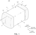
- FIG. 1 schematically illustrates a perspective view of a multilayer electronic component according to an embodiment.
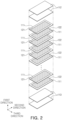
- FIG. 2 is a schematic illustration of an exploded perspective view illustrating a stacked structure of an internal electrode.
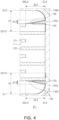
- FIG. 4 is a schematic illustration of an enlarged view of a P1 region of FIG. 3 .
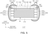
- FIG. 5 is a schematic illustration of a cross-sectional view taken along line I-I' of a multilayer electronic component according to another embodiment.
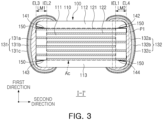
- a multilayer electronic component 100 includes a body 110 including a capacitance formation portion Ac including a dielectric layer 111 and internal electrodes 121 and 122 alternately stacked with the dielectric layer 111, and cover portions 112 and 113 disposed on both end surfaces of the capacitance formation portion Ac in the stacking direction; and external electrodes 131 and 132 disposed on the body 110.
- a capacitance formation portion Ac including a dielectric layer 111 and internal electrodes 121 and 122 alternately stacked with the dielectric layer 111, and cover portions 112 and 113 disposed on both end surfaces of the capacitance formation portion Ac in the stacking direction; and external electrodes 131 and 132 disposed on the body 110.
- the body 110 may have a dielectric layer 111 and internal electrodes 121 and 122 alternately stacked.
- the body 110 may have a hexahedral shape or a shape similar thereto. Due to shrinkage of the ceramic particles included in the body 110 during firing, the body 110 may have a substantially hexahedral shape, although it does not have a perfectly straight hexahedral shape.
- the body 110 may have first and second surfaces 1 and 2 opposing each other in a first direction, third and fourth surfaces 3 and 4 connected to the first and second surfaces 1 and 2 and opposing each other in a second direction, and fifth and sixth surfaces 5 and 6 connected to the first to fourth surfaces 1, 2, 3 and 4 and opposing each other in the third direction.
- the plurality of dielectric layers 111 forming the body 110 are in a fired state, and the boundary between adjacent dielectric layers 111 will be unified to the extent that it is difficult to confirm without using a scanning electron microscope (SEM).
- SEM scanning electron microscope
- the raw material forming the dielectric layer 111 is not limited as long as sufficient capacitance may be obtained.
- a perovskite (ABO 3 )-based material may be used, and for example, a barium titanate-based material, a lead composite perovskite-based material, a strontium titanate-based material or the like may be used.
- the barium titanate-based material may include BaTiO 3 -based ceramic particles.
- the ceramic particles BaTiO 3 , or (Ba 1-x Ca x )TiO 3 (0 ⁇ x ⁇ 1, Ba(Ti 1-y Ca y )O 3 (0 ⁇ y ⁇ 1, (Ba 1-x Ca x ) (Ti 1-y Zr y )O 3 (0 ⁇ x ⁇ 1, 0 ⁇ y ⁇ 1 or Ba(Ti 1-y Zr y )O 3 (0 ⁇ y ⁇ 1 in which calcium (Ca), zirconium (Zr) or the like is partially solid-solubilized in BaTiO 3 , may be provided.
- various ceramic additives, organic solvents, binders, dispersants, and the like may be added to powder such as barium titanate (BaTiO 3 ), as a raw material forming the dielectric layer 111 according to the usage of the present disclosure.
- barium titanate BaTiO 3
- the thickness of the dielectric layer 111 does not need to be specifically limited.
- the thickness of the dielectric layer 111 may refer to the thickness of the dielectric layer 111 disposed between the first and second internal electrodes 121 and 122.
- the thickness of the dielectric layer 111 may refer to the size of the dielectric layer 111 in the first direction.
- the thickness of the dielectric layer 111 may refer to the average thickness of the dielectric layer 111 and may refer to the average size of the dielectric layer 111 in the first direction.
- first internal electrode 121 may be spaced apart from the fourth surface 4 and exposed through the third surface 3
- second internal electrode 122 may be spaced apart from the third surface 3 and exposed through the fourth surface 4.
- a first external electrode 131 is disposed on the third surface 3 of the body 110 and connected to the first internal electrode 121
- a second external electrode 132 is disposed on the fourth surface 4 of the body 110 and connected to the second internal electrode 122.
- the type of the plating layers 131c and 132c is not particularly limited, and may be a single layer of the plating layers 131c and 132c including at least one of nickel (Ni), tin (Sn), silver (Ag), palladium (Pd), or alloys thereof, or may be formed of multiple layers.
- the plating layers 131c and 132c may be a Ni plating layer or a Sn plating layer, and may be in a form in which a Ni plating layer and a Sn plating layer are sequentially formed on an electrode layer, or may be in a form in which a Sn plating layer, a Ni plating layer, and a Sn plating layer are sequentially formed.
- the plating layers 131c and 132c may include multiple Ni plating layers and/or multiple Sn plating layers.
- the lead-in portions 141, 142, 143 and 144 may include first and second lead-in portions 141 and 142 disposed between the capacitance formation portion Ac and the first cover portion 112, and third and fourth lead-in portions 143 and 144 disposed between the capacitance formation portion Ac and the second cover portion 113.
- the first and third lead-in portions 141 and 143 may be disposed in positions adjacent to the third surface 3, and the second and fourth lead-in portions 142 and 144 may be disposed in positions adjacent to the fourth surface 4.
- the lead-in portions 141, 142, 143 and 144 are illustrated as being formed in all four regions, which are interfaces between the capacitance formation portion Ac and the cover portions 112 and 113, but they are not particularly limited thereto, and even if they are formed in at least one region among the four regions, the moisture resistance reliability of the multilayer electronic component 100 may be improved.
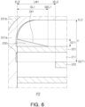
- FIG. 5 which schematically illustrates a multilayer electronic component 200 according to another embodiment, it may be confirmed that the lead-in portions 241 and 242 are formed in two areas between the capacitance formation portion Ac and the first cover portion 212.
- the lead-in portions 141, 142, 143 and 144 may be disposed only between the capacitance formation portion Ac and the cover portions 112 and 113.
- At least a portion of the glass 150 included in the lead-in portions 141, 142, 143 and 144 may be disposed to be in contact with at least one of the cover portions 112 and 113 and the capacitance formation portion Ac.
- the glass 150 may be disposed to be in contact with at least a portion of the cover portions 112 and 113 corresponding to a portion of the surface of the body 110, and at least a portion of the capacitance formation portion Ac.
- the thickness of the glass 150 disposed to be in contact with at least one of the cover portions 112 and 113 and the capacitance formation portion Ac may be 0.1 um or more.
- the thickness of the glass 150 is 0.1 um or more, it may effectively suppress external moisture penetration and improve the moisture resistance reliability of the multilayer electronic component 100, and the upper limit of the thickness is not particularly limited, and as described below, the glass may fill the lead-in portion.
- the lead-in portions 241 and 242 may be filled with glass 250.
- the drawing illustrates that the first and second lead-in portions 241 and 242 are formed only between the capacitance formation portion Ac and the first cover portion 212, and the glass 250 fills the first and second lead-in portions 241 and 242, but the present disclosure is not particularly limited thereto, and the lead-in portions may also be formed between the capacitance formation portion Ac and the second cover portion 213 and filled with glass.
- the glass 150 may be further disposed in a layer shape on the surface of the body 110.
Landscapes
- Engineering & Computer Science (AREA)
- Power Engineering (AREA)
- Manufacturing & Machinery (AREA)
- Microelectronics & Electronic Packaging (AREA)
- Ceramic Engineering (AREA)
- Chemical & Material Sciences (AREA)
- Inorganic Chemistry (AREA)
- Fixed Capacitors And Capacitor Manufacturing Machines (AREA)
- Ceramic Capacitors (AREA)
Applications Claiming Priority (1)
| Application Number | Priority Date | Filing Date | Title |
|---|---|---|---|
| KR1020230196825A KR20250104438A (ko) | 2023-12-29 | 2023-12-29 | 적층형 전자 부품 |
Publications (1)
| Publication Number | Publication Date |
|---|---|
| EP4579705A1 true EP4579705A1 (de) | 2025-07-02 |
Family
ID=93841831
Family Applications (1)
| Application Number | Title | Priority Date | Filing Date |
|---|---|---|---|
| EP24218112.1A Pending EP4579705A1 (de) | 2023-12-29 | 2024-12-06 | Mehrschichtiges elektronisches bauteil |
Country Status (5)
| Country | Link |
|---|---|
| US (1) | US20250218672A1 (de) |
| EP (1) | EP4579705A1 (de) |
| JP (1) | JP2025105502A (de) |
| KR (1) | KR20250104438A (de) |
| CN (1) | CN120236898A (de) |
Citations (5)
| Publication number | Priority date | Publication date | Assignee | Title |
|---|---|---|---|---|
| US20130294010A1 (en) * | 2012-05-03 | 2013-11-07 | Samsung Electro-Mechanics Co., Ltd. | Multilayer ceramic electronic component and method of manufacturing the same |
| US11239032B2 (en) * | 2019-07-08 | 2022-02-01 | Samsung Electro-Mechanics Co., Ltd. | Capacitor component |
| US20220199331A1 (en) * | 2020-12-18 | 2022-06-23 | Samsung Electro-Mechanics Co., Ltd. | Electronic component and method of manufacturing the same |
| US11410814B2 (en) * | 2020-09-04 | 2022-08-09 | Samsung Electro-Mechanics Co., Ltd. | Multilayer electronic component |
| US20230260700A1 (en) * | 2022-02-15 | 2023-08-17 | Murata Manufacturing Co., Ltd. | Multilayer ceramic electronic component |
Family Cites Families (1)
| Publication number | Priority date | Publication date | Assignee | Title |
|---|---|---|---|---|
| KR102333093B1 (ko) | 2019-07-08 | 2021-12-01 | 삼성전기주식회사 | 커패시터 부품 |
-
2023
- 2023-12-29 KR KR1020230196825A patent/KR20250104438A/ko active Pending
-
2024
- 2024-12-06 EP EP24218112.1A patent/EP4579705A1/de active Pending
- 2024-12-06 US US18/972,242 patent/US20250218672A1/en active Pending
- 2024-12-10 JP JP2024215100A patent/JP2025105502A/ja active Pending
- 2024-12-27 CN CN202411947425.3A patent/CN120236898A/zh active Pending
Patent Citations (5)
| Publication number | Priority date | Publication date | Assignee | Title |
|---|---|---|---|---|
| US20130294010A1 (en) * | 2012-05-03 | 2013-11-07 | Samsung Electro-Mechanics Co., Ltd. | Multilayer ceramic electronic component and method of manufacturing the same |
| US11239032B2 (en) * | 2019-07-08 | 2022-02-01 | Samsung Electro-Mechanics Co., Ltd. | Capacitor component |
| US11410814B2 (en) * | 2020-09-04 | 2022-08-09 | Samsung Electro-Mechanics Co., Ltd. | Multilayer electronic component |
| US20220199331A1 (en) * | 2020-12-18 | 2022-06-23 | Samsung Electro-Mechanics Co., Ltd. | Electronic component and method of manufacturing the same |
| US20230260700A1 (en) * | 2022-02-15 | 2023-08-17 | Murata Manufacturing Co., Ltd. | Multilayer ceramic electronic component |
Also Published As
| Publication number | Publication date |
|---|---|
| CN120236898A (zh) | 2025-07-01 |
| KR20250104438A (ko) | 2025-07-08 |
| JP2025105502A (ja) | 2025-07-10 |
| US20250218672A1 (en) | 2025-07-03 |
Similar Documents
| Publication | Publication Date | Title |
|---|---|---|
| CN114551098A (zh) | 多层电子组件 | |
| EP4542598A1 (de) | Mehrschichtiges elektronisches bauteil | |
| EP4401104A2 (de) | Mehrschichtiges elektronisches bauteil | |
| US12136518B2 (en) | Multilayer electronic component including cover layer having insulating and conductive portions | |
| EP4579705A1 (de) | Mehrschichtiges elektronisches bauteil | |
| US20240062966A1 (en) | Multilayer electronic component | |
| KR20250075162A (ko) | 적층형 전자 부품 | |
| US12176153B2 (en) | Multilayer electronic component | |
| KR102900301B1 (ko) | 적층형 전자 부품 | |
| CN111009415A (zh) | 陶瓷电子组件 | |
| US20250218690A1 (en) | Multilayer electronic component | |
| US20250166914A1 (en) | Multilayer electronic component | |
| US20250054702A1 (en) | Multilayered electronic component | |
| EP4539069A2 (de) | Leitfähige harzzwischenschicht für eine externe elektrode eines mehrschichtigen keramischen bauteils mit metallteilchen und kern-schalen-teilchen (kern: harz; schale: metall) in einer polymermatrix | |
| EP4560660A1 (de) | Mehrschichtiges elektronisches bauteil | |
| US20230238182A1 (en) | Multilayer electronic component | |
| EP4546382A2 (de) | Diskontinuierliche grenzflächenschicht für ein mehrschichtiges keramikbauteil mit einem an aluminium-nickel-legierung reichen bereich, der mit den inneren nickelelektroden in kontakt steht, und einem an kupfer-aluminium-legierung reichen bereich, der mit den äusseren kupferelektroden in kontakt steht | |
| EP4394826A2 (de) | Mehrschichtiges elektronisches bauteil | |
| US20250125097A1 (en) | Multilayer electronic component | |
| EP4415012A1 (de) | Mehrschichtiges elektronisches bauteil | |
| KR20250072023A (ko) | 적층형 전자 부품 | |
| KR20250080379A (ko) | 적층형 전자 부품 | |
| KR20250096047A (ko) | 적층형 전자 부품 | |
| KR20240129782A (ko) | 적층형 전자 부품 | |
| KR20250071663A (ko) | 적층형 전자 부품 |
Legal Events
| Date | Code | Title | Description |
|---|---|---|---|
| PUAI | Public reference made under article 153(3) epc to a published international application that has entered the european phase |
Free format text: ORIGINAL CODE: 0009012 |
|
| STAA | Information on the status of an ep patent application or granted ep patent |
Free format text: STATUS: THE APPLICATION HAS BEEN PUBLISHED |
|
| AK | Designated contracting states |
Kind code of ref document: A1 Designated state(s): AL AT BE BG CH CY CZ DE DK EE ES FI FR GB GR HR HU IE IS IT LI LT LU LV MC ME MK MT NL NO PL PT RO RS SE SI SK SM TR |
|
| STAA | Information on the status of an ep patent application or granted ep patent |
Free format text: STATUS: REQUEST FOR EXAMINATION WAS MADE |
|
| 17P | Request for examination filed |
Effective date: 20250926 |