EP4394826A2 - Mehrschichtiges elektronisches bauteil - Google Patents
Mehrschichtiges elektronisches bauteil Download PDFInfo
- Publication number
- EP4394826A2 EP4394826A2 EP23216218.0A EP23216218A EP4394826A2 EP 4394826 A2 EP4394826 A2 EP 4394826A2 EP 23216218 A EP23216218 A EP 23216218A EP 4394826 A2 EP4394826 A2 EP 4394826A2
- Authority
- EP
- European Patent Office
- Prior art keywords
- core
- core portion
- dielectric
- electronic component
- multilayer electronic
- Prior art date
- Legal status (The legal status is an assumption and is not a legal conclusion. Google has not performed a legal analysis and makes no representation as to the accuracy of the status listed.)
- Pending
Links
Images


Classifications
-
- H—ELECTRICITY
- H01—ELECTRIC ELEMENTS
- H01G—CAPACITORS; CAPACITORS, RECTIFIERS, DETECTORS, SWITCHING DEVICES, LIGHT-SENSITIVE OR TEMPERATURE-SENSITIVE DEVICES OF THE ELECTROLYTIC TYPE
- H01G4/00—Fixed capacitors; Processes of their manufacture
- H01G4/002—Details
- H01G4/018—Dielectrics
- H01G4/06—Solid dielectrics
- H01G4/08—Inorganic dielectrics
- H01G4/12—Ceramic dielectrics
- H01G4/1209—Ceramic dielectrics characterised by the ceramic dielectric material
- H01G4/1218—Ceramic dielectrics characterised by the ceramic dielectric material based on titanium oxides or titanates
-
- C—CHEMISTRY; METALLURGY
- C04—CEMENTS; CONCRETE; ARTIFICIAL STONE; CERAMICS; REFRACTORIES
- C04B—LIME, MAGNESIA; SLAG; CEMENTS; COMPOSITIONS THEREOF, e.g. MORTARS, CONCRETE OR LIKE BUILDING MATERIALS; ARTIFICIAL STONE; CERAMICS; REFRACTORIES; TREATMENT OF NATURAL STONE
- C04B35/00—Shaped ceramic products characterised by their composition; Ceramics compositions; Processing powders of inorganic compounds preparatory to the manufacturing of ceramic products
- C04B35/01—Shaped ceramic products characterised by their composition; Ceramics compositions; Processing powders of inorganic compounds preparatory to the manufacturing of ceramic products based on oxide ceramics
- C04B35/46—Shaped ceramic products characterised by their composition; Ceramics compositions; Processing powders of inorganic compounds preparatory to the manufacturing of ceramic products based on oxide ceramics based on titanium oxides or titanates
- C04B35/462—Shaped ceramic products characterised by their composition; Ceramics compositions; Processing powders of inorganic compounds preparatory to the manufacturing of ceramic products based on oxide ceramics based on titanium oxides or titanates based on titanates
- C04B35/465—Shaped ceramic products characterised by their composition; Ceramics compositions; Processing powders of inorganic compounds preparatory to the manufacturing of ceramic products based on oxide ceramics based on titanium oxides or titanates based on titanates based on alkaline earth metal titanates
- C04B35/468—Shaped ceramic products characterised by their composition; Ceramics compositions; Processing powders of inorganic compounds preparatory to the manufacturing of ceramic products based on oxide ceramics based on titanium oxides or titanates based on titanates based on alkaline earth metal titanates based on barium titanates
- C04B35/4682—Shaped ceramic products characterised by their composition; Ceramics compositions; Processing powders of inorganic compounds preparatory to the manufacturing of ceramic products based on oxide ceramics based on titanium oxides or titanates based on titanates based on alkaline earth metal titanates based on barium titanates based on BaTiO3 perovskite phase
-
- C—CHEMISTRY; METALLURGY
- C04—CEMENTS; CONCRETE; ARTIFICIAL STONE; CERAMICS; REFRACTORIES
- C04B—LIME, MAGNESIA; SLAG; CEMENTS; COMPOSITIONS THEREOF, e.g. MORTARS, CONCRETE OR LIKE BUILDING MATERIALS; ARTIFICIAL STONE; CERAMICS; REFRACTORIES; TREATMENT OF NATURAL STONE
- C04B35/00—Shaped ceramic products characterised by their composition; Ceramics compositions; Processing powders of inorganic compounds preparatory to the manufacturing of ceramic products
- C04B35/01—Shaped ceramic products characterised by their composition; Ceramics compositions; Processing powders of inorganic compounds preparatory to the manufacturing of ceramic products based on oxide ceramics
- C04B35/46—Shaped ceramic products characterised by their composition; Ceramics compositions; Processing powders of inorganic compounds preparatory to the manufacturing of ceramic products based on oxide ceramics based on titanium oxides or titanates
- C04B35/462—Shaped ceramic products characterised by their composition; Ceramics compositions; Processing powders of inorganic compounds preparatory to the manufacturing of ceramic products based on oxide ceramics based on titanium oxides or titanates based on titanates
- C04B35/465—Shaped ceramic products characterised by their composition; Ceramics compositions; Processing powders of inorganic compounds preparatory to the manufacturing of ceramic products based on oxide ceramics based on titanium oxides or titanates based on titanates based on alkaline earth metal titanates
- C04B35/47—Shaped ceramic products characterised by their composition; Ceramics compositions; Processing powders of inorganic compounds preparatory to the manufacturing of ceramic products based on oxide ceramics based on titanium oxides or titanates based on titanates based on alkaline earth metal titanates based on strontium titanates
-
- C—CHEMISTRY; METALLURGY
- C04—CEMENTS; CONCRETE; ARTIFICIAL STONE; CERAMICS; REFRACTORIES
- C04B—LIME, MAGNESIA; SLAG; CEMENTS; COMPOSITIONS THEREOF, e.g. MORTARS, CONCRETE OR LIKE BUILDING MATERIALS; ARTIFICIAL STONE; CERAMICS; REFRACTORIES; TREATMENT OF NATURAL STONE
- C04B35/00—Shaped ceramic products characterised by their composition; Ceramics compositions; Processing powders of inorganic compounds preparatory to the manufacturing of ceramic products
- C04B35/01—Shaped ceramic products characterised by their composition; Ceramics compositions; Processing powders of inorganic compounds preparatory to the manufacturing of ceramic products based on oxide ceramics
- C04B35/48—Shaped ceramic products characterised by their composition; Ceramics compositions; Processing powders of inorganic compounds preparatory to the manufacturing of ceramic products based on oxide ceramics based on zirconium or hafnium oxides, zirconates, zircon or hafnates
- C04B35/49—Shaped ceramic products characterised by their composition; Ceramics compositions; Processing powders of inorganic compounds preparatory to the manufacturing of ceramic products based on oxide ceramics based on zirconium or hafnium oxides, zirconates, zircon or hafnates containing also titanium oxides or titanates
-
- C—CHEMISTRY; METALLURGY
- C04—CEMENTS; CONCRETE; ARTIFICIAL STONE; CERAMICS; REFRACTORIES
- C04B—LIME, MAGNESIA; SLAG; CEMENTS; COMPOSITIONS THEREOF, e.g. MORTARS, CONCRETE OR LIKE BUILDING MATERIALS; ARTIFICIAL STONE; CERAMICS; REFRACTORIES; TREATMENT OF NATURAL STONE
- C04B35/00—Shaped ceramic products characterised by their composition; Ceramics compositions; Processing powders of inorganic compounds preparatory to the manufacturing of ceramic products
- C04B35/622—Forming processes; Processing powders of inorganic compounds preparatory to the manufacturing of ceramic products
- C04B35/626—Preparing or treating the powders individually or as batches ; preparing or treating macroscopic reinforcing agents for ceramic products, e.g. fibres; mechanical aspects section B
- C04B35/628—Coating the powders or the macroscopic reinforcing agents
- C04B35/62802—Powder coating materials
- C04B35/62805—Oxide ceramics
- C04B35/62815—Rare earth metal oxides
-
- C—CHEMISTRY; METALLURGY
- C04—CEMENTS; CONCRETE; ARTIFICIAL STONE; CERAMICS; REFRACTORIES
- C04B—LIME, MAGNESIA; SLAG; CEMENTS; COMPOSITIONS THEREOF, e.g. MORTARS, CONCRETE OR LIKE BUILDING MATERIALS; ARTIFICIAL STONE; CERAMICS; REFRACTORIES; TREATMENT OF NATURAL STONE
- C04B35/00—Shaped ceramic products characterised by their composition; Ceramics compositions; Processing powders of inorganic compounds preparatory to the manufacturing of ceramic products
- C04B35/622—Forming processes; Processing powders of inorganic compounds preparatory to the manufacturing of ceramic products
- C04B35/626—Preparing or treating the powders individually or as batches ; preparing or treating macroscopic reinforcing agents for ceramic products, e.g. fibres; mechanical aspects section B
- C04B35/628—Coating the powders or the macroscopic reinforcing agents
- C04B35/62802—Powder coating materials
- C04B35/62805—Oxide ceramics
- C04B35/62818—Refractory metal oxides
- C04B35/62823—Zirconium or hafnium oxide
-
- C—CHEMISTRY; METALLURGY
- C04—CEMENTS; CONCRETE; ARTIFICIAL STONE; CERAMICS; REFRACTORIES
- C04B—LIME, MAGNESIA; SLAG; CEMENTS; COMPOSITIONS THEREOF, e.g. MORTARS, CONCRETE OR LIKE BUILDING MATERIALS; ARTIFICIAL STONE; CERAMICS; REFRACTORIES; TREATMENT OF NATURAL STONE
- C04B35/00—Shaped ceramic products characterised by their composition; Ceramics compositions; Processing powders of inorganic compounds preparatory to the manufacturing of ceramic products
- C04B35/622—Forming processes; Processing powders of inorganic compounds preparatory to the manufacturing of ceramic products
- C04B35/626—Preparing or treating the powders individually or as batches ; preparing or treating macroscopic reinforcing agents for ceramic products, e.g. fibres; mechanical aspects section B
- C04B35/628—Coating the powders or the macroscopic reinforcing agents
- C04B35/62894—Coating the powders or the macroscopic reinforcing agents with more than one coating layer
-
- C—CHEMISTRY; METALLURGY
- C04—CEMENTS; CONCRETE; ARTIFICIAL STONE; CERAMICS; REFRACTORIES
- C04B—LIME, MAGNESIA; SLAG; CEMENTS; COMPOSITIONS THEREOF, e.g. MORTARS, CONCRETE OR LIKE BUILDING MATERIALS; ARTIFICIAL STONE; CERAMICS; REFRACTORIES; TREATMENT OF NATURAL STONE
- C04B35/00—Shaped ceramic products characterised by their composition; Ceramics compositions; Processing powders of inorganic compounds preparatory to the manufacturing of ceramic products
- C04B35/622—Forming processes; Processing powders of inorganic compounds preparatory to the manufacturing of ceramic products
- C04B35/626—Preparing or treating the powders individually or as batches ; preparing or treating macroscopic reinforcing agents for ceramic products, e.g. fibres; mechanical aspects section B
- C04B35/628—Coating the powders or the macroscopic reinforcing agents
- C04B35/62897—Coatings characterised by their thickness
-
- H—ELECTRICITY
- H01—ELECTRIC ELEMENTS
- H01G—CAPACITORS; CAPACITORS, RECTIFIERS, DETECTORS, SWITCHING DEVICES, LIGHT-SENSITIVE OR TEMPERATURE-SENSITIVE DEVICES OF THE ELECTROLYTIC TYPE
- H01G4/00—Fixed capacitors; Processes of their manufacture
- H01G4/002—Details
- H01G4/005—Electrodes
- H01G4/012—Form of non-self-supporting electrodes
-
- H—ELECTRICITY
- H01—ELECTRIC ELEMENTS
- H01G—CAPACITORS; CAPACITORS, RECTIFIERS, DETECTORS, SWITCHING DEVICES, LIGHT-SENSITIVE OR TEMPERATURE-SENSITIVE DEVICES OF THE ELECTROLYTIC TYPE
- H01G4/00—Fixed capacitors; Processes of their manufacture
- H01G4/002—Details
- H01G4/018—Dielectrics
- H01G4/06—Solid dielectrics
- H01G4/08—Inorganic dielectrics
- H01G4/12—Ceramic dielectrics
- H01G4/1209—Ceramic dielectrics characterised by the ceramic dielectric material
- H01G4/1218—Ceramic dielectrics characterised by the ceramic dielectric material based on titanium oxides or titanates
- H01G4/1227—Ceramic dielectrics characterised by the ceramic dielectric material based on titanium oxides or titanates based on alkaline earth titanates
-
- H—ELECTRICITY
- H01—ELECTRIC ELEMENTS
- H01G—CAPACITORS; CAPACITORS, RECTIFIERS, DETECTORS, SWITCHING DEVICES, LIGHT-SENSITIVE OR TEMPERATURE-SENSITIVE DEVICES OF THE ELECTROLYTIC TYPE
- H01G4/00—Fixed capacitors; Processes of their manufacture
- H01G4/002—Details
- H01G4/228—Terminals
- H01G4/232—Terminals electrically connecting two or more layers of a stacked or rolled capacitor
- H01G4/2325—Terminals electrically connecting two or more layers of a stacked or rolled capacitor characterised by the material of the terminals
-
- H—ELECTRICITY
- H01—ELECTRIC ELEMENTS
- H01G—CAPACITORS; CAPACITORS, RECTIFIERS, DETECTORS, SWITCHING DEVICES, LIGHT-SENSITIVE OR TEMPERATURE-SENSITIVE DEVICES OF THE ELECTROLYTIC TYPE
- H01G4/00—Fixed capacitors; Processes of their manufacture
- H01G4/30—Stacked capacitors
-
- C—CHEMISTRY; METALLURGY
- C04—CEMENTS; CONCRETE; ARTIFICIAL STONE; CERAMICS; REFRACTORIES
- C04B—LIME, MAGNESIA; SLAG; CEMENTS; COMPOSITIONS THEREOF, e.g. MORTARS, CONCRETE OR LIKE BUILDING MATERIALS; ARTIFICIAL STONE; CERAMICS; REFRACTORIES; TREATMENT OF NATURAL STONE
- C04B2235/00—Aspects relating to ceramic starting mixtures or sintered ceramic products
- C04B2235/02—Composition of constituents of the starting material or of secondary phases of the final product
- C04B2235/30—Constituents and secondary phases not being of a fibrous nature
- C04B2235/32—Metal oxides, mixed metal oxides, or oxide-forming salts thereof, e.g. carbonates, nitrates, (oxy)hydroxides, chlorides
- C04B2235/3205—Alkaline earth oxides or oxide forming salts thereof, e.g. beryllium oxide
- C04B2235/3208—Calcium oxide or oxide-forming salts thereof, e.g. lime
-
- C—CHEMISTRY; METALLURGY
- C04—CEMENTS; CONCRETE; ARTIFICIAL STONE; CERAMICS; REFRACTORIES
- C04B—LIME, MAGNESIA; SLAG; CEMENTS; COMPOSITIONS THEREOF, e.g. MORTARS, CONCRETE OR LIKE BUILDING MATERIALS; ARTIFICIAL STONE; CERAMICS; REFRACTORIES; TREATMENT OF NATURAL STONE
- C04B2235/00—Aspects relating to ceramic starting mixtures or sintered ceramic products
- C04B2235/02—Composition of constituents of the starting material or of secondary phases of the final product
- C04B2235/30—Constituents and secondary phases not being of a fibrous nature
- C04B2235/32—Metal oxides, mixed metal oxides, or oxide-forming salts thereof, e.g. carbonates, nitrates, (oxy)hydroxides, chlorides
- C04B2235/3205—Alkaline earth oxides or oxide forming salts thereof, e.g. beryllium oxide
- C04B2235/3215—Barium oxides or oxide-forming salts thereof
-
- C—CHEMISTRY; METALLURGY
- C04—CEMENTS; CONCRETE; ARTIFICIAL STONE; CERAMICS; REFRACTORIES
- C04B—LIME, MAGNESIA; SLAG; CEMENTS; COMPOSITIONS THEREOF, e.g. MORTARS, CONCRETE OR LIKE BUILDING MATERIALS; ARTIFICIAL STONE; CERAMICS; REFRACTORIES; TREATMENT OF NATURAL STONE
- C04B2235/00—Aspects relating to ceramic starting mixtures or sintered ceramic products
- C04B2235/70—Aspects relating to sintered or melt-casted ceramic products
- C04B2235/74—Physical characteristics
- C04B2235/76—Crystal structural characteristics, e.g. symmetry
- C04B2235/768—Perovskite structure ABO3
-
- C—CHEMISTRY; METALLURGY
- C04—CEMENTS; CONCRETE; ARTIFICIAL STONE; CERAMICS; REFRACTORIES
- C04B—LIME, MAGNESIA; SLAG; CEMENTS; COMPOSITIONS THEREOF, e.g. MORTARS, CONCRETE OR LIKE BUILDING MATERIALS; ARTIFICIAL STONE; CERAMICS; REFRACTORIES; TREATMENT OF NATURAL STONE
- C04B2235/00—Aspects relating to ceramic starting mixtures or sintered ceramic products
- C04B2235/70—Aspects relating to sintered or melt-casted ceramic products
- C04B2235/74—Physical characteristics
- C04B2235/78—Grain sizes and shapes, product microstructures, e.g. acicular grains, equiaxed grains, platelet-structures
- C04B2235/785—Submicron sized grains, i.e. from 0,1 to 1 micron
-
- C—CHEMISTRY; METALLURGY
- C04—CEMENTS; CONCRETE; ARTIFICIAL STONE; CERAMICS; REFRACTORIES
- C04B—LIME, MAGNESIA; SLAG; CEMENTS; COMPOSITIONS THEREOF, e.g. MORTARS, CONCRETE OR LIKE BUILDING MATERIALS; ARTIFICIAL STONE; CERAMICS; REFRACTORIES; TREATMENT OF NATURAL STONE
- C04B2235/00—Aspects relating to ceramic starting mixtures or sintered ceramic products
- C04B2235/70—Aspects relating to sintered or melt-casted ceramic products
- C04B2235/80—Phases present in the sintered or melt-cast ceramic products other than the main phase
- C04B2235/85—Intergranular or grain boundary phases
-
- H—ELECTRICITY
- H01—ELECTRIC ELEMENTS
- H01G—CAPACITORS; CAPACITORS, RECTIFIERS, DETECTORS, SWITCHING DEVICES, LIGHT-SENSITIVE OR TEMPERATURE-SENSITIVE DEVICES OF THE ELECTROLYTIC TYPE
- H01G4/00—Fixed capacitors; Processes of their manufacture
- H01G4/002—Details
- H01G4/018—Dielectrics
- H01G4/06—Solid dielectrics
- H01G4/08—Inorganic dielectrics
- H01G4/12—Ceramic dielectrics
- H01G4/1209—Ceramic dielectrics characterised by the ceramic dielectric material
Definitions
- a multilayer electronic component may be a chip condenser mounted on a printed circuit board of various types of electronic products such as imaging devices including a liquid crystal display (LCD) and a plasma display panel (PDP), a computer, a smartphone, and a mobile phone and charging or discharging electricity.
- imaging devices including a liquid crystal display (LCD) and a plasma display panel (PDP), a computer, a smartphone, and a mobile phone and charging or discharging electricity.
- LCD liquid crystal display
- PDP plasma display panel
- a multilayer electronic component includes a body including a dielectric layer and an internal electrode; and external electrodes disposed on the body.
- the dielectric layer includes a plurality of dielectric grains having a perovskite-based composition represented by ABO 3 , the A includes a first element including at least one of Bi, Na, K, Sr, and Ca, and the B includes a second element including Ti.
- At least one of the plurality of dielectric grains has a core-shell structure including a core portion on an internal side and a shell portion covering at least a portion of the core portion, and a content of the first element included in the core portion is twice or more than a content of the first element included in the shell portion.
- the core portion includes a first core portion on an internal side and a second core portion covering at least a portion of the first core portion, and the second core portion includes Zr.
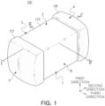
- a first direction may be defined as a lamination direction or a thickness T direction
- a second direction may be defined as a length L direction
- a third direction may be defined as a width W direction.
- FIG. 1 is a perspective diagram illustrating a multilayer electronic component according to an example embodiment.
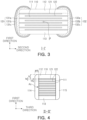
- FIG. 2 is an exploded perspective diagram illustrating a laminate structure of internal electrodes according to an example embodiment.
- FIG. 3 is a cross-sectional diagram taken along line I-I' in FIG. 1 .
- FIG. 4 is a cross-sectional diagram taken along line II-II' in FIG. 1 .
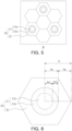
- FIG. 5 is an enlarged diagram illustrating region P in FIG. 3 .
- FIG. 6 is a diagram illustrating a dielectric grain having a core-shell structure according to an example embodiment.
- FIG. 7 is a diagram illustrating a dielectric grain having a core-shell structure according to an example embodiment.
- FIG. 8 is a diagram illustrating an element content (mass percentage) for each region of a dielectric grain having a core-shell structure according to an example embodiment.
- a multilayer electronic component according to an example embodiment will be described in greater detail with reference to FIGS. 1 to 8 .
- a multilayer ceramic capacitor will be described as an example of a multilayer electronic component, but the example embodiment may also be applied to various electronic products using a dielectric composition, such as an inductor, a piezoelectric element, a varistor, or a thermistor.
- a multilayer electronic component 100 may include a body 110 including a dielectric layer 111 and internal electrodes 121 and 122; and external electrodes 131 and 132 disposed on the body 110.
- the dielectric layer 111 may include a plurality of dielectric grains having a perovskite-based composition represented by ABO 3
- the A may include a first element including at least one of Bi, Na, K, Sr, and Ca
- the B may include a second element including Ti
- at least one of the plurality of dielectric grains may include a core-shell structure 20 including a core portion 21 on an internal side and a shell portion 22 covering at least a portion of the core portion 21, the content of the first element included in the core portion 21 may be twice or more than the content of the first element included in the shell portion 22,
- the core portion 21 may include a first core portion 21a on an internal side and a second core portion 21b covering at least a portion of the first core portion 21a
- the second core portion 21b may include Zr.
- the dielectric layers 111 and internal electrodes 121 and 122 may be alternately laminated.
- the body 110 may have first and second surfaces 1 and 2 opposing each other in the first direction, third and fourth surfaces 3 and 4 connected to the first and second surfaces 1 and 2 and opposing in the second direction, and fifth and sixth surfaces 5 and 6 connected to the first and second surfaces 1 and 2 and the third and fourth surfaces 3 and 4 and opposing each other in the third direction.
- the plurality of dielectric layers 111 forming the body 110 may be in a sintered state, and a boundary between the adjacent dielectric layers 111 may be integrated with each other such that the boundary may not be distinct without using a scanning electron microscope (SEM).
- SEM scanning electron microscope
- the barium titanate material may include BaTiO 3 ceramic powder, and an example of the ceramic powder may include (Ba 1-x Ca x )TiO 3 (0 ⁇ x ⁇ 1), Ba(Ti 1-y Ca y )O 3 (0 ⁇ y ⁇ 1), (Ba 1-x Ca x )(Ti 1-y Zr y )O 3 (0 ⁇ x ⁇ 1, 0 ⁇ y ⁇ 1) or Ba(Ti 1-y Zr y )O 3 (0 ⁇ y ⁇ 1) in which Ca (calcium), Zr (zirconium) is partially solid-solute.
- various ceramic additives, organic solvents, binders, dispersants, or the like may be added to a raw material for forming the dielectric layer 111 in the example embodiment to powder such as barium titanate (BaTiO 3 ).
- the A-site in the ABO 3 perovskite-based composition may include a first element including at least one of Bi, Na, K, Sr, and Ca.
- the B-site may include a second element including Ti, but an example embodiment thereof is not limited thereto, and may include at least one element of Hf and Zr.
- the A-site of the ABO 3 perovskite-based composition may include a first element including at least one of Bi, Na, K, Sr, and Ca, and the B-site may include a second element including at least one of Ti, Hf, and Zr, such that degradation of dielectric properties due to DC-bias properties may be effectively prevented even under high-temperature/high-voltage conditions, thereby manufacturing a multilayer electronic component having improved reliability.
- the content of the first element may be 80 mol% or more based on 100 mol% of the A-site element
- the content of the second element may be 80 mol% or more based on 100 mol% of the B-site element.
- Dc-bias properties may be improved, and by including 80 mol% or more of the second element based on 100 mol% of the B element, the effect of improvement in reliability may be excellent.
- an average value may be calculated by measuring 5 or more points on the core portion 21 and 10 or more points on the shell portion 22, and the first element content of the entirety of pixels may be measured by mapping the first element, and the content of the first element included in each region may be calculated from the first element content of the entirety of pixels.
- the effect of improvement of the Dc-bias properties may decrease, but when the fraction of the shell portion 22 is determined to be low, it may be difficult to form a uniform and stable shell portion 22, such that it may be difficult to expect the effect of improvement in dielectric properties to be supplemented, particularly the effect of improvement in reliability.
- insulation resistance may be increased, and the fraction of the shell portion 22 may be stably reduced and may be formed uniformly, such that dielectric properties may be supplemented while improving insulation resistance properties.
- the method of forming the zirconium (Zr) substitution layer is not limited to any particular example, and by coating and pre-diffusing zirconium (Zr) on the ABO 3 base material powder before sintering, zirconium (Zr) may be diffused into the core portion 21, and a second core portion 21b including zirconium (Zr) in the dielectric grain 20 of the core-shell structure may be formed.
- the linear distance from the central point A1 of the dielectric grain 20' of the core-shell structure to the grain boundary A4 is defined as DL
- the linear distance from the central point A1 of the dielectric grain 20' of the core-shell structure to the boundary point A3 of the core portion 21' and shell portion 22' is defined as D1
- the linear distance from the boundary point A3 of the core portion 21' and the shell portion 22' to the grain boundary A4 is defined as D2
- the linear distance from the central point A1 of the dielectric grain 20' of the core-shell structure to the central point A2 of the core portion 21' is defined as D3, 0 ⁇ D3 and D2 ⁇ D1 may be satisfied.
- the thickness td of the dielectric layer 111 may refer to the size of the dielectric layer 111 in the first direction. Also, the thickness td of the dielectric layer 111 may refer to the average thickness td of the dielectric layer 111 and may refer to the average size of the dielectric layer 111 in the first direction.
- the resin included in the second electrode layers 131b and 132b may secure bonding and may absorb impacts.
- the resin included in the second electrode layers 131b and 132b is not limited to any particular example as long as the resin may have bondability and shock absorption and may be mixed with conductive metal powder and may form a paste, and may include, for example, an epoxy resin.
- the plating layers 131c and 132c may improve mounting properties.
- the plating layers 131c and 132c may be Ni plating layers or Sn plating layers, and Ni plating layers and Sn plating layers may be formed in order on the electrode layers 131a, 132a, 131b, and 132b, and a Sn plating layer, a Ni plating layer, and a Sn plating layer may be formed in order.
- the plating layers 131c and 132c may include a plurality of Ni plating layers and/or a plurality of Sn plating layers.
Landscapes
- Engineering & Computer Science (AREA)
- Chemical & Material Sciences (AREA)
- Power Engineering (AREA)
- Ceramic Engineering (AREA)
- Manufacturing & Machinery (AREA)
- Microelectronics & Electronic Packaging (AREA)
- Inorganic Chemistry (AREA)
- Materials Engineering (AREA)
- Structural Engineering (AREA)
- Organic Chemistry (AREA)
- Composite Materials (AREA)
- Fixed Capacitors And Capacitor Manufacturing Machines (AREA)
- Ceramic Capacitors (AREA)
Applications Claiming Priority (1)
| Application Number | Priority Date | Filing Date | Title |
|---|---|---|---|
| KR1020220184401A KR20240102406A (ko) | 2022-12-26 | 2022-12-26 | 적층형 전자 부품 |
Publications (2)
| Publication Number | Publication Date |
|---|---|
| EP4394826A2 true EP4394826A2 (de) | 2024-07-03 |
| EP4394826A3 EP4394826A3 (de) | 2024-08-07 |
Family
ID=89222105
Family Applications (1)
| Application Number | Title | Priority Date | Filing Date |
|---|---|---|---|
| EP23216218.0A Pending EP4394826A3 (de) | 2022-12-26 | 2023-12-13 | Mehrschichtiges elektronisches bauteil |
Country Status (5)
| Country | Link |
|---|---|
| US (1) | US12488945B2 (de) |
| EP (1) | EP4394826A3 (de) |
| JP (1) | JP2024092985A (de) |
| KR (1) | KR20240102406A (de) |
| CN (1) | CN118263026A (de) |
Family Cites Families (16)
| Publication number | Priority date | Publication date | Assignee | Title |
|---|---|---|---|---|
| TW529047B (en) * | 2000-02-16 | 2003-04-21 | Taiyo Yuden Kk | Multilayer ceramic capacitor and method for the manufacture thereof |
| JP5531863B2 (ja) * | 2010-08-31 | 2014-06-25 | Tdk株式会社 | 誘電体磁器組成物およびセラミック電子部品 |
| JP5903989B2 (ja) * | 2012-03-30 | 2016-04-13 | Tdk株式会社 | 誘電体磁器組成物および積層セラミックコンデンサ |
| KR101952846B1 (ko) * | 2012-10-05 | 2019-02-27 | 삼성전기주식회사 | 유전체 조성물 및 이를 이용한 적층 세라믹 전자부품 |
| WO2017012797A1 (en) | 2015-07-17 | 2017-01-26 | Epcos Ag | Dielectric composition, dielectric element, electronic component and multi-layer electronic component |
| US9919970B2 (en) * | 2015-12-01 | 2018-03-20 | Taiyo Yuden Co., Ltd. | Dielectric material for multilayer ceramic capacitor, and multilayer ceramic capacitor |
| KR101751177B1 (ko) * | 2016-03-21 | 2017-06-26 | 삼성전기주식회사 | 유전체 조성물 및 이를 포함하는 적층 세라믹 커패시터 |
| KR102449359B1 (ko) * | 2017-08-28 | 2022-09-30 | 삼성전기주식회사 | 유전체 파우더 및 이를 이용한 적층형 세라믹 전자부품 |
| KR102052846B1 (ko) * | 2019-02-08 | 2019-12-09 | 삼성전기주식회사 | 유전체 조성물 및 이를 이용한 적층 세라믹 전자부품 |
| KR102437804B1 (ko) * | 2020-01-07 | 2022-08-30 | 삼성전기주식회사 | 세라믹 전자 부품 및 그 제조 방법 |
| JP7441120B2 (ja) * | 2020-06-05 | 2024-02-29 | 太陽誘電株式会社 | 積層セラミックコンデンサおよび誘電体材料 |
| JP2022070606A (ja) * | 2020-10-27 | 2022-05-13 | 株式会社村田製作所 | 誘電体セラミック及び積層セラミックコンデンサ |
| KR102900260B1 (ko) | 2020-12-18 | 2025-12-12 | 삼성전기주식회사 | 세라믹 전자 부품 |
| JP7649598B2 (ja) * | 2021-06-25 | 2025-03-21 | 太陽誘電株式会社 | 誘電体、積層セラミックコンデンサ、誘電体の製造方法、および積層セラミックコンデンサの製造方法 |
| JP2023117131A (ja) * | 2022-02-10 | 2023-08-23 | 太陽誘電株式会社 | 誘電体組成物、積層セラミック電子部品、誘電体組成物の製造方法、および積層セラミック電子部品の製造方法 |
| JP2023123968A (ja) * | 2022-02-25 | 2023-09-06 | 太陽誘電株式会社 | 誘電体組成物、積層セラミック電子部品、および積層セラミック電子部品の製造方法 |
-
2022
- 2022-12-26 KR KR1020220184401A patent/KR20240102406A/ko active Pending
-
2023
- 2023-12-13 EP EP23216218.0A patent/EP4394826A3/de active Pending
- 2023-12-20 US US18/390,621 patent/US12488945B2/en active Active
- 2023-12-21 JP JP2023215861A patent/JP2024092985A/ja active Pending
- 2023-12-26 CN CN202311812918.1A patent/CN118263026A/zh active Pending
Also Published As
| Publication number | Publication date |
|---|---|
| US12488945B2 (en) | 2025-12-02 |
| EP4394826A3 (de) | 2024-08-07 |
| JP2024092985A (ja) | 2024-07-08 |
| KR20240102406A (ko) | 2024-07-03 |
| CN118263026A (zh) | 2024-06-28 |
| US20240212941A1 (en) | 2024-06-27 |
Similar Documents
| Publication | Publication Date | Title |
|---|---|---|
| US20130258546A1 (en) | Multilayer ceramic electronic component and fabrication method thereof | |
| US11361904B2 (en) | Multilayer electronic component | |
| KR102867849B1 (ko) | 적층형 전자 부품 | |
| EP4542598A1 (de) | Mehrschichtiges elektronisches bauteil | |
| KR20220081633A (ko) | 적층형 전자 부품 및 유전체 조성물 | |
| EP4394826A2 (de) | Mehrschichtiges elektronisches bauteil | |
| US12334260B2 (en) | Conductive paste and multilayer electronic component | |
| CN118231147A (zh) | 多层电子组件 | |
| US20250174403A1 (en) | Multilayer electronic component | |
| US20260045412A1 (en) | Multilayer electronic component | |
| US11862399B2 (en) | Multilayered electronic component and dielectric composition | |
| EP4557334A2 (de) | Mehrschichtiges elektronisches bauteil | |
| EP4521432A1 (de) | Elektronisches multilayerbauelement | |
| US12354808B2 (en) | Multilayer electronic component | |
| EP4415012A1 (de) | Mehrschichtiges elektronisches bauteil | |
| US12374500B2 (en) | Multilayer electronic component | |
| US20240290540A1 (en) | Multilayer electronic component | |
| EP4557332A1 (de) | Mehrschichtiger keramischer kondensator | |
| US20250125097A1 (en) | Multilayer electronic component | |
| US20250182974A1 (en) | Multilayer electronic component | |
| EP4579705A1 (de) | Mehrschichtiges elektronisches bauteil | |
| KR20250072023A (ko) | 적층형 전자 부품 | |
| CN116469686A (zh) | 多层电子组件 | |
| CN119517615A (zh) | 多层电子组件 | |
| CN120033002A (zh) | 多层电子组件以及介电材料 |
Legal Events
| Date | Code | Title | Description |
|---|---|---|---|
| PUAI | Public reference made under article 153(3) epc to a published international application that has entered the european phase |
Free format text: ORIGINAL CODE: 0009012 |
|
| STAA | Information on the status of an ep patent application or granted ep patent |
Free format text: STATUS: THE APPLICATION HAS BEEN PUBLISHED |
|
| AK | Designated contracting states |
Kind code of ref document: A2 Designated state(s): AL AT BE BG CH CY CZ DE DK EE ES FI FR GB GR HR HU IE IS IT LI LT LU LV MC ME MK MT NL NO PL PT RO RS SE SI SK SM TR |
|
| PUAL | Search report despatched |
Free format text: ORIGINAL CODE: 0009013 |
|
| AK | Designated contracting states |
Kind code of ref document: A3 Designated state(s): AL AT BE BG CH CY CZ DE DK EE ES FI FR GB GR HR HU IE IS IT LI LT LU LV MC ME MK MT NL NO PL PT RO RS SE SI SK SM TR |
|
| RIC1 | Information provided on ipc code assigned before grant |
Ipc: C04B 35/475 20060101ALI20240628BHEP Ipc: C04B 35/468 20060101ALI20240628BHEP Ipc: C04B 35/465 20060101ALI20240628BHEP Ipc: H01G 4/30 20060101ALI20240628BHEP Ipc: H01G 4/12 20060101AFI20240628BHEP |
|
| STAA | Information on the status of an ep patent application or granted ep patent |
Free format text: STATUS: REQUEST FOR EXAMINATION WAS MADE |
|
| 17P | Request for examination filed |
Effective date: 20250122 |