EP4535954A1 - Magnetic memory element, information processing system, and mehod for controlling magnetic memory element - Google Patents
Magnetic memory element, information processing system, and mehod for controlling magnetic memory element Download PDFInfo
- Publication number
- EP4535954A1 EP4535954A1 EP23816026.1A EP23816026A EP4535954A1 EP 4535954 A1 EP4535954 A1 EP 4535954A1 EP 23816026 A EP23816026 A EP 23816026A EP 4535954 A1 EP4535954 A1 EP 4535954A1
- Authority
- EP
- European Patent Office
- Prior art keywords
- layer
- magnetic
- antiferromagnetic
- memory element
- magnetic memory
- Prior art date
- Legal status (The legal status is an assumption and is not a legal conclusion. Google has not performed a legal analysis and makes no representation as to the accuracy of the status listed.)
- Pending
Links
Images






Classifications
-
- H—ELECTRICITY
- H10—SEMICONDUCTOR DEVICES; ELECTRIC SOLID-STATE DEVICES NOT OTHERWISE PROVIDED FOR
- H10N—ELECTRIC SOLID-STATE DEVICES NOT OTHERWISE PROVIDED FOR
- H10N50/00—Galvanomagnetic devices
- H10N50/80—Constructional details
- H10N50/85—Materials of the active region
-
- H—ELECTRICITY
- H10—SEMICONDUCTOR DEVICES; ELECTRIC SOLID-STATE DEVICES NOT OTHERWISE PROVIDED FOR
- H10N—ELECTRIC SOLID-STATE DEVICES NOT OTHERWISE PROVIDED FOR
- H10N50/00—Galvanomagnetic devices
- H10N50/10—Magnetoresistive devices
-
- G—PHYSICS
- G11—INFORMATION STORAGE
- G11C—STATIC STORES
- G11C11/00—Digital stores characterised by the use of particular electric or magnetic storage elements; Storage elements therefor
- G11C11/02—Digital stores characterised by the use of particular electric or magnetic storage elements; Storage elements therefor using magnetic elements
- G11C11/16—Digital stores characterised by the use of particular electric or magnetic storage elements; Storage elements therefor using magnetic elements using elements in which the storage effect is based on magnetic spin effect
- G11C11/161—Digital stores characterised by the use of particular electric or magnetic storage elements; Storage elements therefor using magnetic elements using elements in which the storage effect is based on magnetic spin effect details concerning the memory cell structure, e.g. the layers of the ferromagnetic memory cell
-
- G—PHYSICS
- G11—INFORMATION STORAGE
- G11C—STATIC STORES
- G11C11/00—Digital stores characterised by the use of particular electric or magnetic storage elements; Storage elements therefor
- G11C11/02—Digital stores characterised by the use of particular electric or magnetic storage elements; Storage elements therefor using magnetic elements
- G11C11/16—Digital stores characterised by the use of particular electric or magnetic storage elements; Storage elements therefor using magnetic elements using elements in which the storage effect is based on magnetic spin effect
- G11C11/165—Auxiliary circuits
- G11C11/1659—Cell access
-
- G—PHYSICS
- G11—INFORMATION STORAGE
- G11C—STATIC STORES
- G11C11/00—Digital stores characterised by the use of particular electric or magnetic storage elements; Storage elements therefor
- G11C11/02—Digital stores characterised by the use of particular electric or magnetic storage elements; Storage elements therefor using magnetic elements
- G11C11/16—Digital stores characterised by the use of particular electric or magnetic storage elements; Storage elements therefor using magnetic elements using elements in which the storage effect is based on magnetic spin effect
- G11C11/165—Auxiliary circuits
- G11C11/1673—Reading or sensing circuits or methods
-
- G—PHYSICS
- G11—INFORMATION STORAGE
- G11C—STATIC STORES
- G11C11/00—Digital stores characterised by the use of particular electric or magnetic storage elements; Storage elements therefor
- G11C11/02—Digital stores characterised by the use of particular electric or magnetic storage elements; Storage elements therefor using magnetic elements
- G11C11/16—Digital stores characterised by the use of particular electric or magnetic storage elements; Storage elements therefor using magnetic elements using elements in which the storage effect is based on magnetic spin effect
- G11C11/165—Auxiliary circuits
- G11C11/1675—Writing or programming circuits or methods
-
- G—PHYSICS
- G11—INFORMATION STORAGE
- G11C—STATIC STORES
- G11C11/00—Digital stores characterised by the use of particular electric or magnetic storage elements; Storage elements therefor
- G11C11/18—Digital stores characterised by the use of particular electric or magnetic storage elements; Storage elements therefor using Hall-effect devices
-
- H—ELECTRICITY
- H10—SEMICONDUCTOR DEVICES; ELECTRIC SOLID-STATE DEVICES NOT OTHERWISE PROVIDED FOR
- H10B—ELECTRONIC MEMORY DEVICES
- H10B61/00—Magnetic memory devices, e.g. magnetoresistive RAM [MRAM] devices
- H10B61/20—Magnetic memory devices, e.g. magnetoresistive RAM [MRAM] devices comprising components having three or more electrodes, e.g. transistors
- H10B61/22—Magnetic memory devices, e.g. magnetoresistive RAM [MRAM] devices comprising components having three or more electrodes, e.g. transistors of the field-effect transistor [FET] type
Definitions
- the present invention relates to a magnetic memory element, an information processing system, and a method for controlling a magnetic memory element.
- MRAMs Ferromagnet-based magnetic random-access memories
- SRAMs static random-access memories
- STT-MRAM that allows reversal of magnetization of a ferromagnet by a spin transfer torque (STT)
- SOT-MRAM that allows reversal of magnetization of a ferromagnet by a spin-orbit torque (SOT)
- Patent Literature 1 U.S. Patent No. 9,837,602
- the invention has been made in view of the foregoing, and an object of the invention is to enable high-speed write and read operations by an antiferromagnet-based magnetic memory element.
- a magnetic memory element includes an antiferromagnetic layer having a uniaxial strain and made of an antiferromagnetic metal containing manganese.
- a spin torque is configured to allow manipulation of a magnetic order of the antiferromagnetic metal.
- a magnetic memory element includes: a spin Hall layer made of a material that exhibits a spin Hall effect, a write current flowing through the spin Hall layer in an in-plane direction being configured to generate a spin current; a free layer stacked on the spin Hall layer, having a uniaxial strain, and made of an antiferromagnetic metal containing manganese, the spin current being configured to induce a spin-orbit torque that allows reversal of a magnetic order of the antiferromagnetic metal; a non-magnetic layer stacked on the free layer; and a reference layer stacked on the non-magnetic layer and made of a ferromagnetic metal or an antiferromagnetic metal containing manganese, a magnetic order of the ferromagnetic metal or the antiferromagnetic metal being fixed.
- a magnetic memory element includes: a reference layer made of a ferromagnetic metal or an antiferromagnetic metal containing manganese, a magnetic order of the ferromagnetic metal or the antiferromagnetic metal being fixed; a non-magnetic layer stacked on the reference layer; and a free layer stacked on the non-magnetic layer, having a uniaxial strain, and made of an antiferromagnetic metal containing manganese.
- a write current flowing through the magnetic memory element in an out-of-plane direction is configured to induce a spin transfer torque that allows reversal of a magnetic order of the antiferromagnetic metal in the free layer.
- An information processing system is an information processing system including the magnetic memory element described above.
- An information processing system is an information processing system including a magnetic memory device.
- the magnetic memory device includes a plurality of magnetic memory elements arranged in a matrix, each of the plurality of magnetic memory elements being defined as the magnetic memory element described above.
- a method for controlling a magnetic memory element is a method for controlling a magnetic memory element, the magnetic memory element including an antiferromagnetic layer having a uniaxial strain and made of an antiferromagnetic metal containing manganese.
- the method includes manipulating a magnetic order of the antiferromagnetic metal by a spin torque.
- a method for controlling a magnetic memory element is a method for controlling a magnetic memory element, the magnetic memory element including: a spin Hall layer made of a material that exhibits a spin Hall effect; a free layer stacked on the spin Hall layer, having a uniaxial strain, and made of an antiferromagnetic metal containing manganese; a non-magnetic layer stacked on the free layer; and a reference layer stacked on the non-magnetic layer and made of a ferromagnetic metal or an antiferromagnetic metal containing manganese, a magnetic order of the ferromagnetic metal or the antiferromagnetic metal being fixed.
- the method includes: a step of causing a write current to flow through the spin Hall layer in an in-plane direction to generate a spin current; and a step of reversing a magnetic order of the antiferromagnetic metal in the free layer by a spin-orbit torque induced by the spin current.
- a method for controlling a magnetic memory element is a method for controlling a magnetic memory element, the magnetic memory element including: a reference layer made of a ferromagnetic metal or an antiferromagnetic metal containing manganese, a magnetic order of the ferromagnetic metal or the antiferromagnetic metal being fixed; a non-magnetic layer stacked on the reference layer; and a free layer stacked on the non-magnetic layer, having a uniaxial strain, and made of an antiferromagnetic metal containing manganese.
- the method includes causing a write current to flow through the magnetic memory element in an out-of-plane direction, thereby reversing a magnetic order of the antiferromagnetic metal in the free layer by a spin transfer torque.
- a magnetic memory element includes an antiferromagnetic layer having a uniaxial strain and made of an antiferromagnetic metal containing manganese, and a spin torque allows manipulation of a magnetic order of the antiferromagnetic metal.
- a multilayer film may be denoted by materials of layers constituting the multilayer film.
- materials of layers constituting the multilayer film For example, suppose that a material-b layer is stacked on a material-a layer, and a material-c layer is stacked on the material-b layer, this multilayer film is denoted by "material a/ material b/ material c.”
- a material name of each layer may be followed by a thickness (nm) of the layer, placed in parentheses.
- a material-j layer with a thickness of ti(nm) is denoted by "material j (ti)."
- the embodiments employ antiferromagnets instead of ferromagnets.
- a spin response of antiferromagnets is in the terahertz region (picosecond order) that is two to three orders of magnitude faster than that of ferromagnets, and an interaction between the antiferromagnets is weak, which provides the potential to achieve magnetic devices with higher speed and higher density.
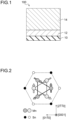
- the magnetic memory element 100 includes a substrate 10, a spin Hall layer 12 on the substrate 10, and an antiferromagnetic layer 14 on the spin Hall layer 12.
- the substrate 10 is made of an insulator such as MgO.
- the spin Hall layer 12 is made of a material that exhibits a spin Hall effect (spin Hall material). Examples of such a material include a non-magnetic heavy metal such as tantalum (Ta), tungsten (W), and platinum (Pt), or a chalcogenide material such as a topological insulator.
- the antiferromagnetic layer 14 is a thin film made of an antiferromagnetic metal containing manganese (Mn).
- Examples of such a gamma-Mn alloy include Mn 1-x Fe x , Mn 1-x Rh x , and Mn 1-x Pd x .
- a mixture of different Mn 3 Xs e.g., a mixture of Mn 3 Sn and Mn 3 Ga
- a mixture of Mn 3 X and an infinitesimal amount of other element e.g., a mixture of Mn 3 Sn and an infinitesimal amount of Cr
- a spin Hall layer is stacked on an antiferromagnetic layer (substrate/ antiferromagnetic layer/ spin Hall layer) may be employed.
- an antiferromagnetic layer may be sandwiched by two spin Hall layers made of spin Hall materials whose spin Hall angles are opposite in sign. The focus below will be on the magnetic memory element 100 shown in FIG. 1 .
- the MgO(5 nm) layer is provided to prevent oxidation of the Mn 3 Sn layer.
- the thickness (nm) of each layer of the magnetic memory element 100 is illustrative only and not restrictive.
- the MgO substrate is annealed at 800 °C for 10 minutes in an ultrahigh vacuum chamber.
- the W(7 nm)/Mn 3 Sn(30 nm)/MgO(5 nm) multilayer film is fabricated on the MgO(110) substrate by a molecular beam epitaxy (MBE) method under ultrahigh vacuum with base pressure of 2 ⁇ 10 -8 Pa.
- the W(7 nm) layer is deposited at a rate of 0.1 ⁇ /s at 300 °C, and subsequently, it is annealed at 800 °C for 10 minutes.
- the Mn 3 Sn(30 nm) layer is fabricated at a rate of 0.25 ⁇ /s with co-evaporation of Mn and Sn.
- the Mn 3 Sn(5 nm) layer is firstly deposited at room temperature and then annealed at 400 °C. Subsequently, the additional Mn 3 Sn(25 nm) layer is deposited at approximately 260 °C.
- RHEED In-situ reflection high energy electron diffraction
- the MgO layer is fabricated at a rate of 0.1 ⁇ /s at room temperature.
- the MgO(110)-substrate/W(7 nm)/Mn 3 Sn(30 nm)/MgO(5 nm) multilayer film is annealed at 650 °C for 30 minutes.
- a sputtering method can be used in the same annealing process to fabricate a multilayer film having the same property as the MBE-fabricated multilayer film.
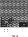
- Mn 3 Sn is an antiferromagnet having a crystal structure called kagome lattice that is a triangle-based lattice in which kagome lattice layers are stacked in [0001] direction as shown in FIG. 2 .
- Mn atoms located at vertices of kagome lattice have a non-collinear magnetic structure in which magnetic moments (directions of localized spins) are oblique to each other by 120 degrees at temperature of 420 K or below due to geometrical frustration.
- a unit of six spins consisting of two sets of three spins residing on a kagome lattice bilayer forms a spin order called a cluster magnetic octupole depicted as hexagon.
- Such a non-collinear magnetic structure can be viewed as ferroic order of the cluster magnetic octupole. This ferroic order breaks the time-reversal symmetry macroscopically.
- the cluster magnetic octupole corresponds to a direction of a fictitious magnetic field in a momentum space (100 to 1000 Tesla (T) in a real space) and Weyl points which have a topological electronic structure. Hence, it is possible to manipulate the responses originating from the fictitious magnetic field and Weyl points based on the direction of the cluster magnetic octupole.
- the magnetic structure shown in FIG. 2 has orthorhombic symmetry, and one of the three magnetic moments of Mn atoms which are triangularly arranged is parallel to an easy axis of magnetization.
- the other two magnetic moments are canted with respect to the easy axis of magnetization, and thus are believed to induce a weak ferromagnetic moment.
- Such an antiferromagnet having a canted magnetic moment to exhibit a tiny magnetization is called a canted antiferromagnet.
- the crystal orientation of Mn 3 Sn plays an important role in enhancement of a readout signal from the magnetic memory element. For example, in an anomalous Hall effect measurement which will be described later, only crystal grains having an out-of-plane component of the magnetic order of the cluster magnetic octupole (i.e., a component perpendicular to a surface of the substrate 10) contribute to a Hall voltage.
- a tensile strain ⁇ is created in the Mn 3 Sn layer in [2-1-10]-direction (in-plane direction) as shown in FIG. 3 .
- This causes the magnetic order of the cluster magnetic octupole to be oriented in an out-of-plane direction, and defines binary states (up, down) on the kagome layers (See FIG. 6B ).
- FIG. 4A shows X-ray diffraction patterns of 28/ ⁇ -scan for the MgO(110)-substrate/W(7 nm) /Mn 3 Sn (30 nm) /MgO (5 nm) samples and the MgO (110) -substrate.
- the X-ray diffraction patterns for the MgO(110)-substrate/W(7 nm)/Mn 3 Sn(30 nm)/MgO(5 nm) samples are obtained when temperatures T A of annealing after forming all the layers of the multilayer film are 650 °C and 700 °C.
- FIG. 4A theoretical spectra for D0 19 -Mn 3 Sn and ⁇ -W are presented.
- FIG. 4B shows X-ray diffraction patterns of ⁇ -scan for ⁇ 02-21 ⁇ planes of the Mn 3 Sn layer, ⁇ 110 ⁇ planes of the W layer, and ⁇ 200 ⁇ planes of the MgO substrate.
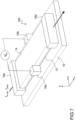
- FIG. 7 shows a configuration of the magnetic memory element 100 with a Hall bar structure.
- a pair of electrodes 16a and 16b made of Au/Ti is disposed on both ends of a sample of the magnetic memory element 100 in a longitudinal direction (x-direction), and a pair of electrodes 18a and 18b made of Au/Ti is disposed in a short direction (y-direction).
- a write current I write or a read current I read flows between the electrodes 16a and 16b, and a Hall voltage V H is detected between the electrodes 18a and 18b.
- the write current I write (pulse current) flows through the spin Hall layer 12 in the longitudinal direction (x-direction).
- This write current generates a spin current in an out-of-plane direction (z-direction) by the spin Hall effect, and this spin current induces an SOT to act on the magnetization of the antiferromagnetic layer 14, thereby allowing reversal of the magnetization.
- a weak bias field H x applying in x-direction affects the magnetization of the antiferromagnetic layer 14, and determines a rotational direction of the magnetization.
- the data (0" or "1") can be written into the antiferromagnetic layer 14.
- the direction of the magnetization of the antiferromagnetic layer 14 can be manipulated depending on the direction of the write current I write .
- the write current I write flowing in +x-direction reverses the magnetization from +z-direction ("1") to -z-direction ("0")
- the write current I write flowing in -x-direction reverses the magnetization from -z-direction ("0") to +z-direction ("1").
- the read current I read (direct current) flows through the antiferromagnetic layer 14 in x-direction.
- This read current generates the Hall voltage V H in y-direction by the anomalous Hall effect.
- the sign of the Hall voltage V H is determined depending on the z-component of the magnetization of the antiferromagnetic layer 14. For example, +z-direction and -z-direction of the magnetization of the antiferromagnetic layer 14 are equivalent to "1" and "0,” respectively.
- the epitaxial strain of about 0.2% can be applied in the Mn 3 Sn layer using the MgO substrate. It is known that the epitaxial strain is typically allowed to increase up to several percent. Thus, the epitaxial strain enables the reversal speed of magnetization in the antiferromagnetic layer 14 to increase up to 1ps to 10ps (10GHz to 1THz).
- the in-plane epitaxial strain in the antiferromagnetic layer allows the magnetic order of the cluster magnetic octupole, which characterizes the antiferromagnetic state, to be oriented in a direction perpendicular to the strain direction, making it possible to define the binary states. Consequently, the antiferromagnet-based magnetic memory element can achieve high-speed write and read operations.
- a magnetic memory element of the second embodiment has the same structure as that of the magnetic memory element 100 of the first embodiment ( FIG. 1 ), and materials of a multilayer film of the magnetic memory element are the same as those in the first embodiment. Also in the second embodiment, Mn 3 Sn will be mentioned as an example of an antiferromagnetic metal.
- the magnetic anisotropy can be manipulated by the piezomagnetic effect in the antiferromagnetic layer.
- M S spontaneous magnetization
- the nearest-neighbor exchange interactions become anisotropic. For example, as shown in the left of FIG.
- Both the samples M1 and M2 are Mn 3 Sn single crystals.
- the sample M1 is under uniaxial stress ⁇ xx along the x-direction applied from right and left sides
- the sample M2 is under uniaxial stress ⁇ yy along the y-direction applied from above and underneath.
- the sample M1 is under a magnetic field H x in [2-1-10] direction (+x-direction)
- the sample M2 is under a magnetic field H y in [01-10] direction (+y-direction).
- Non-Patent Literature Kittaka, S., Taniguchi, H., Yonezawa, S., Yaguchi, H. & Maeno, Y. "Higher-Tc superconducting phase in Sr2RuO4 induced by uniaxial pressure" Phys. Rev. B 81, 180510 (2010 ).
- FIG. 13 shows uniaxial stress dependence of the spontaneous magnetization M S and magnetic susceptibility ⁇ for the samples M1 and M2 at 300 K.
- filled circles denote data points taken under the stress and the magnetic field H x applied along x-direction
- open circles denote data points taken under the stress and the magnetic field H y applied along y-direction.
- the magnetization M increases linearly with the magnetic field except for a low magnetic field region, and its slope represents the magnetic susceptibility ⁇ .
- the stress dependence of M S is found to be linear for both the samples M1 and M2 and nearly isotropic in xy-plane for the sample M2.
- the linear fit to the data indicates that a critical stress ⁇ c at which M S becomes zero is inferred to be about 120 MPa in the tensile stress region ( ⁇ > 0).
- the magnetic susceptibility ⁇ is found to be stress independent. The samples fracture at a stress higher than 300 MPa.
- the magnetic order of the cluster magnetic octupole is oriented in a direction of applying the compressive strain, a readout signal by the anomalous Hall effect or a magnetoresistance effect (to be described later) can be enhanced in the direction of applying the compressive strain.
- a readout signal by the anomalous Hall effect or a magnetoresistance effect (to be described later) can be enhanced in the direction of applying the compressive strain.
- the compressive strain it is possible to manipulate magnitude of magnetization, the anomalous Hall effect, and the magnetoresistance effect. Consequently, the antiferromagnet-based magnetic memory element can achieve high-speed write and read operations.
- the antiferromagnetic layers shown in the first and second embodiments may be single-crystalline films or polycrystalline films. The same holds true for a free layer (antiferromagnetic layer) in the third embodiment below.
- the third embodiment of the invention will be described with reference to FIGS. 16 to 19 .
- the third embodiment is directed to a magnetic memory element including a magnetoresistance element.
- a magnetoresistance element 30 includes a free layer 32 whose magnetization is reversible, a non-magnetic layer 34 which is in contact with the free layer 32, and a reference layer 36 which is in contact with the non-magnetic layer 34 and whose magnetization is fixed in an in-plane direction or an out-of-plane direction.
- the non-magnetic layer 34 is made of an insulator (e.g., MgO, AlOx, MgAl 2 O 4 ).
- Both the free layer 32 and the reference layer 36 are thin films made of the same antiferromagnetic metal as the antiferromagnetic layer 14 shown in FIG. 1 , but the reference layer 36 has a higher coercivity than the free layer 32.
- the free layer 32 preferably has uniaxial strain (epitaxial strain or compressive strain) described in the first and second embodiments.
- the magnetoresistance element 30 serves as a magnetic tunnel junction (MTJ) element.
- MTJ magnetic tunnel junction
- Data "0" and “1" are allocated to the magnetoresistance element 30 according to resistance states.
- the free layer 32 and the reference layer 36 are made of Mn 3 Sn.
- the magnetoresistance element 30 is in a low-resistance state.
- the magnetoresistance element 30 is in a high-resistance state.
- the magnetoresistance element 30 may become a high-resistance state in a parallel state, and become a low-resistance state in an anti-parallel state.
- tunneling magnetoresistance (TMR) effect is observed to be proportional to spin polarization of ferromagnets.
- TMR tunneling magnetoresistance
- antiferromagnet/nonmagnet/antiferromagnet trilayers spin polarization of antiferromagnets is usually negligible, and hence TMR is not observed.
- a spin polarization rate of the antiferromagnet Mn 3 Sn is three orders smaller than that of iron (Fe) which is a ferromagnet.
- TMR ratio (%) is defined as ⁇ (R H - R L )/R H ⁇ ⁇ 100(%).
- the TMR ratio of about 1% is observed in Mn 3 Sn/MgO/Mn 3 Sn multilayer films and is larger than that observed in Fe/MgO/Mn 3 Sn multilayer films.
- the magnetic memory element according to the third embodiment can be served as a magnetic random-access memory (MRAM) element.
- MRAM magnetic random-access memory
- FIG. 18 shows a configuration of a magnetic memory element 200 for an SOT-MRAM.
- the magnetic memory element 200 includes a magnetoresistance element 210, a spin Hall layer 220, a first terminal 231, a second terminal 232, a third terminal 233, and transistors Tr1 and Tr2.
- the spin Hall layer 220 is made of a non-magnetic heavy metal that exhibits a spin Hall effect (such as W and Ta) or made of a chalcogenide material, as with the spin Hall layer 12 shown in FIG. 1 .
- the magnetoresistance element 210 includes a free layer 212 which is stacked on the spin Hall layer 220 and whose magnetization is reversible, a non-magnetic layer 214 stacked on the free layer 212, and a reference layer 216 which is stacked on the non-magnetic layer 214 and whose magnetization is fixed in an out-of-plane direction.
- the materials of the free layer 212, the non-magnetic layer 214, and the reference layer 216 are the same as those of the free layer 32, the non-magnetic layer 34, and the reference layer 36 shown in FIG. 16 , respectively.
- the first terminal 231, the second terminal 232, and the third terminal 233 are made of a metal.
- the first terminal 231 is connected to the reference layer 216, the second terminal 232 is connected to one end portion of the spin Hall layer 220, and the third terminal 233 is connected to the other end portion of the spin Hall layer 220.
- the first terminal 231 is connected to a ground line 240.
- the ground line 240 is set to a ground voltage.
- the ground line 240 may be set to a reference voltage other than the ground voltage.
- Each of the transistors Tr1 and Tr2 is, for example, an N-channel metal oxide semiconductor (NMOS) transistor.
- the second terminal 232 is connected to a drain of the transistor Tr1, and the third terminal 233 is connected to a drain of the transistor Tr2.
- Gates of the transistors Tr1 and Tr2 are connected to a word line WL.
- Sources of the transistors Tr1 and Tr2 are connected to a first bit line BL1 and a second bit line BL2, respectively.
- the magnetization of the free layer 212 and the magnetization of the reference layer 216 are oriented in an out-of-plane direction.
- a weak bias field is applied in a direction of a write current I write , the word line WL is set to high level to turn on the transistors Tr1 and Tr2, one of the first bit line BL1 and the second bit line BL2 is set to high level, and the other bit line is set to low level.
- the write current I write flows through the spin Hall layer 220 in an in-plane direction between the first bit line BL1 and the second bit line BL2 to generate a spin current, which induces an SOT to allow reversal of the magnetization of the free layer 212 and thereby write the data.
- Data to be written can be changed depending on the direction of the write current I write .
- the word line WL is set to high level to turn on the transistors Tr1 and Tr2, one of the bit lines (second bit line BL2) is set to high level, and the other of the bit lines (first bit line BL1) is set to an open state.
- a read current I read flows from the second bit line BL2 in high level into the ground line 240 through the third terminal 233, the spin Hall layer 220, the free layer 212, the non-magnetic layer 214, the reference layer 216, and the first terminal 231.
- FIG. 19 shows a configuration of a magnetic memory element 300 for an STT-MRAM whose magnetization is reversed by a spin transfer torque (STT).
- the magnetic memory element 300 includes a magnetoresistance element 310, a first terminal 321, a second terminal 322, and a transistor Tr.
- the magnetoresistance element 310 includes a reference layer 316 whose magnetization is fixed in an out-of-plane direction, a non-magnetic layer 314 stacked on the reference layer 316, and a free layer 312 which is stacked on the non-magnetic layer 314 and whose magnetization is reversible.
- the materials of the free layer 312, the non-magnetic layer 314, and the reference layer 316 are the same as those of the free layer 32, the non-magnetic layer 34, and the reference layer 36 shown in FIG. 16 , respectively.
- the word line WL is set to high level to turn on the transistor Tr, and a write current I write flows in an out-of-plane direction between the bit line BL and the source line SL. This induces an STT to allow reversal of the magnetization of the free layer 312 and thereby write the data. Data to be written can be changed depending on the direction of the write current I write .
- the word line WL is set to high level to turn on the transistor Tr, and a read current I read flows between the bit line BL and the source line SL.
- a read current I read flows between the bit line BL and the source line SL.
- an ultrathin ferromagnetic layer made of a ferromagnet (e.g., CoFeB) with a thickness of 2nm or less may be stacked on the antiferromagnetic layer as the free layer 212 to employ another magnetoresistance element of [antiferromagnetic layer/ferromagnetic layer] (free layer)/non-magnetic layer/ferromagnetic layer (reference layer).
- This stacking structure may be turned upside down to employ still another magnetoresistance element of ferromagnetic layer (reference layer)/non-magnetic layer/[ferromagnetic layer/antiferromagnetic layer] (free layer) in FIG. 19 .
Landscapes
- Engineering & Computer Science (AREA)
- Computer Hardware Design (AREA)
- Hall/Mr Elements (AREA)
- Mram Or Spin Memory Techniques (AREA)
Applications Claiming Priority (2)
| Application Number | Priority Date | Filing Date | Title |
|---|---|---|---|
| JP2022088105 | 2022-05-30 | ||
| PCT/JP2023/019977 WO2023234269A1 (ja) | 2022-05-30 | 2023-05-29 | 磁気メモリ素子、情報処理システム、及び磁気メモリ素子の制御方法 |
Publications (1)
| Publication Number | Publication Date |
|---|---|
| EP4535954A1 true EP4535954A1 (en) | 2025-04-09 |
Family
ID=89025102
Family Applications (1)
| Application Number | Title | Priority Date | Filing Date |
|---|---|---|---|
| EP23816026.1A Pending EP4535954A1 (en) | 2022-05-30 | 2023-05-29 | Magnetic memory element, information processing system, and mehod for controlling magnetic memory element |
Country Status (4)
| Country | Link |
|---|---|
| US (1) | US20250351732A1 (https=) |
| EP (1) | EP4535954A1 (https=) |
| JP (1) | JP7784762B2 (https=) |
| WO (1) | WO2023234269A1 (https=) |
Families Citing this family (1)
| Publication number | Priority date | Publication date | Assignee | Title |
|---|---|---|---|---|
| WO2025127136A1 (ja) * | 2023-12-14 | 2025-06-19 | Jsr株式会社 | Antiferromagnetic material with large anomalous hall effect |
Family Cites Families (4)
| Publication number | Priority date | Publication date | Assignee | Title |
|---|---|---|---|---|
| WO2017018391A1 (ja) | 2015-07-24 | 2017-02-02 | 国立大学法人東京大学 | メモリ素子 |
| US9837602B2 (en) | 2015-12-16 | 2017-12-05 | Western Digital Technologies, Inc. | Spin-orbit torque bit design for improved switching efficiency |
| US11621391B2 (en) | 2018-12-28 | 2023-04-04 | Intel Corporation | Antiferromagnet based spin orbit torque memory device |
| WO2020166722A1 (ja) | 2019-02-15 | 2020-08-20 | 国立大学法人東京大学 | スピントロニクス素子及び磁気メモリ装置 |
-
2023
- 2023-05-29 WO PCT/JP2023/019977 patent/WO2023234269A1/ja not_active Ceased
- 2023-05-29 JP JP2024524858A patent/JP7784762B2/ja active Active
- 2023-05-29 US US18/869,003 patent/US20250351732A1/en active Pending
- 2023-05-29 EP EP23816026.1A patent/EP4535954A1/en active Pending
Also Published As
| Publication number | Publication date |
|---|---|
| JP7784762B2 (ja) | 2025-12-12 |
| WO2023234269A1 (ja) | 2023-12-07 |
| JPWO2023234269A1 (https=) | 2023-12-07 |
| US20250351732A1 (en) | 2025-11-13 |
Similar Documents
| Publication | Publication Date | Title |
|---|---|---|
| US10529775B2 (en) | Two-terminal spintronic devices | |
| US9105832B2 (en) | Spin hall effect magnetic apparatus, method and applications | |
| JP4873338B2 (ja) | スピン注入デバイス及びこれを用いた磁気装置 | |
| US10490247B2 (en) | Memory element | |
| EP2863434B1 (en) | High speed low power magnetic devices based on current induced spin-momentum transfer | |
| US10008248B2 (en) | Circuits and devices based on enhanced spin hall effect for efficient spin transfer torque | |
| EP2220651B1 (en) | High speed low power magnetic devices based on current induced spin-momentum transfer | |
| JP4954445B2 (ja) | 非晶質フェリ磁性合金を使用してスピン偏極電流で書き込みを行なう磁気メモリ及びその書き込み方法 | |
| KR20220029381A (ko) | 쌍극자 결합 스핀 궤도 토크 구조 | |
| US20150357015A1 (en) | Current Induced Spin-Momentum Transfer Stack With Dual Insulating Layers | |
| US10686127B2 (en) | Antiferromagnet and heavy metal multilayer magnetic systems for switching magnetization using spin-orbit torque | |
| WO2022220251A1 (ja) | 磁気メモリ素子 | |
| EP3185245A1 (en) | Antiferromagnetic memory device | |
| JP2018037616A (ja) | 磁気トンネル接合素子 | |
| EP4535954A1 (en) | Magnetic memory element, information processing system, and mehod for controlling magnetic memory element | |
| Kaidatzis et al. | “Metal oxides in magnetic memories”: Current status and future perspectives | |
| US20260096351A1 (en) | Magnetic memory element, magnetic memory device, photonic spin register, data writing method, data reading method, apparatus, and information processing system | |
| JP5424178B2 (ja) | スピン注入デバイス及びこれを用いた磁気装置 | |
| US12230308B2 (en) | Non-local antiferromagnetic memory storage | |
| Gould et al. | Novel spintronic devices using local anisotropy engineering in (Ga, Mn) As |
Legal Events
| Date | Code | Title | Description |
|---|---|---|---|
| STAA | Information on the status of an ep patent application or granted ep patent |
Free format text: STATUS: THE INTERNATIONAL PUBLICATION HAS BEEN MADE |
|
| PUAI | Public reference made under article 153(3) epc to a published international application that has entered the european phase |
Free format text: ORIGINAL CODE: 0009012 |
|
| STAA | Information on the status of an ep patent application or granted ep patent |
Free format text: STATUS: REQUEST FOR EXAMINATION WAS MADE |
|
| 17P | Request for examination filed |
Effective date: 20250102 |
|
| AK | Designated contracting states |
Kind code of ref document: A1 Designated state(s): AL AT BE BG CH CY CZ DE DK EE ES FI FR GB GR HR HU IE IS IT LI LT LU LV MC ME MK MT NL NO PL PT RO RS SE SI SK SM TR |
|
| DAV | Request for validation of the european patent (deleted) | ||
| DAX | Request for extension of the european patent (deleted) | ||
| REG | Reference to a national code |
Ref country code: DE Ref legal event code: R079 Free format text: PREVIOUS MAIN CLASS: H10B0061000000 Ipc: G11C0011160000 |