EP4517833A1 - Siliciumcarbid-mosfet-wechselrichterschaltung und verfahren zur steuerung einer siliciumcarbid-mosfet-wechselrichterschaltung - Google Patents
Siliciumcarbid-mosfet-wechselrichterschaltung und verfahren zur steuerung einer siliciumcarbid-mosfet-wechselrichterschaltung Download PDFInfo
- Publication number
- EP4517833A1 EP4517833A1 EP23903116.4A EP23903116A EP4517833A1 EP 4517833 A1 EP4517833 A1 EP 4517833A1 EP 23903116 A EP23903116 A EP 23903116A EP 4517833 A1 EP4517833 A1 EP 4517833A1
- Authority
- EP
- European Patent Office
- Prior art keywords
- silicon carbide
- mosfet
- high concentration
- region
- inverter circuit
- Prior art date
- Legal status (The legal status is an assumption and is not a legal conclusion. Google has not performed a legal analysis and makes no representation as to the accuracy of the status listed.)
- Pending
Links
Images






Classifications
-
- H—ELECTRICITY
- H02—GENERATION; CONVERSION OR DISTRIBUTION OF ELECTRIC POWER
- H02M—APPARATUS FOR CONVERSION BETWEEN AC AND AC, BETWEEN AC AND DC, OR BETWEEN DC AND DC, AND FOR USE WITH MAINS OR SIMILAR POWER SUPPLY SYSTEMS; CONVERSION OF DC OR AC INPUT POWER INTO SURGE OUTPUT POWER; CONTROL OR REGULATION THEREOF
- H02M7/00—Conversion of AC power input into DC power output; Conversion of DC power input into AC power output
- H02M7/42—Conversion of DC power input into AC power output without possibility of reversal
- H02M7/44—Conversion of DC power input into AC power output without possibility of reversal by static converters
- H02M7/48—Conversion of DC power input into AC power output without possibility of reversal by static converters using discharge tubes with control electrode or semiconductor devices with control electrode
- H02M7/53—Conversion of DC power input into AC power output without possibility of reversal by static converters using discharge tubes with control electrode or semiconductor devices with control electrode using devices of a triode or transistor type requiring continuous application of a control signal
- H02M7/537—Conversion of DC power input into AC power output without possibility of reversal by static converters using discharge tubes with control electrode or semiconductor devices with control electrode using devices of a triode or transistor type requiring continuous application of a control signal using semiconductor devices only, e.g. single switched pulse inverters
- H02M7/5387—Conversion of DC power input into AC power output without possibility of reversal by static converters using discharge tubes with control electrode or semiconductor devices with control electrode using devices of a triode or transistor type requiring continuous application of a control signal using semiconductor devices only, e.g. single switched pulse inverters in a bridge configuration
-
- H—ELECTRICITY
- H03—ELECTRONIC CIRCUITRY
- H03K—PULSE TECHNIQUE
- H03K17/00—Electronic switching or gating, i.e. not by contact-making and –breaking
- H03K17/08—Modifications for protecting switching circuit against overcurrent or overvoltage
- H03K17/081—Modifications for protecting switching circuit against overcurrent or overvoltage without feedback from the output circuit to the control circuit
- H03K17/0812—Modifications for protecting switching circuit against overcurrent or overvoltage without feedback from the output circuit to the control circuit by measures taken in the control circuit
- H03K17/08122—Modifications for protecting switching circuit against overcurrent or overvoltage without feedback from the output circuit to the control circuit by measures taken in the control circuit in field-effect transistor switches
-
- H—ELECTRICITY
- H03—ELECTRONIC CIRCUITRY
- H03K—PULSE TECHNIQUE
- H03K17/00—Electronic switching or gating, i.e. not by contact-making and –breaking
- H03K17/28—Modifications for introducing a time delay before switching
- H03K17/284—Modifications for introducing a time delay before switching in field effect transistor switches
-
- H—ELECTRICITY
- H10—SEMICONDUCTOR DEVICES; ELECTRIC SOLID-STATE DEVICES NOT OTHERWISE PROVIDED FOR
- H10D—INORGANIC ELECTRIC SEMICONDUCTOR DEVICES
- H10D62/00—Semiconductor bodies, or regions thereof, of devices having potential barriers
- H10D62/10—Shapes, relative sizes or dispositions of the regions of the semiconductor bodies; Shapes of the semiconductor bodies
- H10D62/102—Constructional design considerations for preventing surface leakage or controlling electric field concentration
- H10D62/103—Constructional design considerations for preventing surface leakage or controlling electric field concentration for increasing or controlling the breakdown voltage of reverse-biased devices
- H10D62/105—Constructional design considerations for preventing surface leakage or controlling electric field concentration for increasing or controlling the breakdown voltage of reverse-biased devices by having particular doping profiles, shapes or arrangements of PN junctions; by having supplementary regions, e.g. junction termination extension [JTE]
- H10D62/106—Constructional design considerations for preventing surface leakage or controlling electric field concentration for increasing or controlling the breakdown voltage of reverse-biased devices by having particular doping profiles, shapes or arrangements of PN junctions; by having supplementary regions, e.g. junction termination extension [JTE] having supplementary regions doped oppositely to or in rectifying contact with regions of the semiconductor bodies, e.g. guard rings with PN or Schottky junctions
- H10D62/107—Buried supplementary regions, e.g. buried guard rings
-
- H—ELECTRICITY
- H10—SEMICONDUCTOR DEVICES; ELECTRIC SOLID-STATE DEVICES NOT OTHERWISE PROVIDED FOR
- H10D—INORGANIC ELECTRIC SEMICONDUCTOR DEVICES
- H10D62/00—Semiconductor bodies, or regions thereof, of devices having potential barriers
- H10D62/10—Shapes, relative sizes or dispositions of the regions of the semiconductor bodies; Shapes of the semiconductor bodies
- H10D62/124—Shapes, relative sizes or dispositions of the regions of semiconductor bodies or of junctions between the regions
- H10D62/126—Top-view geometrical layouts of the regions or the junctions
- H10D62/127—Top-view geometrical layouts of the regions or the junctions of cellular field-effect devices, e.g. multicellular DMOS transistors or IGBTs
-
- H—ELECTRICITY
- H10—SEMICONDUCTOR DEVICES; ELECTRIC SOLID-STATE DEVICES NOT OTHERWISE PROVIDED FOR
- H10D—INORGANIC ELECTRIC SEMICONDUCTOR DEVICES
- H10D62/00—Semiconductor bodies, or regions thereof, of devices having potential barriers
- H10D62/10—Shapes, relative sizes or dispositions of the regions of the semiconductor bodies; Shapes of the semiconductor bodies
- H10D62/13—Semiconductor regions connected to electrodes carrying current to be rectified, amplified or switched, e.g. source or drain regions
- H10D62/149—Source or drain regions of field-effect devices
- H10D62/151—Source or drain regions of field-effect devices of IGFETs
- H10D62/156—Drain regions of DMOS transistors
- H10D62/157—Impurity concentrations or distributions
-
- H—ELECTRICITY
- H10—SEMICONDUCTOR DEVICES; ELECTRIC SOLID-STATE DEVICES NOT OTHERWISE PROVIDED FOR
- H10D—INORGANIC ELECTRIC SEMICONDUCTOR DEVICES
- H10D62/00—Semiconductor bodies, or regions thereof, of devices having potential barriers
- H10D62/10—Shapes, relative sizes or dispositions of the regions of the semiconductor bodies; Shapes of the semiconductor bodies
- H10D62/17—Semiconductor regions connected to electrodes not carrying current to be rectified, amplified or switched, e.g. channel regions
- H10D62/393—Body regions of DMOS transistors or IGBTs
-
- H—ELECTRICITY
- H10—SEMICONDUCTOR DEVICES; ELECTRIC SOLID-STATE DEVICES NOT OTHERWISE PROVIDED FOR
- H10D—INORGANIC ELECTRIC SEMICONDUCTOR DEVICES
- H10D84/00—Integrated devices formed in or on semiconductor substrates that comprise only semiconducting layers, e.g. on Si wafers or on GaAs-on-Si wafers
- H10D84/101—Integrated devices comprising main components and built-in components, e.g. IGBT having built-in freewheel diode
- H10D84/141—VDMOS having built-in components
- H10D84/143—VDMOS having built-in components the built-in components being PN junction diodes
- H10D84/144—VDMOS having built-in components the built-in components being PN junction diodes in antiparallel diode configurations
-
- H—ELECTRICITY
- H10—SEMICONDUCTOR DEVICES; ELECTRIC SOLID-STATE DEVICES NOT OTHERWISE PROVIDED FOR
- H10D—INORGANIC ELECTRIC SEMICONDUCTOR DEVICES
- H10D84/00—Integrated devices formed in or on semiconductor substrates that comprise only semiconducting layers, e.g. on Si wafers or on GaAs-on-Si wafers
- H10D84/80—Integrated devices formed in or on semiconductor substrates that comprise only semiconducting layers, e.g. on Si wafers or on GaAs-on-Si wafers characterised by the integration of at least one component covered by groups H10D12/00 or H10D30/00, e.g. integration of IGFETs
- H10D84/811—Combinations of field-effect devices and one or more diodes, capacitors or resistors
-
- H—ELECTRICITY
- H10—SEMICONDUCTOR DEVICES; ELECTRIC SOLID-STATE DEVICES NOT OTHERWISE PROVIDED FOR
- H10D—INORGANIC ELECTRIC SEMICONDUCTOR DEVICES
- H10D30/00—Field-effect transistors [FET]
- H10D30/60—Insulated-gate field-effect transistors [IGFET]
- H10D30/64—Double-diffused metal-oxide semiconductor [DMOS] FETs
- H10D30/66—Vertical DMOS [VDMOS] FETs
- H10D30/668—Vertical DMOS [VDMOS] FETs having trench gate electrodes, e.g. UMOS transistors
-
- H—ELECTRICITY
- H10—SEMICONDUCTOR DEVICES; ELECTRIC SOLID-STATE DEVICES NOT OTHERWISE PROVIDED FOR
- H10D—INORGANIC ELECTRIC SEMICONDUCTOR DEVICES
- H10D62/00—Semiconductor bodies, or regions thereof, of devices having potential barriers
- H10D62/80—Semiconductor bodies, or regions thereof, of devices having potential barriers characterised by the materials
- H10D62/83—Semiconductor bodies, or regions thereof, of devices having potential barriers characterised by the materials being Group IV materials, e.g. B-doped Si or undoped Ge
- H10D62/832—Semiconductor bodies, or regions thereof, of devices having potential barriers characterised by the materials being Group IV materials, e.g. B-doped Si or undoped Ge being Group IV materials comprising two or more elements, e.g. SiGe
- H10D62/8325—Silicon carbide
Definitions
- the present invention relates to a silicon carbide MOSFET inverter circuit, and a control method for the silicon carbide MOSFET inverter circuit.
- Patent document 1 describes "a silicon carbide MOSFET inverter circuit capable of suppressing the expansion of stacking faults during deadtime".
- a silicon carbide MOSFET inverter circuit in which a first silicon carbide MOSFET and a second silicon carbide MOSFET are connected in series is provided, wherein: a current density of a transient current flowing in a built-in diode of a to-be-controlled MOSFET is less than 1000A/cm 2 during a turn-off period of the to-be-controlled MOSFET; a gate of the to-be-controlled MOSFET is turned on during the turn-off period such that a saturation current period in which the transient current becomes a saturation current is less than 5 ⁇ s; and the to-be-controlled MOSFET is the first silicon carbide MOSFET or the second silicon carbide MOSFET.
- the to-be-controlled MOSFET includes: a drift region of a first conductivity type provided in a silicon carbide semiconductor substrate; a base region of a second conductivity type provided above the drift region in the semiconductor substrate; and a high concentration region of the second conductivity type having a higher doping concentration than the base region in the semiconductor substrate, wherein an area proportion of the high concentration region relative to an area of the drift region in a top view may be less than 50%.
- the area proportion may be 44% or more and 48% or less.
- the doping concentration of the high concentration region may be 4E18cm -3 or more and 1E19cm -3 or less.
- the to-be-controlled MOSFET includes: a drift region of a first conductivity type provided in a silicon carbide semiconductor substrate; a base region of a second conductivity type provided above the drift region in the semiconductor substrate; a high concentration region of the second conductivity type having a higher doping concentration than the base region in the semiconductor substrate; a plurality of trench portions extending in a predetermined extending direction at a front surface side of the semiconductor substrate; and a plurality of contact regions of the second conductivity type having a higher doping concentration than the base region, respectively extending in the extending direction of the plurality of trench portions, between adjacent trench portions among the plurality of trench portions, wherein the high concentration region may include a plurality of first high concentration portions, respectively extending in the extending direction of the plurality of trench portions, below each of the plurality of trench portions.
- the high concentration region may include a plurality of second high concentration portions, respectively extending in the extending direction of the plurality of trench portions, below each of the plurality of contact regions.
- the high concentration region may include a plurality of third high concentration portions extending in a stripe shape traversing the plurality of first high concentration portions and the plurality of second high concentration portions in an arrangement direction of the plurality of trench portions.
- a separation distance between third high concentration portions that are adjacent in the extending direction of the plurality of trench portions among the plurality of third high concentration portion provided in the stripe shape may be 24 ⁇ m or more and 40 ⁇ m or less.
- an area proportion of the high concentration region relative to an area of the drift region in a top view may be less than 50%.
- the doping concentration of the high concentration region may be 4E18cm -3 or more and 1E19cm -3 or less.
- the to-be-controlled MOSFET includes: a drift region of a first conductivity type provided in a silicon carbide semiconductor substrate; a base region of a second conductivity type provided above the drift region in the semiconductor substrate; a high concentration region of the second conductivity type having a higher doping concentration than the base region in the semiconductor substrate; a plurality of trench portions extending in a predetermined extending direction at a front surface side of the semiconductor substrate; and a plurality of contact regions of the second conductivity type having a higher doping concentration than the base region, arranged in an island shape spaced apart from each of adjacent trench portions, between the adjacent trench portions among the plurality of trench portions, wherein the high concentration region may include a plurality of first high concentration portions, respectively extending in the extending direction, below each of the plurality of trench portions.
- each of the plurality of contact regions may be provided in contact with each of first high concentration portions provided below each of the adjacent trench portions among the plurality of first high concentration portions.
- a separation distance between contact regions that are adjacent in the extending direction of the plurality of trench portions among the plurality of contact regions may be 2 ⁇ m or more and 4 ⁇ m or less.
- an area proportion of the high concentration region relative to an area of the drift region in a top view may be less than 50%.
- the area proportion may be 44% or more and 48% or less.
- Any silicon carbide MOSFET inverter circuit described above may include a first diode connected to the first silicon carbide MOSFET in an anti-parallel manner, and a second diode connected to the second silicon carbide MOSFET in an anti-parallel manner.
- a bus voltage applied to the to-be-controlled MOSFET may be 2/3 or less of a breakdown voltage of the to-be-controlled MOSFET.
- one side in a direction parallel to a depth direction of a semiconductor substrate is referred to as an "upper” side, and the other side is referred to as a “lower” side.
- One surface of two principal surfaces of a substrate, a layer or other member is referred to as an upper surface, and another surface is referred to as a lower surface.
- Directions of "upper”, “lower”, “front”, and “back” are not limited to direction of gravity, or a direction of mounting on a substrate or the like in implementation of a silicon carbide MOSFET inverter circuit.
- an XY plane refers to a plane parallel to an upper surface of the semiconductor substrate
- the Z axis refers to a depth direction of the semiconductor substrate.
- Each example embodiment shows an example in which a first conductivity type is set as an N type, and a second conductivity type is set as a P type; however, the first conductivity type may be the P type, and the second conductivity type may be the N type.
- conductivity types of the substrate, the layer, a region, and the like in each example embodiment respectively have opposite polarities.
- electrons or holes are meant to be majority carriers, respectively.
- the sign "+” or “-” given to the character “N” or “P” means having a higher or lower doping concentration than layers or regions without it, respectively.
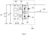
- Fig. 1 shows an example of a silicon carbide MOSFET inverter circuit 100.
- the silicon carbide MOSFET inverter circuit 100 includes a first silicon carbide MOSFET 22, a second silicon carbide MOSFET 26, and a control circuit 30.
- the silicon carbide MOSFET inverter circuit 100 may include a first diode 23 and a second diode 27.
- the silicon carbide MOSFET inverter circuit 100 may be connected to a direct current power source 10, a smoothing capacitor 12, and a load 40.
- an H-bridge may be provided by two sets of silicon carbide MOSFET inverter circuits 100 connected in parallel to the load 40.
- a three-phase inverter may be provided by three sets of silicon carbide MOSFET inverter circuits 100 connected in parallel.
- the silicon carbide MOSFET inverter circuit 100 is an inverter circuit in which the first silicon carbide MOSFET 22 and the second silicon carbide MOSFET 26 are connected in series.
- the silicon carbide MOSFET inverter circuit 100 may be an inverter circuit in which a DC voltage applied from the direct current power source 10 is converted into an AC voltage.
- the DC voltage of the direct current power source 10 may be input to the silicon carbide MOSFET inverter circuit 100 after being smoothed by the smoothing capacitor 12.
- the AC voltage converted to by the silicon carbide MOSFET inverter circuit 100 may be applied to the load 40.
- the first silicon carbide MOSFET 22 includes a first built-in diode 21.
- the first built-in diode 21 may be a parasitic diode formed between a source electrode and a drain electrode due to a configuration of the first silicon carbide MOSFET 22.
- the first diode 23 is connected to the first silicon carbide MOSFET 22 in an anti-parallel manner.
- the first diode 23 may be a Schottky barrier diode.
- the first diode 23 may shunt the current flowing in the first built-in diode 21 at the time of regeneration of the first silicon carbide MOSFET 22, or may cause the current not to flow in the first built-in diode 21.
- expansion of stacking faults generated by the current flowing in the first built-in diode 21 at the time of regeneration of the first silicon carbide MOSFET 22 can be suppressed, and a rise of an on-resistance and a rise of an on-voltage of the first silicon carbide MOSFET 22 can be suppressed.
- the second silicon carbide MOSFET 26 includes a second built-in diode 25.
- the second built-in diode 25 may be a parasitic diode formed between a source electrode and a drain electrode due to the second silicon carbide MOSFET 26.
- the second diode 27 is connected to the second silicon carbide MOSFET 26 in an anti-parallel manner.
- the second diode 27 may be a Schottky barrier diode.
- the second diode 27 may shunt the current flowing in the second built-in diode 25 at the time of regeneration of the second silicon carbide MOSFET 26, or may cause the current not to flow in the second built-in diode 25.
- expansion of stacking faults generated by the current flowing in the second built-in diode 25 at the time of regeneration of the second silicon carbide MOSFET 26 can be suppressed, and a rise of an on-resistance and a rise of an on-voltage of the second silicon carbide MOSFET 26 can be suppressed.
- a MOSFET that is a to-be-controlled object upon operation of the inverter circuit is referred to as a to-be-controlled MOSFET 20. That is, the to-be-controlled MOSFET 20 is the first silicon carbide MOSFET 22 or the second silicon carbide MOSFET 26.
- the control circuit 30 controls on/off of the to-be-controlled MOSFET 20 by applying a gate voltage to the to-be-controlled MOSFET 20.
- a bus voltage is applied from the direct current power source 10 to the to-be-controlled MOSFET 20.
- a bus voltage applied to the to-be-controlled MOSFET 20 upon a normal operation may be 2/3 or less of a breakdown voltage of the to-be-controlled MOSFET 20.
- the control circuit 30 is provided to each of the first silicon carbide MOSFET 22 and the second silicon carbide MOSFET 26, but not limited thereto. That is, a control circuit 30 may be integrally provided as long as it is a circuit that is capable of controlling each of the first silicon carbide MOSFET 22 and the second silicon carbide MOSFET 26.
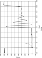
- Fig. 2A shows an example of a temporal change of a drain-source voltage Vds of a first silicon carbide MOSFET 22.
- the horizontal axis indicates time T, and the vertical axis indicates a drain-source voltage Vds of the first silicon carbide MOSFET 22.
- a breakdown voltage of the to-be-controlled MOSFET 20 in the present example is 1200V, and a bus voltage is 800V. That is, the bus voltage applied to the to-be-controlled MOSFET 20 of the present example is 2/3 of the breakdown voltage of the to-be-controlled MOSFET 20.
- a gate voltage is applied to the second silicon carbide MOSFET 26, to turn on the second silicon carbide MOSFET 26.
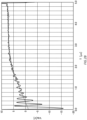
- Fig. 2B shows an enlarged drawing of a region S in Fig. 2A .
- Dashed lines of Fig. 2B indicate approximate curves of the drain-source voltage Vds.
- a conductivity modulation occurs due to holes injected into an energized portion and the drain-source voltage Vds gradually rises.
- Fig. 3 shows an example of a temporal change of a current flowing in a second built-in diode 25 of the second silicon carbide MOSFET 26.
- the horizontal axis indicates time T, and the vertical axis indicates a current flowing in the second built-in diode 25 of the second silicon carbide MOSFET 26.
- a transient current starts to flow in the second built-in diode 25, and the transient current becomes a saturation current Ic.
- a current density of the transient current flowing in the second built-in diode 25 of the second silicon carbide MOSFET 26 may be less than 1000A/cm 2 . That is, the current density of the saturation current Ic may be less than 1000A/cm 2 . As an example, the current density of the saturation current Ic is 900A/cm 2 .
- the second silicon carbide MOSFET 26 and the second built-in diode 25 during the turn-off period of the first silicon carbide MOSFET 22 is described, but the first silicon carbide MOSFET 22 and the first built-in diode 21 during a turn-off period of the second silicon carbide MOSFET 26 operates in a similar cycle except for a phase of on/off being shifted by 90 degrees.
- the current density of the transient current flowing in the built-in diode of the to-be-controlled MOSFET may be less than 1000A/cm 2 .
- a current density of the transient current flowing in the second built-in diode 25 of the second silicon carbide MOSFET 26 may be less than 1000A/cm 2
- the current density of the transient current flowing in the first built-in diode 21 of the first silicon carbide MOSFET 22 may be less than 1000A/cm 2 .
- the control circuit 30 turns on a gate of the to-be-controlled MOSFET 20 during the turn-off period of the to-be-controlled MOSFET 20 such that a saturation current period in which a transient current becomes a saturation current Ic is less than 5 ⁇ s.
- an expansion of stacking faults of the to-be-controlled MOSFET 20 can be suppressed. That is, by performing the synchronization control on the to-be-controlled MOSFET 20 to cause the saturation current period in which the transient current becomes the saturation current Ic to be less than 5 ⁇ s, the current flowing in the built-in diode during a period in which an amount of holes injected in the to-be-controlled MOSFET 20 is small can be reduced, and the frequency of recombining the electrons and the holes can be reduced to suppress the expansion of the stacking faults.
- Fig. 4 shows an example of an on-voltage rising rate ⁇ Von of the to-be-controlled MOSFET 20 with respect to a length of a saturation current period.
- the vertical axis indicates a rising rate with respect to an initial state of the on-voltage of the on-voltage after operating the to-be-controlled MOSFET 20 for predetermined number of times, and the horizontal axis indicates a length of the saturation current period when the to-be-controlled MOSFET 20 is operated for the predetermined number of times.
- the failure of the to-be-controlled MOSFET 20 can be reduced. That is, the on-voltage rising rate ⁇ Von of the to-be-controlled MOSFET 20 is less than 5% that is a reference of determining the failure.
- the silicon carbide MOSFET inverter circuit 100 of the present example can relax these restrictions and can reduce a constraint upon driving the silicon carbide MOSFET inverter circuit 100. Furthermore, by increasing a current density of the current flowing in the built-in diode and/or extending a period during which the current flow in the built-in diode, an amount of current used for regeneration of the to-be-controlled MOSFET 20 can be increased, and an efficiency of regeneration of the to-be-controlled MOSFET 20 can be increased.
- a diode that is connected to the to-be-controlled MOSFET 20 in an anti-parallel manner for example, the first diode 23 and the second diode 27 in Fig. 1 . That is, by providing such a diode, the current flowing in the built-in diode at the time of regeneration of the to-be-controlled MOSFET 20 may be suppressed.
- the silicon carbide MOSFET inverter circuit 100 of the present example may not include the first diode 23 and the second diode 27. If the first diode 23 and the second diode 27 are not provided, the silicon carbide MOSFET inverter circuit 100 can be miniaturized and inexpensive.
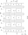
- Fig. 5A shows an example of an upper surface of the to-be-controlled MOSFET 20.
- the to-be-controlled MOSFET 20 includes a contact region 215, a source region 216, and a trench portion 240 on a front surface of a silicon carbide semiconductor substrate 210.
- the to-be-controlled MOSFET 20 includes a high concentration region 230 below the front surface of the silicon carbide semiconductor substrate 210. That is, the high concentration region 230 is indicated with dashed lines because it is not exposed on the front surface of the silicon carbide semiconductor substrate 210.
- the high concentration region 230 includes a first high concentration portion 232, a second high concentration portion 234, and a third high concentration portion 236.
- the to-be-controlled MOSFET 20 includes a plurality of trench portions 240 extending in a predetermined extending direction on the front surface of the semiconductor substrate 210.
- the extending direction of the trench portion 240 of the present example is a Y axis direction.
- the to-be-controlled MOSFET 20 includes a plurality of contact regions 215 of a second conductivity type, respectively extending in the extending direction of the plurality of trench portions 240, between adjacent trench portions among the plurality of trench portions 240.
- a contact region 215a among the plurality of contact regions 215 is extending, between adjacent trench portions 240a and 240b among the plurality of trench portions 240, in the Y axis direction.
- the contact region 215 is of P+ type, as an example.
- the high concentration region 230 is a region of the second conductivity type.
- the high concentration region 230 may be a region that functions as a hole injection path.
- the high concentration region 230 includes a plurality of first high concentration portions 232 respectively extending in the extending direction of the plurality of trench portions 240, below each of the plurality of trench portions 240.
- the first high concentration portion 232 extends in the Y axis direction that is the extending direction of the trench portion 240.
- the high concentration region 230 includes a plurality of second high concentration portions 234 respectively extending in the extending direction of the plurality of trench portions 240, below each of the plurality of contact regions 215.
- the second high concentration portion 234 extends in the Y axis direction that is the extending direction of the trench portion 240.
- the high concentration region 230 includes a plurality of third high concentration portions 236 extending in a stripe shape by traversing the plurality of first high concentration portions 232 and the plurality of second high concentration portions 234 in an arrangement direction of the plurality of trench portions 240.
- the arrangement direction of the plurality of trench portions 240 of the present example is an X axis direction
- the third high concentration portion 236 extends in a stripe shape by traversing the plurality of first high concentration portions 232 and the plurality of second high concentration portions 234 in the X axis direction that is the arrangement direction of the plurality of trench portions 240.
- the third high concentration portion 236 may be provided as a bridge for conducting the plurality of first high concentration portions 232 and the plurality of second high concentration portions 234.
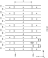
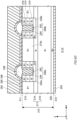
- Fig. 5B shows an example of a cross section including a high concentration region 230 of the to-be-controlled MOSFET 20. That is, an example of a cross section of a plane including the region indicated with the dashed lines in Fig. 5A is indicated.
- the to-be-controlled MOSFET 20 includes a second drift region 219, which is described below, in the plane including the high concentration region 230.
- a width W1 of the first high concentration portion 232 may be 0.7 ⁇ m or more, and 1.1 ⁇ m or less. As an example, the width W1 of the first high concentration portion 232 is 0.9 ⁇ m.
- a width W2 of the second high concentration portion 234 may be 0.55 ⁇ m or more, and 0.95 ⁇ m or less. As an example, the width W2 of the second high concentration portion 234 is 0.75 ⁇ m.
- a separation distance between the third high concentration portions 236 that are adjacent in the extending direction of the plurality of trench portions 240 among the plurality of third high concentration portions 236 provided in the stripe shape may be 24 ⁇ m or more and 40 ⁇ m or less. That is, a separation distance L1 between third high concentration portion 236a and 236b that are adjacent in the Y axis direction that is the extending direction of the trench portion 240 among the plurality of third high concentration portions 236 may be 24 ⁇ m or more and 40 ⁇ m or less. As an example, the separation distance L1 is 32 ⁇ m.
- a width W3 of the third high concentration portion 236 may be 0.8 ⁇ m or more, and 1.2 ⁇ m or less. As an example, the width W3 of the third high concentration portion 236 is 1.0 ⁇ m.
- an area proportion of the high concentration region 230 relative to an area of a drift region 217 may be less than 50%. That is, a ratio of the area of the high concentration region 230 occupying on the area of the region shown in Fig. 5B may be less than 50%.
- the drift region 217 will be described below.
- the area proportion of the high concentration region 230 relative to the area of the drift region 217 can be less than 50%.
- a hole injection amount during a period in which a current is flowing in the built-in diode can be suppressed. That is, by causing the area proportion of the high concentration region 230 of a second conductivity type which is a factor of hole injection to be less than 50%, a hole injection amount during a period in which a current is flowing in the built-in diode can be suppressed. If the hole injection amount during the period in which the current is flowing in the built-in diode is reduced, the frequency of recombining electrons and holes is reduced, and an expansion of stacking faults can be suppressed.
- the doping concentration of the high concentration region 230 is higher than the doping concentration of the base region 214.
- the doping concentration of the high concentration region 230 may be 4E18cm -3 or more and 1E19cm -3 or less.
- the doping concentration of the high concentration region 230 is 7E18cm -3 .
- an area proportion of the high concentration region 230 relative to an area of a drift region 217 may be less than 50%, but not limited thereto.
- the area proportion of the high concentration region 230 can be set with a value by which the hole injection amount is suppressed.
- the area proportion of the high concentration region 230 can be accordingly set in response to the doping concentration of the base region 214, the contact region 215, the source region 216, the drift region 217, or the like.
- the width W1 of the first high concentration portion 232, the width W2 of the second high concentration portion 234, the width W4 of the third high concentration portion 236, and the separation distance L1 of the third high concentration portion 236 may be respectively set with a value by which the hole injection amount is suppressed, or may be set in response to the doping concentration of the base region 214, the contact region 215, the source region 216, the drift region 217, or the like.
- the trench portion 240 may be provided to pass through the source region 216 and the base region 214 to reach the second drift region 219.
- a configuration in which the trench portion 240 passes through the source region 216 and the base region 214 is not limited to a configuration that is manufactured in the order in which the source region 216 and the base region 214 are formed and then the trench portion 240 is formed.
- a configuration that is manufactured in the order in which the trench portion 240 is formed and then the source region 216 and the base region 214 are formed on a side wall of the trench portion 240 is included in the configuration in which the trench portion 240 passes through the source region 216 and the base region 214.
- the trench portion 240 includes a gate conductive portion 242 and a gate dielectric film 244.
- the gate dielectric film 244 is formed to cover an inner wall of the trench portion 240.
- the gate dielectric film 244 may be formed by oxidizing a semiconductor on the inner wall of the trench portion 240.
- the gate conductive portion 242 is formed closer to an inner side than the gate dielectric film 244 within the trench portion 240.
- the gate dielectric film 244 insulates the gate conductive portion 242 from the semiconductor substrate 210.
- the gate conductive portion 242 is formed of a conductive material such as polysilicon.
- the trench portion 240 is covered by the dielectric film 238 on a front surface 211 of the semiconductor substrate 210.
- the barrier metal 250 is provided to cover the dielectric film 238 and the contact electrode 248.
- the material of the barrier metal 250 may contain titanium or titanium nitride.
- the source electrode 252 is provided above the semiconductor substrate 210 with the dielectric film 238 interposed therebetween.
- the source electrode 252 is formed of a material containing metal. At least a partial region of the source electrode 252 may be formed of a metal such as aluminum, or a metal alloy such as aluminum-silicon alloy (Alsi) or aluminum-silicon-copper alloy (AlSiCu).
- the drain electrode 254 is formed on the back surface 212 of the semiconductor substrate 210.
- the drain electrode 254 is formed of a conductive material such as metal.
- Fig. 5D shows an example of a cross section B-B' in Fig. 5A .
- Fig. 5D is a cross section including the third high concentration portion 236, and different from the cross section of Fig. 5C that does not include the third high concentration portion 236.
- the other components may be the same as those of Fig. 5C .
- Fig. 6A shows a modified example of an upper surface of the to-be-controlled MOSFET 20.
- the contact region 215 of the present example is different from the example embodiment of Fig. 5A in that it is not provided to extend in the Y axis which is the extending direction of the trench portion 240. That is, the to-be-controlled MOSFET 20 of the present example includes, between adjacent trench portions 240 among the plurality of trench portions 240, a plurality of contact regions 215 of the second conductivity type that is arranged in an island shape spaced apart from each of the adjacent trench portions 240 and has a higher doping concentration than the base region 214.
- the contact region 215a is arranged in an island shape spaced apart from each of the adjacent trench portions 240a and 240b between the adjacent trench portions 240a and 240b among the plurality of trench portions 240.
- a separation distance of contact regions 215 that are adjacent in the extending direction of the plurality of trench portions 240 among the plurality of contact regions 215 may be 2 ⁇ m or more and 4 ⁇ m or less. That is, a separation distance L2 of the contact regions 215b and 215c that are adjacent in the Y axis direction that is the extending direction of the trench portion 240 among the plurality of contact regions 215 may be 2 ⁇ m or more, and 4 ⁇ m or less. As an example, the separation distance L2 is 3 ⁇ m.
- Fig. 6B shows a modified example of a cross section including a high concentration region 230 of the to-be-controlled MOSFET 20.
- the example of Fig. 6B is different from that of the example embodiment of Fig. 5B in that the high concentration region 230 of the present example does not include the second high concentration portion 234 and the third high concentration portion 236. That is, the high concentration region 230 of the present example includes a plurality of first high concentration portions 232 respectively extending in the extending direction, below each of the plurality of trench portions 240.
- the first high concentration portion 232 extends in the Y axis direction that is the extending direction of the trench portion 240.
- a width W1' of the first high concentration portion 232 may be 1.0 ⁇ m or more, and 1.4 ⁇ m or less. As an example, the width W1' of the first high concentration portion 232 is 1.2 ⁇ m.
- an area proportion of the high concentration region 230 relative to an area of a drift region 217 may be less than 50%, or may be 44% or more and 48% or less.
- the area of the high concentration region 230 may be less than the area of a second drift region 219.
- a ratio of the area of the high concentration region 230 occupying on the area of the region shown in Fig. 6B may be less than 50%, or may be 44% or more and 48% or less.
- the area proportion of the high concentration region 230 relative to the area of the drift region 217 can be less than 50%, or can be 44% or more and 48% or less.
- the area proportion of the high concentration region 230 of a second conductivity type which is a factor of hole injection to be less than 50%, a hole injection amount during a period in which a current is flowing in the built-in diode can be suppressed. If the hole injection amount during the period in which the current is flowing in the built-in diode is reduced, the frequency of recombining electrons and holes is reduced, and an expansion of stacking faults can be suppressed. Furthermore, by suppressing the expansion of the stacking faults, a rise of an on-resistance and a rise of an on-voltage of the to-be-controlled MOSFET 20 can be suppressed, and a failure of the to-be-controlled MOSFET 20 can be reduced.
- the width W1' of the first high concentration portion 232 and the separation distance L2 of the first high concentration portion 232 may be respectively set with a value by which the hole injection amount is suppressed, or may be set in response to the doping concentration of the base region 214, the contact region 215, the source region 216, the drift region 217, or the like.
- Fig. 6C shows an example of a cross section C-C' in Fig. 6A .
- the example of Fig. 6C is different from the example embodiment of Fig. 5C in that the contact region 215 is not provided between the adjacent trench portions 240 and in that the second high concentration portion 234 that is positioned below the contact region 215 is not provided.
- Fig. 6D shows an example of a cross section D-D' in Fig. 6A .
- the example of Fig. 6D is different from the example embodiment of Fig. 5D in that the second high concentration portion 234 positioned below the contact region 215 is not provided and in that the third high concentration portion 236 that traverses the first high concentration portions 232 and the second high concentration portions 234 is not provided.
- each of the plurality of contact regions 215 is provided in contact with each of the first high concentration portion 232 provided below each of the adjacent trench portions 240 among the plurality of first high concentration portions 232.
- the contact region 215a is provided in contact with each of the first high concentration portion 232a and 232b provided below each of the adjacent trench portions 240a and 240b among the plurality of first high concentration portions 232.
- the contact region 215 may be provided as a bridge for conducting the plurality of first high concentration portions 232.
- the to-be-controlled MOSFET 20 can be formed with a configuration more simple compared to the example embodiments of Fig. 5A to Fig. 5D .
- the to-be-controlled MOSFET 20 can be formed with the simple configuration, the to-be-controlled MOSFET 20 can be miniaturized with its cell pitches being tightened.
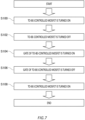
- Fig. 7 shows an example of a flowchart of a control method of a silicon carbide MOSFET inverter circuit 100.
- the present example shows an example of a flowchart of a control method of a silicon carbide MOSFET inverter circuit 100, but not limited thereto.
- a gate of the to-be-controlled MOSFET is turned on. In this manner, a synchronization control of the to-be-controlled MOSFET 20 is started.
- the gate of the to-be-controlled MOSFET 20 may be turned on such that the saturation current period is 2 ⁇ s
- the gate of the to-be-controlled MOSFET 20 may be turned on such that the saturation current period is 3 ⁇ s
- the gate of the to-be-controlled MOSFET 20 may be turned on such that the saturation current period is 4 ⁇ s
- the gate of the to-be-controlled MOSFET 20 may be turned on such that the saturation current period is less than 5 ⁇ s.
- the current density of the transient current flowing in the built-in diode of the to-be-controlled MOSFET 20 may be less than 1000A/cm 2 . That is, the current density of the saturation current Ic may be less than 1000A/cm 2 . As an example, the current density of the saturation current Ic is 900A/cm 2 .
- an expansion of stacking faults of the to-be-controlled MOSFET 20 can be suppressed. That is, by performing the synchronization control on the to-be-controlled MOSFET 20 to cause the saturation current period in which the transient current becomes the saturation current Ic to be less than 5 ⁇ s, the current flowing in the built-in diode during a period in which an amount of holes injected in the to-be-controlled MOSFET 20 is small can be reduced, and the frequency of recombining the electrons and the holes can be reduced to suppress the expansion of the stacking faults.
- the synchronization control of the to-be-controlled MOSFET 20 ends.
- the to-be-controlled MOSFET 20 may be operated repeatedly by periodically repeating the step S100 to S108. That is, S100 and S108 may indicate the same step.
Landscapes
- Engineering & Computer Science (AREA)
- Power Engineering (AREA)
- Electrodes Of Semiconductors (AREA)
Applications Claiming Priority (2)
| Application Number | Priority Date | Filing Date | Title |
|---|---|---|---|
| JP2022201584 | 2022-12-16 | ||
| PCT/JP2023/038187 WO2024127817A1 (ja) | 2022-12-16 | 2023-10-23 | 炭化珪素mosfetインバータ回路および炭化珪素mosfetインバータ回路の制御方法 |
Publications (2)
| Publication Number | Publication Date |
|---|---|
| EP4517833A1 true EP4517833A1 (de) | 2025-03-05 |
| EP4517833A4 EP4517833A4 (de) | 2026-02-18 |
Family
ID=91485439
Family Applications (1)
| Application Number | Title | Priority Date | Filing Date |
|---|---|---|---|
| EP23903116.4A Pending EP4517833A4 (de) | 2022-12-16 | 2023-10-23 | Siliciumcarbid-mosfet-wechselrichterschaltung und verfahren zur steuerung einer siliciumcarbid-mosfet-wechselrichterschaltung |
Country Status (5)
| Country | Link |
|---|---|
| US (1) | US20250088120A1 (de) |
| EP (1) | EP4517833A4 (de) |
| JP (1) | JPWO2024127817A1 (de) |
| CN (1) | CN119278577A (de) |
| WO (1) | WO2024127817A1 (de) |
Family Cites Families (17)
| Publication number | Priority date | Publication date | Assignee | Title |
|---|---|---|---|---|
| EP1353385B1 (de) * | 2001-01-19 | 2014-09-24 | Mitsubishi Denki Kabushiki Kaisha | Halbleiteranordnung |
| JP5374883B2 (ja) * | 2008-02-08 | 2013-12-25 | 富士電機株式会社 | 半導体装置およびその製造方法 |
| JP2013145770A (ja) * | 2012-01-13 | 2013-07-25 | Sumitomo Electric Ind Ltd | 半導体装置およびその製造方法 |
| WO2016002766A1 (ja) * | 2014-06-30 | 2016-01-07 | 国立研究開発法人産業技術総合研究所 | 炭化珪素半導体装置およびその製造方法 |
| JP6167244B2 (ja) * | 2014-08-27 | 2017-07-19 | 株式会社日立製作所 | 電力変換装置、モータ装置および逆変換器モジュール |
| WO2017043607A1 (ja) * | 2015-09-09 | 2017-03-16 | 住友電気工業株式会社 | 縦型炭化珪素半導体装置のトレンチのアニール処理装置、縦型炭化珪素半導体装置の製造方法および縦型炭化珪素半導体装置 |
| US9595958B1 (en) | 2015-09-11 | 2017-03-14 | Fuji Electric Co., Ltd. | Semiconductor device and driving method for the same |
| JP2017112161A (ja) * | 2015-12-15 | 2017-06-22 | 三菱電機株式会社 | 半導体装置 |
| JP6711100B2 (ja) * | 2016-04-15 | 2020-06-17 | 富士電機株式会社 | 炭化珪素半導体装置、炭化珪素半導体装置の製造方法および炭化珪素半導体装置の制御方法 |
| JP6863464B2 (ja) * | 2017-09-05 | 2021-04-21 | 富士電機株式会社 | 炭化珪素半導体装置および炭化珪素半導体装置の製造方法 |
| JP6977469B2 (ja) * | 2017-10-18 | 2021-12-08 | 富士電機株式会社 | 炭化珪素mosfetインバータ回路 |
| JP7052330B2 (ja) * | 2017-12-13 | 2022-04-12 | 富士電機株式会社 | 絶縁ゲート型半導体装置及びその製造方法 |
| JP7167533B2 (ja) * | 2018-08-03 | 2022-11-09 | 富士電機株式会社 | 半導体装置および半導体回路装置 |
| JP7151363B2 (ja) * | 2018-10-16 | 2022-10-12 | 富士電機株式会社 | 炭化珪素半導体装置および炭化珪素半導体装置の製造方法 |
| CN112335057B (zh) * | 2018-12-04 | 2024-06-28 | 住友电气工业株式会社 | 碳化硅外延衬底及碳化硅半导体器件 |
| JP7302286B2 (ja) * | 2019-05-23 | 2023-07-04 | 富士電機株式会社 | 半導体装置 |
| CN115917756A (zh) * | 2020-12-24 | 2023-04-04 | 富士电机株式会社 | 绝缘栅型半导体装置 |
-
2023
- 2023-10-23 EP EP23903116.4A patent/EP4517833A4/de active Pending
- 2023-10-23 WO PCT/JP2023/038187 patent/WO2024127817A1/ja not_active Ceased
- 2023-10-23 CN CN202380042568.7A patent/CN119278577A/zh active Pending
- 2023-10-23 JP JP2024564195A patent/JPWO2024127817A1/ja active Pending
-
2024
- 2024-11-24 US US18/957,822 patent/US20250088120A1/en active Pending
Also Published As
| Publication number | Publication date |
|---|---|
| CN119278577A (zh) | 2025-01-07 |
| EP4517833A4 (de) | 2026-02-18 |
| WO2024127817A1 (ja) | 2024-06-20 |
| JPWO2024127817A1 (de) | 2024-06-20 |
| US20250088120A1 (en) | 2025-03-13 |
Similar Documents
| Publication | Publication Date | Title |
|---|---|---|
| CN111418071B (zh) | 半导体装置以及功率变换装置 | |
| US6388287B2 (en) | Switch mode power supply with reduced switching losses | |
| EP0899791B1 (de) | Grabengate-MOSFET mit bidirektionalem Spannungsclamping | |
| US5828100A (en) | Insulated gate semiconductor device having trench gate and inverter provided with the same | |
| US11063122B2 (en) | Silicon carbide semiconductor device and power conversion device | |
| US20080258172A1 (en) | Insulated gate bipolar transistor with built-in freewheeling diode | |
| JP2009033036A (ja) | 半導体装置及びこれを用いた電気回路装置 | |
| US11894428B2 (en) | Silicon carbide semiconductor device and power converter | |
| US20230139229A1 (en) | Semiconductor device and power converter | |
| EP2811632A1 (de) | Treiberschaltung für halbleiterschaltelement und leistungswandlerschaltung damit | |
| CN111466032A (zh) | 碳化硅半导体装置以及电力变换装置 | |
| JP6652802B2 (ja) | 半導体装置、および当該半導体装置を備えるインバータ装置 | |
| US11588048B2 (en) | Semiconductor device with insulated gate transistor cell and rectifying junction | |
| US20060071280A1 (en) | Semiconductor diode, electronic component, voltage source inverter and control method | |
| JP2019106409A (ja) | 半導体装置およびその製造方法 | |
| JP2020077721A (ja) | 炭化珪素半導体装置および電力変換装置 | |
| JP2023147422A (ja) | 半導体装置および電力変換装置 | |
| EP4517833A1 (de) | Siliciumcarbid-mosfet-wechselrichterschaltung und verfahren zur steuerung einer siliciumcarbid-mosfet-wechselrichterschaltung | |
| EP1713128B1 (de) | IGBT und diesen verwendende elektrische Stromwandlungsvorrichtung | |
| US10186571B2 (en) | Power semiconductor device and method therefor | |
| JP2023144460A (ja) | 半導体装置、半導体装置および電力変換装置 | |
| EP0691687A2 (de) | Vertikales MOS-Halbleiterbauelement | |
| EP0977271B1 (de) | Halbleiter-IGBT-Modul | |
| US20250311396A1 (en) | Power conversion device, method of controlling power conversion device, semiconductor device, and method of controlling semiconductor device | |
| EP4105989A1 (de) | Halbleiterbauelement mit einer mit der gate-metallisierung verbundenen diodenkette |
Legal Events
| Date | Code | Title | Description |
|---|---|---|---|
| STAA | Information on the status of an ep patent application or granted ep patent |
Free format text: STATUS: THE INTERNATIONAL PUBLICATION HAS BEEN MADE |
|
| PUAI | Public reference made under article 153(3) epc to a published international application that has entered the european phase |
Free format text: ORIGINAL CODE: 0009012 |
|
| STAA | Information on the status of an ep patent application or granted ep patent |
Free format text: STATUS: REQUEST FOR EXAMINATION WAS MADE |
|
| 17P | Request for examination filed |
Effective date: 20241125 |
|
| AK | Designated contracting states |
Kind code of ref document: A1 Designated state(s): AL AT BE BG CH CY CZ DE DK EE ES FI FR GB GR HR HU IE IS IT LI LT LU LV MC ME MK MT NL NO PL PT RO RS SE SI SK SM TR |
|
| REG | Reference to a national code |
Ref country code: DE Ref legal event code: R079 Free format text: PREVIOUS MAIN CLASS: H01L0029780000 Ipc: H10D0030660000 |
|
| A4 | Supplementary search report drawn up and despatched |
Effective date: 20260119 |
|
| RIC1 | Information provided on ipc code assigned before grant |
Ipc: H10D 30/66 20250101AFI20260113BHEP Ipc: H03K 17/08 20060101ALI20260113BHEP Ipc: H03K 17/28 20060101ALI20260113BHEP |
|
| DAV | Request for validation of the european patent (deleted) | ||
| DAX | Request for extension of the european patent (deleted) |