EP4517809A1 - Halbleiterbauelement und herstellungsverfahren dafür - Google Patents
Halbleiterbauelement und herstellungsverfahren dafür Download PDFInfo
- Publication number
- EP4517809A1 EP4517809A1 EP23818976.5A EP23818976A EP4517809A1 EP 4517809 A1 EP4517809 A1 EP 4517809A1 EP 23818976 A EP23818976 A EP 23818976A EP 4517809 A1 EP4517809 A1 EP 4517809A1
- Authority
- EP
- European Patent Office
- Prior art keywords
- dielectric layer
- groove
- semiconductor component
- preparation
- layer
- Prior art date
- Legal status (The legal status is an assumption and is not a legal conclusion. Google has not performed a legal analysis and makes no representation as to the accuracy of the status listed.)
- Pending
Links
Images

Classifications
-
- H—ELECTRICITY
- H10—SEMICONDUCTOR DEVICES; ELECTRIC SOLID-STATE DEVICES NOT OTHERWISE PROVIDED FOR
- H10D—INORGANIC ELECTRIC SEMICONDUCTOR DEVICES
- H10D30/00—Field-effect transistors [FET]
- H10D30/40—FETs having zero-dimensional [0D], one-dimensional [1D] or two-dimensional [2D] charge carrier gas channels
- H10D30/47—FETs having zero-dimensional [0D], one-dimensional [1D] or two-dimensional [2D] charge carrier gas channels having two-dimensional [2D] charge carrier gas channels, e.g. nanoribbon FETs or high electron mobility transistors [HEMT]
- H10D30/471—High electron mobility transistors [HEMT] or high hole mobility transistors [HHMT]
- H10D30/475—High electron mobility transistors [HEMT] or high hole mobility transistors [HHMT] having wider bandgap layer formed on top of lower bandgap active layer, e.g. undoped barrier HEMTs such as i-AlGaN/GaN HEMTs
-
- H—ELECTRICITY
- H10—SEMICONDUCTOR DEVICES; ELECTRIC SOLID-STATE DEVICES NOT OTHERWISE PROVIDED FOR
- H10D—INORGANIC ELECTRIC SEMICONDUCTOR DEVICES
- H10D30/00—Field-effect transistors [FET]
- H10D30/01—Manufacture or treatment
- H10D30/015—Manufacture or treatment of FETs having heterojunction interface channels or heterojunction gate electrodes, e.g. HEMT
-
- H—ELECTRICITY
- H10—SEMICONDUCTOR DEVICES; ELECTRIC SOLID-STATE DEVICES NOT OTHERWISE PROVIDED FOR
- H10W—GENERIC PACKAGES, INTERCONNECTIONS, CONNECTORS OR OTHER CONSTRUCTIONAL DETAILS OF DEVICES COVERED BY CLASS H10
- H10W74/00—Encapsulations, e.g. protective coatings
- H10W74/10—Encapsulations, e.g. protective coatings characterised by their shape or disposition
- H10W74/131—Encapsulations, e.g. protective coatings characterised by their shape or disposition the semiconductor body being only partially enclosed
- H10W74/137—Encapsulations, e.g. protective coatings characterised by their shape or disposition the semiconductor body being only partially enclosed the encapsulations being directly on the semiconductor body
-
- H—ELECTRICITY
- H10—SEMICONDUCTOR DEVICES; ELECTRIC SOLID-STATE DEVICES NOT OTHERWISE PROVIDED FOR
- H10D—INORGANIC ELECTRIC SEMICONDUCTOR DEVICES
- H10D62/00—Semiconductor bodies, or regions thereof, of devices having potential barriers
- H10D62/80—Semiconductor bodies, or regions thereof, of devices having potential barriers characterised by the materials
- H10D62/85—Semiconductor bodies, or regions thereof, of devices having potential barriers characterised by the materials being Group III-V materials, e.g. GaAs
- H10D62/8503—Nitride Group III-V materials, e.g. AlN or GaN
Definitions
- This application relates to the field of semiconductor technologies, and in particular, to a semiconductor component, an electronic chip, an electronic device, and a preparation method for a semiconductor component.
- the semiconductor component may include a substrate, an epitaxial layer, a dielectric layer, and the like that are stacked.
- the substrate may include elements such as silicon, arsenic, and carbon
- the epitaxial layer may include elements such as gallium, nitrogen, and aluminum
- the dielectric layer may include elements such as silicon, oxygen, and nitrogen.
- a material included in the dielectric layer determines insulation of the dielectric layer, and further affects static power consumption of the semiconductor component.
- This application provides a semiconductor component, an electronic chip, an electronic device, and a preparation method for a semiconductor component, to improve insulation of a first dielectric layer, reduce a static current of the semiconductor component, and therefore reduce static power consumption of the semiconductor component.
- this application provides a semiconductor component.
- the semiconductor component may include a substrate, an epitaxial layer, a first dielectric layer, and a second dielectric layer.
- the substrate, the epitaxial layer, the first dielectric layer, and the second dielectric layer may be sequentially stacked.
- an element included in the first material may not be completely the same as an element included in the second material. That is, the element included in the first material may be partially the same as or completely different from the element included in the second material.
- the element included in the first material included in the first dielectric layer is not completely the same as the element included in the second material included in the second dielectric layer, the first dielectric layer includes the first material including the aluminum element, and the second dielectric layer includes the second material including the silicon element.
- This can increase a relative dielectric constant (which may also be referred to as relative permittivity) of the first dielectric layer, thereby improving insulation of the first dielectric layer, reducing a static current of the semiconductor component, and reducing static power consumption of the semiconductor component.
- an element included in a material included in the epitaxial layer may not be completely the same as an element included in a material included in the substrate. That is, the element included in the material included in the epitaxial layer may be partially or completely different from the element included in the material included in the substrate. Therefore, the epitaxial layer may be referred to as heteroepitaxy.
- the passive component may include a resistor, a capacitor, and the like.
- the passive component is not limited in this application.
- this application provides an electronic device.
- the electronic device may include a circuit board and the electronic chip provided in the second aspect and the possible implementation of the second aspect.
- the electronic chip may be disposed on the circuit board.
- this application provides a preparation method for a semiconductor component.
- the semiconductor component may include a substrate, an epitaxial layer, a first dielectric layer, and a second dielectric layer that are sequentially stacked.
- the preparation method may include: performing photoetching on the second dielectric layer, to form a mask layer; etching the second dielectric layer based on the mask layer, and removing the mask layer, to form a first groove; and etching the first dielectric layer based on the first groove, to form a second groove.
- an element included in the first material may not be completely the same as an element included in the second material. That is, the element included in the first material may be partially the same as or completely different from the element included in the second material.
- the first material may include an aluminum element
- the second material may include a silicon element
- the performing photoetching on the second dielectric layer, to form a mask layer may include: coating a surface of the second dielectric layer with photoresist, and baking, based on preset baking temperature and preset baking time, the second dielectric layer coated with the photoresist; exposing the baked second dielectric layer based on preset exposure time; and developing the exposed second dielectric layer based on preset development time by using a developer, to form the mask layer.
- the preset baking temperature may be 90°C to 120°C, and the preset baking time may be 3 min to 5 min.
- the preset baking temperature may alternatively be within another temperature range, and the preset baking time may alternatively be within another time range. This is not limited in this application.
- the preset exposure time may be 100 ms to 300 ms, and the preset development time may be 40s to 70s.
- the preset exposure time and the preset development time each may alternatively be within another time range. This is not limited in this application.
- the developer may be tetramethylammonium hydroxide.
- the developer may alternatively be of another type. This is not limited in this application.
- the etching the second dielectric layer based on the mask layer, and removing the mask layer, to form a first groove may include: etching the second dielectric layer based on the mask layer by using a dry etching process, to obtain the etched second dielectric layer; and removing the mask layer on the surface of the etched second dielectric layer by using a photoresist remover, to form the first groove. That is, the photoresist is used as the mask layer, and the second dielectric layer is etched by using the dry etching process. It can be learned that, in this application, the second dielectric layer is etched by using the dry etching process, to form the first groove.
- a depth of the first groove is an etching depth of the second dielectric layer, and does not include a thickness of the mask layer on the surface of the etched second dielectric layer.
- the second dielectric layer is etched by using the dry etching process, so that the depth of the first groove can be accurately controlled, thereby improving uniformity and a yield rate of the semiconductor component.
- fluorine-based gas or chlorine-based gas may be selected, to etch the second dielectric layer by using the dry etching process.
- the fluorine-based gas may be gas including a fluorine element, a carbon element, a sulfur element, and the like, such as sulfur hexafluoride, carbon tetrafluoride, trifluoromethane, hexafluoroethane, or perfluoropropane.
- the chlorine-based gas may be gas including a chlorine element, such as carbon tetrachloride, chlorine gas, or boron chloride.
- the dry etching process may be any one of a reactive ion etching (reactive ion etching, RIE) process (an RIE process for short), an inductively coupled plasma (inductively coupled plasma, ICP) etching process (an ICP process for short), an advanced oxide etching (advanced oxide etching, AOE) process (an AOE process for short), and the like.
- RIE reactive ion etching
- ICP inductively coupled plasma
- AOE advanced oxide etching
- the second dielectric layer may alternatively be etched by using another dry etching process. This is not limited in this application.
- the mask layer on the surface of the etched second dielectric layer is removed by using the photoresist remover, and the mask layer on the surface of the etched second dielectric layer may be cleaned by using different photoresist removers, to form the first groove.
- the photoresist remover may include any one of acetone, isopropyl alcohol, ethanol absolute, and N-methylpyrrolidone.
- the photoresist remover may alternatively include a combination of at least two of acetone, isopropyl alcohol, ethanol absolute, and N-methylpyrrolidone.
- the etching the first dielectric layer based on the first groove, to form a second groove may include: etching the first dielectric layer based on the first groove by using a wet corrosion process, to form the second groove.
- the first dielectric layer at a bottom of the first groove is etched based on the first groove, to obtain the second groove.
- the depth of the first groove may be the etching depth of the second dielectric layer
- a depth of the second groove may be a sum of the etching depth of the second dielectric layer and the corrosion depth of the first dielectric layer. Therefore, the depth of the second groove may be greater than the depth of the first groove.
- the first dielectric layer may be etched based on the first groove and preset corrosion time by using a corrosion solution, to form the second groove. That is, in this application, the first dielectric layer may be etched by using the wet corrosion process, to form the second groove.
- the corrosion solution includes any one of a solution prepared from sulfuric acid and hydrogen peroxide according to a preset ratio, a tetramethylammonium hydroxide solution, and a potassium hydroxide solution.
- the corrosion solution may alternatively be another solution that can etch the first dielectric layer. This is not limited in this application.
- the preset corrosion time may be 1 min to 20 min. Certainly, the preset corrosion time may alternatively be within another time range. This is not limited in this application.
- the first dielectric layer is etched by using the wet corrosion process.
- damage to an interface of the second groove is avoided, an interface state of a gate (which means some discrete or continuous electronic energy states or energy bands whose energy values are in a band gap at an interface between the gate and the epitaxial layer) is reduced, and gate leakage is avoided, thereby improving reliability of the semiconductor component.
- the first material may be aluminum oxide or aluminum nitride.
- the second material may be silicon oxide, silicon nitride, or silicon oxynitride.
- the first material may alternatively be another material including an aluminum element, and the second material may alternatively be another material including a silicon element. This is not limited in this application.
- the second dielectric layer may not include the aluminum element. That is, the first dielectric layer may include the aluminum element, the second dielectric layer may include the silicon element, but the second dielectric layer may not include the aluminum element.
- a thickness of the first dielectric layer may be 5 nm to 30 nm.
- a thickness of the second dielectric layer may be 100 nm to 300 nm.
- the thickness of the first dielectric layer and the thickness of the second dielectric layer each may be within another thickness range. This is not limited in this application.
- the dry etching process and the wet corrosion process are combined, the first groove is formed by using the dry etching process, and the second groove used to deposit the gate is formed by using the wet corrosion process.
- the depth of the first groove can be accurately controlled, thereby improving the uniformity and the yield rate of the semiconductor component.
- the damage to the interface of the second groove can be avoided, the interface state of the gate can be reduced, and the gate leakage can be avoided, thereby improving the reliability of the semiconductor component.
- this application provides a preparation method for a semiconductor component.
- the semiconductor component may include a substrate, an epitaxial layer, a first dielectric layer, and a second dielectric layer that are sequentially stacked.
- the preparation method may include: forming the epitaxial layer on a surface of the substrate; forming the first dielectric layer on a surface of the epitaxial layer by using a first material; and forming the second dielectric layer on a surface of the first dielectric layer by using a second material.
- the first dielectric layer may include the first material
- the second dielectric layer may include the second material
- an element included in the first material may not be completely the same as an element included in the second material. That is, the element included in the first material may be partially the same as or completely different from the element included in the second material.
- the first material may include an aluminum element
- the second material may include a silicon element
- the first material may be aluminum oxide or aluminum nitride.
- the second material may be silicon oxide, silicon nitride, or silicon oxynitride.
- the first material may alternatively be another material including an aluminum element, and the second material may alternatively be another material including a silicon element. This is not limited in this application.
- the second dielectric layer may not include the aluminum element. That is, the first dielectric layer may include the aluminum element, the second dielectric layer may include the silicon element, but the second dielectric layer may not include the aluminum element.
- a thickness of the first dielectric layer may be 5 nm to 30 nm.
- a thickness of the second dielectric layer may be 100 nm to 300 nm.
- the thickness of the first dielectric layer and the thickness of the second dielectric layer each may be within another thickness range. This is not limited in this application.
- At least one (item) means one or more, and "a plurality of” means two or more.
- the term “and/or” is used for describing an association relationship between associated objects, and represents that three relationships may exist.
- a and/or B may represent the following three cases: Only A exists, only B exists, and both A and B exist, where A and B may be singular or plural.
- the character “/” generally indicates an "or” relationship between the associated objects.
- At least one item (piece) of the following” or a similar expression thereof means any combination of these items, including a singular item (piece) or any combination of plural items (pieces).
- At least one item (piece) of a, b, or c may indicate: a, b, c, a and b, a and c, b and c, or a, b, and c, where a, b, and c may be singular or plural.
- the semiconductor component may include a substrate, an epitaxial layer, a dielectric layer, and the like that are stacked.
- the substrate may include elements such as silicon Si (silicon), arsenic As (arsenic), and carbon C (carbon).
- the epitaxial layer may include elements such as gallium Ga (gallium), nitrogen N (nitrogen), and aluminum Al (aluminum).
- the dielectric layer may include elements such as silicon, oxygen O (oxygen), and nitrogen.
- a material included in the dielectric layer determines insulation of the dielectric layer, and further affects static power consumption of the semiconductor component.
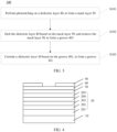
- the semiconductor component 1 may include a substrate 10, an epitaxial layer 20, a dielectric layer 30 (namely a first dielectric layer), and a dielectric layer 40 (namely a second dielectric layer).
- the substrate 10, the epitaxial layer 20, the dielectric layer 30, and the dielectric layer 40 may be sequentially stacked.
- the dielectric layer 30 may include a material A (namely a first material), and the dielectric layer 40 may include a material B (namely a second material).
- an element included in the material A may not be completely the same as an element included in the material B. That is, the element included in the material A may be partially the same as or completely different from the element included in the material B.
- the material A may include an aluminum element
- the material B may include a silicon element
- the element included in the material A included in the dielectric layer 30 is not completely the same as the element included in the material B included in the dielectric layer 40.
- the dielectric layer 30 includes the material A including the aluminum element, so that a relative dielectric constant of the dielectric layer 30 can be increased, thereby improving insulation of the dielectric layer 30, reducing a static current of the semiconductor component 1, and reducing static power consumption of the semiconductor component 1.
- the dielectric layer 40 includes the material B including the silicon element.
- a groove 301 (namely a second groove) may be provided on each of the dielectric layer 30 and the dielectric layer 40.
- a depth of the groove 301 may be a sum of a thickness of the dielectric layer 30 (namely an etching depth of the dielectric layer 30 below) and a thickness of the dielectric layer 40 (namely a corrosion depth of the dielectric layer 40 below).
- the groove 301 is used to form a gate of the semiconductor component 1. Refer to the following descriptions.
- an element included in a material included in the epitaxial layer 20 may not be completely the same as an element included in a material included in the substrate 10. That is, the element included in the material included in the epitaxial layer 20 may be partially or completely different from the element included in the material included in the substrate 10. Therefore, the epitaxial layer 20 may be referred to as heteroepitaxy.
- the epitaxial layer 20 may include a buffer layer 201, a channel layer 202, an insertion layer 203, a barrier layer 204, and a cap layer 205 that are sequentially stacked.
- the buffer layer 201 is in contact with the substrate 10, and the cap layer 205 is in contact with the dielectric layer 30.
- the substrate 10 may include silicon, silicon carbide SiC (silicon carbide), sapphire (sapphire), and the like.
- the buffer layer 201 may include a material like gallium nitride GaN (gallium nitride) or aluminum nitride AlN (aluminum nitride).
- the channel layer 202 may include a material like the gallium nitride GaN.
- the insertion layer 203 may include a material like the aluminum nitride AlN.
- the barrier layer 204 may include a material like aluminum gallium nitride AlGaN (aluminum gallium nitride) or indium aluminum nitride InAlN (indium aluminum nitride).
- the cap layer 205 may include a material like the gallium nitride GaN.
- the buffer layer 201, the channel layer 202, the insertion layer 203, the barrier layer 204, and the cap layer 205 each may alternatively include another material. This is not limited in this embodiment of this application.
- the substrate 10 may include the silicon Si
- the buffer layer 201, the channel layer 202, and the cap layer 205 may include the gallium nitride GaN
- the insertion layer 203 may include the aluminum nitride AlN
- the barrier layer 204 may include the aluminum gallium nitride AlGaN. Therefore, the element included in the material included in the epitaxial layer 20 is completely different from the element included in the material included in the substrate 10.
- the epitaxial layer 20 in this embodiment of this application is the heteroepitaxy.
- the semiconductor component 1 may further include a gate dielectric layer 60, a source 90, a gate 70, and a drain 80, as shown in FIG. 2 .
- the gate dielectric layer 60 may be stacked on a surface of the dielectric layer 40 and inside the groove 301.
- the gate 70 may be disposed on a surface of the gate dielectric layer 60.
- the source 90 and the drain 80 may also be disposed on the surface of the gate dielectric layer 60.
- the source 90 may pass through the dielectric layer 30 and the dielectric layer 40 to be in contact with the cap layer 205.
- the drain 80 may also pass through the dielectric layer 30 and the dielectric layer 40 to be in contact with the cap layer 205. Therefore, ohmic contact may be formed between the source 90 and the cap layer 205, and ohmic contact may also be formed between the drain 80 and the cap layer 205.
- the material A may be aluminum oxide or aluminum nitride.
- the material B may be silicon oxide, silicon nitride, or silicon oxynitride.
- the material A may alternatively be another material including the aluminum element, and the material B may alternatively be another material including the silicon element. This is not limited in this application.
- the dielectric layer 40 may not include the aluminum element. That is, the dielectric layer 30 may include the aluminum element, the dielectric layer 40 may include the silicon element, but the dielectric layer 40 may not include the aluminum element.
- the dielectric layer 30 may include aluminum oxide Al 2 O 3 (aluminum oxide), and the dielectric layer 40 may include silicon dioxide SiO 2 .
- the thickness of the dielectric layer 30 may be 5 nm to 30 nm.
- the thickness of the dielectric layer 40 may be 100 nm to 300 nm.
- the dielectric layer 30 and the dielectric layer 40 each may be within another thickness range. This is not limited in this application.
- the thickness of the dielectric layer 30 may be 25 nm, and the thickness of the dielectric layer 40 may be 200 nm.
- the semiconductor component 1 provided in this embodiment of this application may be a field-effect transistor, and may further be a high electron mobility transistor (high electron mobility transistor, HEMT), a heterojunction field effect transistor (heterojunction field effect transistor, HFET), or a modulation-doped field-effect transistor (modulation-doped FET, MODFET).
- HEMT high electron mobility transistor
- HFET heterojunction field effect transistor
- MODFET modulation-doped field-effect transistor
- An embodiment of this application further provides an electronic chip.
- the electronic chip may include a passive component and a semiconductor component 1.
- the passive component may be electrically connected to the semiconductor component 1.
- the passive component may include a resistor, a capacitor, and the like.
- the passive component is not limited in this embodiment of this application.
- An embodiment of this application further provides an electronic device.
- the electronic device may include a circuit board and the foregoing electronic chip.
- the electronic chip may be disposed on the circuit board.
- An embodiment of this application provides a preparation method for a semiconductor component.
- the semiconductor component For related descriptions of the semiconductor component, refer to the foregoing descriptions. Details are not described in this embodiment of this application again.
- a process 100 may be implemented based on the following steps.
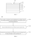
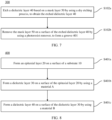
- Step S101 Perform photoetching on a dielectric layer 40, to form a mask layer 50, as shown in FIG. 4 .
- Step S102 Etch the dielectric layer 40 based on the mask layer 50, and remove the mask layer 50, to form a groove 401, as shown in FIG. 5 .
- a depth of the groove 401 may be an etching depth of the dielectric layer 40, and does not include a thickness of the mask layer 50 on a surface of the etched dielectric layer 40, that is, does not include the thickness of the mask layer 50 in FIG. 4 .
- Step S103 Etch a dielectric layer 30 based on the groove 401, to form a groove 301, as shown in FIG. 1 .
- step S101 may be implemented based on the following steps.
- Step S101a Coat the surface of the dielectric layer 40 with photoresist, and bake, based on preset baking temperature and preset baking time, the dielectric layer 40 coated with the photoresist.
- the photoresist may be positive photoresist or negative photoresist.
- the photoresist in an exposure area may be dissolved, that is, the positive photoresist is developed in the exposure area.
- the photoresist in a non-exposure area may be dissolved, that is, the negative photoresist is developed in the non-exposure area.
- the surface of the dielectric layer 40 is coated with the positive photoresist.
- the preset baking temperature may be 90°C to 120°C, and the preset baking time may be 3 min to 5 min.
- the preset baking temperature may alternatively be within another temperature range, and the preset baking time may alternatively be within another time range. This is not limited in this application. In this embodiment of this application, the preset baking temperature may be 100°C, and the preset baking time may be 4 min.
- Step S101b Expose the baked dielectric layer 40 based on preset exposure time.
- the preset exposure time may be 100 ms to 300 ms. Certainly, the preset exposure time may alternatively be within another time range. This is not limited in this application. In this embodiment of this application, the preset exposure time may be 110 ms.
- Step S101c Develop the exposed dielectric layer 40 based on preset development time by using a developer, to form the mask layer 50, as shown in FIG. 4 .
- the preset development time may be 40s to 70s. Certainly, the preset development time may alternatively be within another time range. This is not limited in this application. In this embodiment of this application, the preset development time may be 50s.
- the developer may be tetramethylammonium hydroxide C 4 H 13 NO (tetramethylammonium hydroxide).
- the developer may alternatively be of another type. This is not limited in this application.
- the mask layer 50 may alternatively be formed in another manner. This is not limited in this embodiment of this application.
- reactive gas such as a reactive ion (reactive ion, RI), inductively coupled plasma (inductively coupled plasma, ICP), or an ion beam (ion beam, IB)
- reactive gas such as a reactive ion (reactive ion, RI), inductively coupled plasma (inductively coupled plasma, ICP), or an ion beam (ion beam, IB)
- RI reactive ion
- ICP inductively coupled plasma
- IB ion beam
- the photoresist may be used as the mask layer 50, and the dielectric layer 40 is etched by using the dry etching process.
- step S102 may be implemented based on the following steps.
- Step S102a Etch the dielectric layer 40 based on the mask layer 50 by using the dry etching process, to obtain the etched dielectric layer 40.
- Step S102b Remove the mask layer 50 on the surface of the etched dielectric layer 40 by using a photoresist remover, to form the groove 401, as shown in FIG. 5 .
- fluorine-based gas or chlorine-based gas may be selected, to etch the dielectric layer 40 using the dry etching process based on preset etching time.
- the fluorine-based gas may be gas including a fluorine element, a carbon element, a sulfur element, and the like, such as sulfur hexafluoride, carbon tetrafluoride, trifluoromethane, hexafluoroethane, or perfluoropropane.
- the chlorine-based gas may be gas including a chlorine element, such as carbon tetrachloride, chlorine gas, or boron chloride.
- the etching time may be a ratio of a thickness of the dielectric layer 40 to an etching rate.
- the dry etching process may be any one of a reactive ion etching (reactive ion etching, RIE) process (an RIE process for short), an inductively coupled plasma (inductively coupled plasma, ICP) etching process (an ICP process for short), an advanced oxide etching (advanced oxide etching, AOE) process (an AOE process for short), and the like.
- RIE reactive ion etching
- ICP inductively coupled plasma
- AOE advanced oxide etching
- the dielectric layer 40 may alternatively be etched by using another dry etching process. This is not limited in this application.
- the carbon tetrafluoride is selected, to etch the dielectric layer 40 by using the AOE process.
- the etching time is 1 min, and the etching depth of the dielectric layer 40 is 210 nm. It may be understood that the depth of the groove 401 is 210 nm.
- the mask layer 50 on the surface of the etched dielectric layer 40 may be cleaned by using different photoresist removers, to form the groove 401.
- the photoresist remover may include any one of acetone CH 3 COCH 3 (acetone), isopropyl alcohol C 3 H 8 O (isopropyl alcohol, IPA), ethanol absolute C 2 H 6 O (ethanol absolute), and N-methylpyrrolidone C 5 H 9 NO (N-methylpyrrolidone).
- the photoresist remover may alternatively include a combination of at least two of acetone, isopropyl alcohol, ethanol absolute, and N-methylpyrrolidone.
- the mask layer 50 on the surface of the etched dielectric layer 40 is cleaned by using the acetone and the isopropyl alcohol.
- the mask layer 50 on the surface of the etched dielectric layer 40 is removed, so that impact on a corrosion rate and a corrosion depth of the dielectric layer 30 can be avoided, thereby improving reliability of the preparation method.
- the groove 401 may alternatively be formed in another manner. This is not limited in this embodiment of this application.
- the dielectric layer 40 is etched by using the dry etching process, so that the depth of the groove 401 can be accurately controlled, thereby improving uniformity and a yield rate of the semiconductor component 1.
- a wet corrosion process is a process of etching a dielectric layer by using a corrosion solution.
- the dielectric layer 30 may be etched based on the groove 401 and preset corrosion time by using a corrosion solution, to form the groove 301. That is, in this embodiment of this application, the groove 301 is formed by using the wet corrosion process, as shown in FIG. 1 .
- the corrosion solution may include any one of a solution prepared from sulfuric acid H 2 SO 4 (sulfuric acid) and hydrogen peroxide H 2 O 2 (hydrogen peroxide) according to a preset ratio, a tetramethylammonium hydroxide C 4 H 13 NO (tetramethylammonium hydroxide, TMAH) solution, and a potassium hydroxide KOH (potassium hydroxide) solution.
- the corrosion solution may alternatively be another solution that can etch the dielectric layer 30. This is not limited in this embodiment of this application.
- the corrosion solution is the solution prepared from the sulfuric acid whose mass fraction is greater than or equal to 70% (namely concentrated sulfuric acid) and the hydrogen peroxide.
- the preset ratio is a volume ratio of the concentrated sulfuric acid to the hydrogen peroxide, and may be 7:3.
- the preset corrosion time may be 1 min to 20 min. Certainly, the preset corrosion time may alternatively be within another time range. This is not limited in this application. In this embodiment of this application, the preset corrosion time may be 5 min.
- the groove 301 may alternatively be formed in another manner. This is not limited in this embodiment of this application.
- the dielectric layer 30 is etched by using the wet corrosion process. In this way, damage to an interface of the groove 301 is avoided, an interface state of a gate (which means some discrete or continuous electronic energy states or energy bands whose energy values are in a band gap at an interface between the gate and the epitaxial layer) is reduced, and gate leakage is avoided, thereby improving reliability of the semiconductor component.
- a gate which means some discrete or continuous electronic energy states or energy bands whose energy values are in a band gap at an interface between the gate and the epitaxial layer
- the dielectric layer 30 and the dielectric layer 40 may be further formed based on the following steps.
- Step S401b Form the dielectric layer 30 on a surface of the epitaxial layer 20 by using a material A.
- Step S401c Form the dielectric layer 40 on a surface of the dielectric layer 30 by using a material B.
- the dielectric layer 30 may be formed on the surface of the epitaxial layer 20 by using a deposition process.
- the deposition process may include an atomic layer deposition (atomic layer deposition, ALD) process (an ALD process for short), a plasma enhanced atomic layer deposition (plasma enhanced atomic layer deposition, PEALD) process (a PEALD process for short), a plasma enhanced chemical vapor deposition (plasma enhanced chemical vapor deposition, PECVD) process (a PECVD process for short), an inductively coupled plasma chemical vapor deposition (inductively coupled plasma chemical vapor deposition, ICPCVD) process (an ICPCVD process for short), a low pressure chemical vapor deposition (low pressure chemical vapor deposition, LPCVD) process (an LPCVD process for short), an electronic beam evaporation (electronic beam evaporation, EBE) process (an EBE process for short), a sputter deposition process, or the like.
- ALD atomic layer deposition
- the dielectric layer 30 is formed on the surface of the epitaxial layer 20 by using the PEALD process.
- the dielectric layer 30 may include aluminum oxide.
- a thickness of the dielectric layer 30 may be 25 nm.
- the dielectric layer 40 may be formed on the surface of the dielectric layer 30 by using the foregoing deposition process.
- the dielectric layer 40 is formed on the surface of the dielectric layer 30 by using the PEALD process.
- the dielectric layer 40 may include silicon dioxide.
- the thickness of the dielectric layer 40 may be 200 nm.
- the dielectric layer 30 and the dielectric layer 40 may alternatively be formed in another manner. This is not limited in this embodiment of this application.
- sequence numbers of the foregoing processes do not mean execution sequences.
- the execution sequences of the processes should be determined based on functions and internal logic of the processes, and should not constitute any limitation on implementation processes of embodiments of this application.
Landscapes
- Semiconductor Integrated Circuits (AREA)
- Insulated Gate Type Field-Effect Transistor (AREA)
Applications Claiming Priority (2)
| Application Number | Priority Date | Filing Date | Title |
|---|---|---|---|
| CN202210634224.2A CN117238855A (zh) | 2022-06-07 | 2022-06-07 | 半导体器件及其制备方法 |
| PCT/CN2023/097066 WO2023236811A1 (zh) | 2022-06-07 | 2023-05-30 | 半导体器件及其制备方法 |
Publications (2)
| Publication Number | Publication Date |
|---|---|
| EP4517809A1 true EP4517809A1 (de) | 2025-03-05 |
| EP4517809A4 EP4517809A4 (de) | 2025-06-25 |
Family
ID=89089831
Family Applications (1)
| Application Number | Title | Priority Date | Filing Date |
|---|---|---|---|
| EP23818976.5A Pending EP4517809A4 (de) | 2022-06-07 | 2023-05-30 | Halbleiterbauelement und herstellungsverfahren dafür |
Country Status (3)
| Country | Link |
|---|---|
| EP (1) | EP4517809A4 (de) |
| CN (1) | CN117238855A (de) |
| WO (1) | WO2023236811A1 (de) |
Family Cites Families (5)
| Publication number | Priority date | Publication date | Assignee | Title |
|---|---|---|---|---|
| US20070018199A1 (en) * | 2005-07-20 | 2007-01-25 | Cree, Inc. | Nitride-based transistors and fabrication methods with an etch stop layer |
| US8946779B2 (en) * | 2013-02-26 | 2015-02-03 | Freescale Semiconductor, Inc. | MISHFET and Schottky device integration |
| WO2017015225A1 (en) * | 2015-07-17 | 2017-01-26 | Cambridge Electronics, Inc. | Field-plate structures for semiconductor devices |
| US10243057B2 (en) * | 2015-10-23 | 2019-03-26 | The Board Of Trustees Of The University Of Illinois | MISHFET having a comparatively high and selectable or customizable breakdown voltage |
| CN208368513U (zh) * | 2018-07-17 | 2019-01-11 | 中山市华南理工大学现代产业技术研究院 | 基于金属氧化物/二氧化硅叠栅的GaN基MOS-HEMT器件 |
-
2022
- 2022-06-07 CN CN202210634224.2A patent/CN117238855A/zh active Pending
-
2023
- 2023-05-30 WO PCT/CN2023/097066 patent/WO2023236811A1/zh not_active Ceased
- 2023-05-30 EP EP23818976.5A patent/EP4517809A4/de active Pending
Also Published As
| Publication number | Publication date |
|---|---|
| WO2023236811A1 (zh) | 2023-12-14 |
| CN117238855A (zh) | 2023-12-15 |
| EP4517809A4 (de) | 2025-06-25 |
Similar Documents
| Publication | Publication Date | Title |
|---|---|---|
| CN102487079B (zh) | 化合物半导体器件及其制造方法 | |
| CN102569377B (zh) | 化合物半导体器件及其制造方法 | |
| US9887089B2 (en) | Semiconductor structures having T-shaped electrodes | |
| CN103219239B (zh) | AlGaN/GaN HEMT制造法 | |
| TWI674631B (zh) | 半導體裝置及其製造方法 | |
| KR20060061627A (ko) | 전계효과 트랜지스터의 제조방법 | |
| US10658489B2 (en) | Semiconductor structure and fabrication method thereof | |
| CN110190031A (zh) | 一种薄膜晶体管基板的制备方法 | |
| CN104701141B (zh) | 一种半导体器件的形成方法 | |
| EP4517809A1 (de) | Halbleiterbauelement und herstellungsverfahren dafür | |
| CN109427663B (zh) | 半导体结构及其形成方法 | |
| CN103681501B (zh) | 一种半导体器件的制造方法 | |
| CN107331697A (zh) | 氮化镓半导体器件及其制备方法 | |
| US20240145559A1 (en) | Transistor structure and method for fabricating the same | |
| CN114582720B (zh) | GaN HEMT器件的栅极刻蚀方法、器件制备方法、器件、设备 | |
| CN116741640A (zh) | 半导体结构的制作方法和半导体结构 | |
| CN110931356A (zh) | 半导体结构及其制造方法 | |
| CN111987155B (zh) | 高电子迁移率晶体管装置及其制造方法 | |
| CN109308999B (zh) | 选择性刻蚀制备功率器件多场板的方法 | |
| US6555397B1 (en) | Dry isotropic removal of inorganic anti-reflective coating after poly gate etching | |
| KR101875513B1 (ko) | 이중 t 게이트 구조의 반도체 소자의 제조 방법 | |
| US11508833B2 (en) | Semiconductor device and fabrication method thereof | |
| CN117542875A (zh) | 氮化镓基增强型射频器件及其制备方法 | |
| CN118943142A (zh) | 半导体装置及其制造方法 | |
| JP2025511661A (ja) | 半導体デバイス及びその作製方法 |
Legal Events
| Date | Code | Title | Description |
|---|---|---|---|
| STAA | Information on the status of an ep patent application or granted ep patent |
Free format text: STATUS: THE INTERNATIONAL PUBLICATION HAS BEEN MADE |
|
| PUAI | Public reference made under article 153(3) epc to a published international application that has entered the european phase |
Free format text: ORIGINAL CODE: 0009012 |
|
| STAA | Information on the status of an ep patent application or granted ep patent |
Free format text: STATUS: REQUEST FOR EXAMINATION WAS MADE |
|
| 17P | Request for examination filed |
Effective date: 20241126 |
|
| AK | Designated contracting states |
Kind code of ref document: A1 Designated state(s): AL AT BE BG CH CY CZ DE DK EE ES FI FR GB GR HR HU IE IS IT LI LT LU LV MC ME MK MT NL NO PL PT RO RS SE SI SK SM TR |
|
| A4 | Supplementary search report drawn up and despatched |
Effective date: 20250528 |
|
| RIC1 | Information provided on ipc code assigned before grant |
Ipc: H10D 62/85 20250101ALN20250522BHEP Ipc: H01L 23/31 20060101ALI20250522BHEP Ipc: H10D 30/01 20250101ALI20250522BHEP Ipc: H10D 30/47 20250101ALI20250522BHEP Ipc: H01L 23/29 20060101AFI20250522BHEP |
|
| DAV | Request for validation of the european patent (deleted) | ||
| DAX | Request for extension of the european patent (deleted) |