EP4512940A1 - Kristallherstellungsvorrichtung und kristallherstellungsverfahren - Google Patents
Kristallherstellungsvorrichtung und kristallherstellungsverfahren Download PDFInfo
- Publication number
- EP4512940A1 EP4512940A1 EP22945175.2A EP22945175A EP4512940A1 EP 4512940 A1 EP4512940 A1 EP 4512940A1 EP 22945175 A EP22945175 A EP 22945175A EP 4512940 A1 EP4512940 A1 EP 4512940A1
- Authority
- EP
- European Patent Office
- Prior art keywords
- crystal
- seed
- growth cavity
- holes
- range
- Prior art date
- Legal status (The legal status is an assumption and is not a legal conclusion. Google has not performed a legal analysis and makes no representation as to the accuracy of the status listed.)
- Pending
Links
Images


Classifications
-
- C—CHEMISTRY; METALLURGY
- C30—CRYSTAL GROWTH
- C30B—SINGLE-CRYSTAL GROWTH; UNIDIRECTIONAL SOLIDIFICATION OF EUTECTIC MATERIAL OR UNIDIRECTIONAL DEMIXING OF EUTECTOID MATERIAL; REFINING BY ZONE-MELTING OF MATERIAL; PRODUCTION OF A HOMOGENEOUS POLYCRYSTALLINE MATERIAL WITH DEFINED STRUCTURE; SINGLE CRYSTALS OR HOMOGENEOUS POLYCRYSTALLINE MATERIAL WITH DEFINED STRUCTURE; AFTER-TREATMENT OF SINGLE CRYSTALS OR A HOMOGENEOUS POLYCRYSTALLINE MATERIAL WITH DEFINED STRUCTURE; APPARATUS THEREFOR
- C30B29/00—Single crystals or homogeneous polycrystalline material with defined structure characterised by the material or by their shape
- C30B29/10—Inorganic compounds or compositions
- C30B29/36—Carbides
-
- C—CHEMISTRY; METALLURGY
- C30—CRYSTAL GROWTH
- C30B—SINGLE-CRYSTAL GROWTH; UNIDIRECTIONAL SOLIDIFICATION OF EUTECTIC MATERIAL OR UNIDIRECTIONAL DEMIXING OF EUTECTOID MATERIAL; REFINING BY ZONE-MELTING OF MATERIAL; PRODUCTION OF A HOMOGENEOUS POLYCRYSTALLINE MATERIAL WITH DEFINED STRUCTURE; SINGLE CRYSTALS OR HOMOGENEOUS POLYCRYSTALLINE MATERIAL WITH DEFINED STRUCTURE; AFTER-TREATMENT OF SINGLE CRYSTALS OR A HOMOGENEOUS POLYCRYSTALLINE MATERIAL WITH DEFINED STRUCTURE; APPARATUS THEREFOR
- C30B19/00—Liquid-phase epitaxial-layer growth
- C30B19/02—Liquid-phase epitaxial-layer growth using molten solvents, e.g. flux
- C30B19/04—Liquid-phase epitaxial-layer growth using molten solvents, e.g. flux the solvent being a component of the crystal composition
-
- C—CHEMISTRY; METALLURGY
- C30—CRYSTAL GROWTH
- C30B—SINGLE-CRYSTAL GROWTH; UNIDIRECTIONAL SOLIDIFICATION OF EUTECTIC MATERIAL OR UNIDIRECTIONAL DEMIXING OF EUTECTOID MATERIAL; REFINING BY ZONE-MELTING OF MATERIAL; PRODUCTION OF A HOMOGENEOUS POLYCRYSTALLINE MATERIAL WITH DEFINED STRUCTURE; SINGLE CRYSTALS OR HOMOGENEOUS POLYCRYSTALLINE MATERIAL WITH DEFINED STRUCTURE; AFTER-TREATMENT OF SINGLE CRYSTALS OR A HOMOGENEOUS POLYCRYSTALLINE MATERIAL WITH DEFINED STRUCTURE; APPARATUS THEREFOR
- C30B19/00—Liquid-phase epitaxial-layer growth
- C30B19/06—Reaction chambers; Boats for supporting the melt; Substrate holders
- C30B19/062—Vertical dipping system
-
- C—CHEMISTRY; METALLURGY
- C30—CRYSTAL GROWTH
- C30B—SINGLE-CRYSTAL GROWTH; UNIDIRECTIONAL SOLIDIFICATION OF EUTECTIC MATERIAL OR UNIDIRECTIONAL DEMIXING OF EUTECTOID MATERIAL; REFINING BY ZONE-MELTING OF MATERIAL; PRODUCTION OF A HOMOGENEOUS POLYCRYSTALLINE MATERIAL WITH DEFINED STRUCTURE; SINGLE CRYSTALS OR HOMOGENEOUS POLYCRYSTALLINE MATERIAL WITH DEFINED STRUCTURE; AFTER-TREATMENT OF SINGLE CRYSTALS OR A HOMOGENEOUS POLYCRYSTALLINE MATERIAL WITH DEFINED STRUCTURE; APPARATUS THEREFOR
- C30B19/00—Liquid-phase epitaxial-layer growth
- C30B19/06—Reaction chambers; Boats for supporting the melt; Substrate holders
- C30B19/068—Substrate holders
-
- C—CHEMISTRY; METALLURGY
- C30—CRYSTAL GROWTH
- C30B—SINGLE-CRYSTAL GROWTH; UNIDIRECTIONAL SOLIDIFICATION OF EUTECTIC MATERIAL OR UNIDIRECTIONAL DEMIXING OF EUTECTOID MATERIAL; REFINING BY ZONE-MELTING OF MATERIAL; PRODUCTION OF A HOMOGENEOUS POLYCRYSTALLINE MATERIAL WITH DEFINED STRUCTURE; SINGLE CRYSTALS OR HOMOGENEOUS POLYCRYSTALLINE MATERIAL WITH DEFINED STRUCTURE; AFTER-TREATMENT OF SINGLE CRYSTALS OR A HOMOGENEOUS POLYCRYSTALLINE MATERIAL WITH DEFINED STRUCTURE; APPARATUS THEREFOR
- C30B19/00—Liquid-phase epitaxial-layer growth
- C30B19/08—Heating of the reaction chamber or the substrate
-
- C—CHEMISTRY; METALLURGY
- C30—CRYSTAL GROWTH
- C30B—SINGLE-CRYSTAL GROWTH; UNIDIRECTIONAL SOLIDIFICATION OF EUTECTIC MATERIAL OR UNIDIRECTIONAL DEMIXING OF EUTECTOID MATERIAL; REFINING BY ZONE-MELTING OF MATERIAL; PRODUCTION OF A HOMOGENEOUS POLYCRYSTALLINE MATERIAL WITH DEFINED STRUCTURE; SINGLE CRYSTALS OR HOMOGENEOUS POLYCRYSTALLINE MATERIAL WITH DEFINED STRUCTURE; AFTER-TREATMENT OF SINGLE CRYSTALS OR A HOMOGENEOUS POLYCRYSTALLINE MATERIAL WITH DEFINED STRUCTURE; APPARATUS THEREFOR
- C30B19/00—Liquid-phase epitaxial-layer growth
- C30B19/10—Controlling or regulating
- C30B19/106—Controlling or regulating adding crystallising material or reactants forming it in situ to the liquid
Definitions
- the present disclosure relates to the field of crystal preparation technology, and in particular, to a crystal preparation apparatus and a crystal preparation method based on a liquid phase technique.
- a crystal e.g., silicon carbide
- a liquid phase technique e.g., liquid phase epitaxy (LPE)
- volatile components in a raw material may move upward or even evaporate into a gaseous state and continue to spill over to an external insulation assembly, resulting in excessive consumption of the raw material. Further, the volatilization process leads to a deviation of the components in the raw material, which affects the growth of the crystal. In addition, overflowing vapors can affect the insulation performance of the insulation assembly. Therefore, it is desirable to provide a crystal preparation apparatus that improves the movement of the volatile components and further ensures the normal growth of the crystal.
- LPE liquid phase epitaxy
- the crystal preparation apparatus may include a growth cavity and a heating assembly.
- the growth cavity may be provided with one or more plate assemblies, each of the one or more plate assemblies being arranged as a layer.
- the heating assembly may be configured to heat the growth cavity.
- one of the one or more plate assemblies may include one or more through holes.
- through holes of adj acent plate assemblies may be interleaved.
- a ratio of a sum of open areas of the one or more through holes to an area of an upper surface of the plate assembly may be within a range of 30%-80%.
- a density of the one or more through holes may decrease progressively from a center to an edge of a plate assembly among the one or more plate assemblies.
- a ratio of a density of through holes near a center of a plate assembly among the one or more plate assemblies to a density of through holes near an edge of the plate assembly may be within a range of 1: 1-20: 1.
- a diameter of each of the one or more through holes may be within a range of 0.1 mm-10 mm.
- the one or more plate assemblies may be disposed within a melt within the growth cavity and may be disposed at a predetermined distance below a liquid level of the melt.
- a distance between adjacent plate assemblies may be within a range of 10 mm-60 mm.
- an upper portion with a predetermined range of a sidewall of the growth cavity may be coated with a coating or provided with a shielding ring.
- the predetermined range may be within a range of 0-2/3 along a height direction of the growth cavity.
- the crystal preparation apparatus may further include a cavity cover and an upper insulation member.
- a gap between the cavity cover and the upper insulation member may be filled with toner.
- a thickness of a sidewall of the growth cavity may be progressively increased in a direction from a top portion to a bottom portion of the growth cavity.
- the heating assembly may include an induction coil.
- the induction coil may be disposed around an outer periphery of the growth cavity, and a ratio of a height of the growth cavity to a height of the induction coil may be within a range of 1:1-1:5.
- the crystal preparation apparatus may further include a seed crystal holder configured to bond one or more seed crystals.
- the one or more seed crystals may be arranged in at least two layers.
- the one or more seed crystals may be arranged in at least two layers.
- the one or more seed crystals may include a first seed crystal and a second seed crystal, the first seed crystal may be bonded to the seed crystal holder, and the second seed crystal may be bonded to the first seed crystal.
- a mass of the first seed crystal may be lower than a mass of the second seed crystal.
- a graphite paper may be filled between the seed crystal holder and the seed crystals.
- One of the embodiments of the present disclosure further provides a crystal preparation method.
- the method may include placing a raw material within a growth cavity, the growth cavity being provided with one or more plate assemblies, each of the one or more plate assemblies being arranged as a layer; heating the growth cavity by a heating assembly to melt the raw material into a melt; bonding one or more seed crystals to a seed crystal holder; lowering the seed crystal holder with the one or more seed crystals so that the one or more seed crystals are in contact with the melt; and preparing a crystal based on the one or more seed crystals and the melt.
- the one or more seed crystals may be arranged in at least two layers.
- the one or more seed crystals may include a first seed crystal and a second seed crystal, the first seed crystal may be bonded to the seed crystal holder, and the second seed crystal may be bonded to the first seed crystal.
- a mass of the first seed crystal may be lower than a mass of the second seed crystal.
- a graphite paper may be filled between the seed crystal holder and the one or more seed crystals.
- a ratio of a height of the melt to a height of the growth cavity may be within a range of 1:1-1:5.
- 100 represents a crystal preparation apparatus
- 110 represents a growth cavity
- 120 represents a heating assembly
- 111 represents a plate assembly
- 1111 represents a through hole
- 130 represents a cavity cover
- 131 represents a gap
- 132 represents a raised structure
- 140 represents an insulation member
- 141 represents an upper insulation member
- 142 represents a middle insulation member
- 143 represents a cavity bottom insulation member
- 144 represents a lower insulation member
- 150 represents a seed crystal holder
- 160 represents a connecting assembly
- 170 represents a cover plate
- 180 represents a seed crystal
- 181 represents a first seed crystal
- 182 represents a second seed crystal
- 190 represents graphite paper.
- the words “one”, “a”, “a kind” and/or “the” are not especially singular but may include the plural unless the context expressly suggests otherwise.
- the terms “comprise”, “comprises”, “comprising”, “include”, “includes”, and/or “including”, merely prompt to include operations and elements that have been clearly identified, and these operations and elements do not constitute an exclusive listing.
- the methods or devices may also include other operations or elements.
- FIG. 1 is a schematic diagram illustrating an exemplary crystal preparation apparatus according to some embodiments of the present disclosure.
- the crystal preparation apparatus 100 may prepare a crystal (e.g., silicon carbide) based on a liquid phase technique.
- a crystal e.g., silicon carbide
- the crystal preparation apparatus 100 covered by the embodiments in the present disclosure will be described in detail in connection with the accompanying drawings, using the preparation of a silicon carbide crystal as an example. It should be noted that the following embodiments are merely for explaining the present disclosure and do not constitute a limitation of the present disclosure.
- the crystal preparation apparatus 100 may include a growth cavity 110 and a heating assembly 120.
- the growth cavity 110 serves as a site for crystal preparation, and the heating assembly 120 is configured to heat the growth cavity 110 to provide the heat (e.g., temperature, temperature field, etc.) required for crystal preparation.
- the heat e.g., temperature, temperature field, etc.
- the material of the growth cavity 110 may be determined based on the type of crystal to be prepared.
- the material of the growth cavity 110 may include graphite.
- the material of the growth cavity 110 may include molybdenum, tungsten, tantalum, or the like.
- the growth cavity 110 may provide the raw material necessary to prepare the crystal.
- the growth cavity 110 may serve as a carbon source, providing the carbon needed to prepare the silicon carbide crystal.
- the raw material e.g., silicon powder, toner
- the growth cavity 110 may be a site for the raw material to form a melt.
- the silicon powder melts into the melt (i.e., silicon solution), and the carbon provided by the growth cavity 110 is dissolved in the silicon solution to form a solution of carbon in silicon, which serves as a liquid raw material for preparing the silicon carbide crystal using the liquid phase technique.
- fluxes e.g., aluminum, silicon-chromium alloys, Li-Si alloys, Ti-Si alloys, Fe-Si alloys, Sc-Si alloys, Co-Si alloys, or the like
- fluxes may be added to the raw material to increase the solubility of carbon in silicon.
- an upper portion with a predetermined range of an inner sidewall of the growth cavity 110 may be coated or provided with a shielding ring to avoid spontaneous nucleation of crystalline growth by reacting silicon near the surface of the melt with the carbon on the sidewall of the growth cavity 110.
- the coating or shielding ring may be made of a high temperature resistant metal (e.g., tungsten, tantalum, molybdenum, chromium, aluminum, etc.) or a metal compound (e.g., zirconium oxide, aluminum oxide, etc.).
- the upper portion with the predetermined of the inner sidewall of the growth cavity 100 may be within a range of 0-2/3 of the inner sidewall of the growth cavity 100 along the height direction of the growth cavity. In some embodiments, the upper portion with the predetermined of the inner sidewall of the growth cavity 100 may be within a range of 0-1/3 of the inner sidewall of the growth cavity 100 along the height direction of the growth cavity. In some embodiments, the upper portion with the predetermined of the inner sidewall of the growth cavity 100 may be within a range of 0-1/4 of the inner sidewall of the growth cavity 100 along the height direction of the growth cavity.
- growth cavity 110 may be found elsewhere in the present disclosure (e.g., FIG. 5 and its description) and will not be repeated here.
- the heating assembly 120 may include an induction heating assembly, a resistance heating assembly, or the like. In some embodiments, the heating assembly 120 may be disposed around the outer periphery of the growth cavity 110.
- the heating assembly 120 may include an induction coil.
- the induction coil may be disposed around the outer periphery of the growth cavity 110.
- a ratio of a height of the growth cavity 110 to a height of the induction coil needs to be within a predetermined range in order to ensure the temperature field required for crystal growth and to improve the crystal growth efficiency.
- the ratio of the height of the growth cavity 110 to the height of the induction coil may be within a range of 1:1-1:5. In some embodiments, the ratio of the height of the growth cavity 110 to the height of the induction coil may be within a range of 1: 1.5-1 :4.5. In some embodiments, the ratio of the height of the growth cavity 110 to the height of the induction coil may be within a range of 1 :2-1:4. In some embodiments, the ratio of the height of the growth cavity 110 to the height of the induction coil may be within a range of 1:2.5-1:3.5. In some embodiments, the ratio of the height of the growth cavity 110 to the height of the induction coil may be within a range of 1:2.8-1:3.
- one or more plate assemblies 111 may be disposed within the growth cavity 110, and each of one or more plate assemblies 111may be arranged as a layer. In some embodiments, the plate assemblies 111 may be disposed within the melt in the growth cavity 110.
- the plate assemblies 111 arranged as a layer provided within the growth cavity may alter the convection of the melt, slowing down the upward movement of the silicon and avoiding overconsumption, while avoiding or reducing the amount of silicon vapor that overflows outside the cavity, avoiding or reducing contamination of the insulation assembly.
- the material of the plate assemblies 111 may be determined based on the type of crystal to be prepared.
- the plate assemblies 111 are made of the same material as the growth cavity 110 (e.g., graphite).
- the graphite may be used as a carbon source to provide the carbon needed to prepare the silicon carbide crystal, and may also react with silicon to form silicon carbide, which accordingly reduces the consumption of the growth cavity 110 and may further increase the number of times the growth cavity 110 can be used.
- one or more through holes may be included in each of the one or more plate assemblies 111.
- the through holes may serve as channels for melt convection or movement.
- the through holes are designed to meet predetermined conditions. More descriptions may be found in FIG. 2 and FIG. 3 , which will not be repeated here.
- At least one of the one or more plate assemblies 111 may serve as a heat source to provide the heat required for crystal preparation (e.g., heat energy to dissolve the raw material into a melt required for crystal growth, and the temperature field required for crystal growth).
- the plate assemblies 111 may be located a predetermined distance below the liquid level of the melt.
- the distance that the plate assemblies 111 (e.g., the uppermost plate assemblies) is located below the liquid level of the melt affects the channels, paths, etc., by which the melt raw material required for crystal growth is transported to the surface on which the crystal is grown, which in turn affects the quality of the crystal that is grown. Therefore, the predetermined distance needs to be within a predetermined range.
- the predetermined distance may be within a range of 10 mm-50 mm. In some embodiments, the predetermined distance may be in the range of 15 mm-45 mm.
- the predetermined distance may be within a range of 20 mm-40 mm. In some embodiments, the predetermined distance may be within a range of 25 mm-35 mm. In some embodiments, the predetermined distance may be within a range of 28 mm-32 mm.
- the plate assemblies 111 may be in a location near the midpoint of the height of the melt or the heating assemblies (e.g., the induction coil).
- the location near the midpoint of the height of the melt or the heating assembly refers to a location within a predetermined distance.
- the predetermined distance may include ⁇ 50 cm, ⁇ 40 cm, ⁇ 30 cm, ⁇ 20 cm, ⁇ 10 cm, ⁇ 8 cm, ⁇ 6 cm, ⁇ 4 cm, ⁇ 2 cm, ⁇ 1 cm, etc.
- the location near the midpoint of the height of the melt may include a location within a range of ⁇ 30 cm of 1/2 the height of the melt.
- a distance between two adjacent plate assemblies 111 affects the temperature field near the crystal growth interface, the supply of raw materials (e.g., carbon, silicon) required for growth and their transport paths to the crystal growth interface, or the like.
- the distance between two adjacent plate assemblies 111 needs to be within a predetermined range.
- the distance between adjacent plate assemblies 111 may be within a range of 10mm-60mm. In some embodiments, the distance between adjacent plate assemblies 111 may be within a range of 15mm-55mm. In some embodiments, the distance between adjacent plate assemblies 111 may be within a range of 20mm-50mm. In some embodiments, the distance between adjacent plate assemblies 111 may be within a range of 25mm-45mm. In some embodiments, the distance between adjacent plate assemblies 111 may be within a range of 30mm-40mm. In some embodiments, the distance between adjacent plate assemblies 111 may be within a range of 34mm-36mm.
- the crystal preparation apparatus 100 may further include a cavity cover 130.
- the shape and dimensions of the cavity cover 130 may be compatible with the growth cavity 110.
- the cavity cover 130 may be sealably connected or removably connected (e.g., snap-fit) with the growth cavity 110.
- the crystal preparation apparatus 100 may further include an insulation assembly 140 for insulating the growth cavity 110.
- the insulation assembly 140 may be disposed around the outer periphery of the growth cavity 110. In some embodiments, the insulation assembly 140 may be disposed around the exterior of the heating assembly 120.
- the insulation assembly 140 may include an upper insulation member 141, a middle insulation member 142, a cavity bottom insulation member 143, and a lower insulation member 144.
- the upper insulation member 141 may be located in the upper portion of the growth cavity 110, as shown in FIG. 1 .
- the middle insulation member 142 may be disposed in a lower portion of the growth cavity 110 or below the upper insulation member 141.
- the cavity bottom insulation member 143 may be located at the bottom portion of the growth cavity 110.
- the lower insulation component 144 may be located below the middle insulation member 142 and the cavity bottom insulation member 143.
- adjacent insulation members e.g., the upper insulation member 141 and the middle insulation member 142, the middle insulation member 142 and the lower insulation component 144, the cavity bottom insulation member 143 and the lower insulation component 144) may be detachably connected (e.g., fit-to-fit) to facilitate removal and replacement of damaged insulation members.
- each insulation member may include a block insulation material, a granular insulation material, a flocculent insulation material, a lamellar insulation material, or the like, or a combination thereof.
- the material of each insulation member may include quartz (silicon oxide), corundum (alumina), zirconia, carbon fiber, ceramics, or the like, or other high-temperature-resistant materials (e.g., rare-earth metal boride, carbide, nitride, silicide, phosphide, sulfide, or the like).
- the materials of different insulation members may be the same or different.
- the crystal preparation apparatus 100 may further include a seed crystal holder 150 configured to bond one or more seed crystals.
- the material of the seed crystal holder 150 may include graphite. Descriptions regarding the seed crystal holder 150 and the seed crystal may be found elsewhere in the present disclosure (e.g., FIG. 6 and its description) and will not be repeated here.
- the crystal preparation apparatus 100 may further include a connecting assembly 160 for connecting the seed crystal holder 150.
- the connecting assembly 160 may be a cylinder, a prism, etc.
- the connecting assembly 160 may be formed in one piece or by connecting a plurality of connecting parts to each other.
- the material of the connecting assembly 160 may include, but is not limited to, graphite, or the like.
- the crystal preparation apparatus 100 may also include a power assembly (not shown in the figures) for driving the connecting assembly 160 to rotate and/or move up and down to drive the seed crystal holder 150 to rotate and/or move up and down to grow crystals.
- a power assembly (not shown in the figures) for driving the connecting assembly 160 to rotate and/or move up and down to drive the seed crystal holder 150 to rotate and/or move up and down to grow crystals.
- the crystal preparation apparatus 100 may further include a cover plate 170.
- the cover plate 170 may be configured to reduce crystal cracking.
- the cover plate 170 may be disposed above the upper insulation member 141.
- the cover 170 may be a cylinder, a prismatic cone, or the like.
- the material of the cover plate 170 may be the same as or different from the material of the insulation assembly 140.
- penetrating holes are provided on the cavity cover 130, the upper insulation member 141, and the cover plate 170, allowing the connecting assembly 160 and the seed crystal holder 150 to pass through for rotation and/or up and down movement.
- the size of each of the hole on the cover plate 170 affects the amount of silicon volatilization. For example, the size of the hole on the cover plate 170 is too large, and heat is dissipated through the hole, increasing the amount of heat energy that needs to be provided by the heating assembly, which in turn increases the temperature of the melt and increases the amount of silicon volatilization. If the size of the hole on the cover 170 is too small, the connecting assembly 160 and the seed crystal holder 150 fail to pass through for rotation and/or up and down movement, which in turn the improper growth of crystal. Therefore, the diameter of the hole on the cover plate 170 needs to be within a predetermined range.
- the diameter of the hole on the cover plate 170 may be within a range of 20 mm-150 mm. In some embodiments, the diameter of each hole on the cover plate 170 may be within a range of 40 mm-120 mm. In some embodiments, the diameter of each hole on the cover plate 170 may be within a range of 50 mm to 100 mm. In some embodiments, the diameter of each hole on the cover plate 170 may be within a range of 70 mm-80 mm.
- FIG. 2 is a schematic diagram illustrating through holes in an exemplary plate assembly according to some embodiments of the present disclosure.
- FIG. 3 is a schematic diagram illustrating through holes in an exemplary plate assembly according to some embodiments of the present disclosure.
- through holes 1111 of adjacent plate assemblies 111 may be interleaved.
- through holes 1111 shown in the solid portion of FIG. 2
- through holes 1111' shown in dashed portion of FIG. 2
- through holes of adjacent plate assemblies being interleaved may indicate through holes of adjacent plate assemblies non-overlapping or partially overlapping with each other.
- the convection of the melt in the growth cavity 110 may be adjusted to reduce the rise rate of volatile components (e.g., silicon), reduce the amount of volatile components (e.g., silicon) on the surface of the melt, and reduce the amount of silicon carbide particles generated by the reaction of the volatile components (e.g., silicon vapors) and the graphite in the growth cavity 110, and further reduce the amount of volatile silicon or generated silicon carbide particles adhering to the upper insulation member and causing contamination or damage to the insulation assembly, thereby ensuring normal crystal growth.
- volatile components e.g., silicon
- a ratio of a sum of open areas of the one or more through holes 1111 on a plate assembly to an area of an upper surface of the plate assembly may affect the convection of the melt in the growth cavity 110, which may, in turn, affect the proper growth of the crystal. For example, if the ratio of the sum of the open areas of the one or more through holes 1111 on the plate assembly to the area of the upper surface of the plate assembly 111 is too large, the rise rate of the silicon cannot to be effectively improved, and accordingly, it is ineffective to reduce the volatilization of the silicon on the melt surface.
- the ratio of the sum of the open areas of the one or more through holes 1111 to the area of the upper surface of one of the plate assemblies 111 on which the one or more through holes 1111 are located is required to satisfy a predetermined requirement.
- a ratio of a sum of open areas of one or more through holes 1111 on a plate assembly to an area of an upper surface of the plate assembly may be within a range of 30%-80%. In some embodiments, for at least one plate assembly 111 of the one or more plate assemblies 111, the ratio of the sum of the open areas of the one or more through holes 1111on the plate assembly to the area of the upper surface of the plate assembly 111 may be within a range of 35%-75%.
- the ratio of the sum of the open areas of the one or more through holes 1111 on the plate assembly to the area of the upper surface of the plate assembly 111 may be within a range of 40%-70%. In some embodiments, for at least one plate assembly 111 of the one or more plate assemblies, the ratio of the sum of the open areas of the one or more through holes 1111 on the plate assembly to the area of the upper surface of the plate assembly 111 may be within a range of 45%-65%.
- the ratio of the sum of the open areas of the one or more through holes 1111 on the plate assembly to the area of the upper surface of the plate assembly may be within a range of 50%-60%. In some embodiments, for at least one plate assembly 111 of the one or more plate assemblies 111, the ratio of the sum of the open areas of the one or more through holes 1111 on the plate assembly to the area of the upper surface of the plate assembly may be within a range of 52%-58%.
- the ratio of the sum of the open areas of the one or more through holes 1111 on the plate assembly to the area of the upper surface of the plate assembly may be within a range of 54%-56%.
- a ratio of a sum of open areas of one or more through holes 1111 on a plate assembly to an area of an upper surface of the plate assembly may be the same or different. In some embodiments, the ratio of the sum of the open areas of the one or more through holes 1111 on the plate assembly to the area of the upper surface of the plate assembly may gradually decrease or increase in a direction from the bottom portion to the top portion of the growth cavity 110. For example, as shown in FIG. 2 , the ratio of the sum of the open areas of the through holes 1111 (shown in the solid portion of FIG.
- the density of through holes 1111 (e.g., the number of through holes 1111 per unit area) on a plate assembly may be progressively reduced from the center to the edge of the plate assembly 111.
- the density of through holes near the center of the plate assembly 111 may be higher than the density of through holes near the edge of the plate assembly 111.
- it can be ensured that a sufficient amount of melt may move upwardly from the through holes 1111 located near the center of the plate assembly 111 to the seed crystals for crystallization and growth of crystals, which improves the convection of the melt and thus improves the over-consumption of silicon while ensuring crystal preparation efficiency.
- a region “near the center” of the plate assembly 111 refers to a region of the plate assembly centered on the center of the plate assembly 111 with a radius of the predetermined distance.
- a region “near the edge” of the plate assembly 111 refers to a region of the plate assembly within a predetermined distance from the edge of the plate assembly 111.
- a too small ratio of a density of the through holes near the center of the plate assembly 111 to the density of the through holes near the edge of the plate assembly 111 may lead to natural nucleation or a larger rate of natural nucleation of silicon carbide on the inner wall of the growth cavity 110, and the too large ratio of the density of the through holes near the center of the plate assembly 111 to the density of the through holes near the edge of the plate assembly 111 may result in the crystal center growing too fast and being prone to forming packages and cracking.
- the ratio of the density of the through holes near the center of the plate assembly 111 to the density of the through holes near the edge of the plate assembly 111 needs to be within a predetermined range.
- the ratio of the density of the through holes near the center of the plate assembly 111 to the density of the through holes near the edge of the plate assembly 111 may be within a range of 1: 1-20: 1. In some embodiments, the ratio of the density of the through holes near the center of the plate assembly 111 to the density of the through holes near the edge of the plate assembly 111 may be within a range of 1:1-18:1. In some embodiments, the ratio of the density of the through holes near the center of the plate assembly 111 to the density of the through holes near the edge of the plate assembly 111 may be within a range of 1:1-16:1.
- the ratio of the density of the through holes near the center of the plate assembly 111 to the density of the through holes near the edge of the plate assembly 111 may be within a range of 1:1-14:1. In some embodiments, the ratio of the density of the through holes near the center of the plate assembly 111 to the density of the through holes near the edge of the plate assembly 111 may be within a range of 1:1-12:1. In some embodiments, the ratio of the density of the through holes near the center of the plate assembly 111 to the density of the through holes near the edge of the plate assembly 111 may be within a range of 1:1-10:1.
- the ratio of the density of the through holes near the center of the plate assembly 111 to the density of the through holes near the edge of the plate assembly 111 may be within a range of 1:1-8:1. In some embodiments, the ratio of the density of the through holes near the center of the plate assembly 111 to the density of the through holes near the edge of the plate assembly 111 may be within a range of 1:1-6:1. In some embodiments, the ratio of the density of the through holes near the center of the plate assembly 111 to the density of the through holes near the edge of the plate assembly 111 may be within a range of 1:1-5:1.
- the ratio of the density of the through holes near the center of the plate assembly 111 to the density of the through holes near the edge of the plate assembly 111 may be within a range of 1.5:1 -4.5:1. In some embodiments, the ratio of the density of the through holes near the center of the plate assembly 111 to the density of the through holes near the edge of the plate assembly 111 may be within a range of 2:1-4:1. In some embodiments, the ratio of the density of the through holes near the center of the plate assembly 111 to the density of the through holes near the edge of the plate assembly 111 may be within a range of 2.5:1-3.5:1. In some embodiments, the ratio of the density of the through holes near the center of the plate assembly 111 to the density of the through holes near the edge of the plate assembly 111 may be within a range of 2.8:1-3.2:1.
- the diameters of the through holes 1111 affects the convection of the melt within the growth cavity 110, which in turn affects the proper growth of the crystal.
- the too large diameters of the through holes 1111 cannot effectively improve the rise rate of silicon, and accordingly, cannot effectively reduce the volatilization of silicon from the melt surface.
- the diameter of the through holes 1111 is too small, the resistance to upward movement of the melt increases, and it is not possible to ensure that a sufficient amount of the melt may be moved to of the location near the seed crystal, thereby affecting the crystal growth rate. Therefore, in some embodiments, the diameter of the through holes 1111 needs to meet a predetermined requirement.
- the diameters of the through holes 1111 may be within a range of 0.1mm-10mm. In some embodiments, the diameters of the through holes 1111 may be within a range of 0.1mm-9mm. In some embodiments, the diameters of the through holes 1111 may be within a range of 0.1mm-8mm. In some embodiments, the diameters of the through holes 1111 may be within a range of 0.1mm-7mm. In some embodiments, the diameters of the through holes 1111 may be within a range of 0.1mm-6mm. In some embodiments, the diameters of the through holes 1111 may be within a range of 0.1mm-5mm. In some embodiments, the diameters of the through holes 1111 may be within a range of 0.1mm-5mm.
- the diameters of the through holes 1111 may be within a range of 0.5mm-4.5mm. In some embodiments, the diameters of the through holes 1111 may be within a range of 1mm-4mm. In some embodiments, the diameters of the through holes 1111 may be within a range of 1.5mm-3.5mm. In some embodiments, the diameters of the through holes 1111 may be within a range of 2mm-3mm. In some embodiments, the diameters of the through holes 1111 may be within a range of 2.4mm-2.6mm.
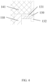
- FIG. 4 is a schematic diagram illustrating a localized structure of an exemplary cavity cover with an upper insulation member according to some embodiments of the present disclosure.
- silicon may move upwardly from the bottom portion of the growth cavity 110 or even evaporate to a gaseous state and continue to overflow upwardly as silicon vapors. Silicon vapors may spill out of the cavity cover 130 and then condense upon cooling, adhering to the surface of the upper insulation member 141, affecting its insulation properties. Accordingly, in some embodiments, as shown in FIG.
- a gap 131 may exist between the cavity cover 130 and the upper insulation member 141, and the gap 131 may be filled with carbon powder to allow the volatile silicon vapor to react with the carbon powder, so that the silicon vapor may be avoided from overflowing and condensing upon cooling and adhering to the surface of the upper insulation member 141, or the silicon carbide particles generated by the reaction of the silicon vapor with the growth cavity 110 may be avoided from adhering to the insulation assembly to affect the insulation performance.
- the cavity cover 130 may further include a raised structure 132. Due to the lower temperature (lower than the melt temperature) near the raised structure 132, some of the silicon vapors may condense at the raised structure 132 to slow down or reduce the spillover of silicon vapor and reduce the contamination degree of the upper insulation member 141. After the crystal growth is finished, the raised structure 132 may be cleaned and processed to facilitate subsequent usage.
- FIG. 5 is a schematic diagram illustrating an exemplary growth cavity according to some embodiments of the present disclosure.
- the raw material needs to be melted into a melt (liquid state) and the crystal is grown based on the melt, and the growth cavity 110 needs to be provided with a carbon source for the crystal growth.
- the bottom portion (or a lower middle portion) of the growth cavity 110 is warmer and more rapidly depleted.
- the thickness of the sidewall of the growth cavity 110 gradually increases along the direction from the top portion to the bottom portion of the growth cavity 110 (in the direction indicated by the arrows in FIG. 5 ), which accordingly prevents the bottom portion from being thinned by excessive consumption, and further allows for an increase in the number of times the growth cavity 110 may be used.
- FIG. 6 is a schematic diagram illustrating an exemplary seed crystal holder and a seed crystal according to some embodiments of the present disclosure.
- the seed crystal preparation process if the seed crystal is too thin, a burn-through phenomenon is likely to occur, which affects the effect of the crystal preparation.
- the seed crystal holder may unavoidably come into contact with the melt, generating crystals having different crystal types and/or crystallographic orientations from that of the seed crystal, thus generating crystal defects.
- the cost of the seed crystal preparation will be greatly increased.
- the one or more seed crystal may be arranged in at least two layers.
- a seed crystal used for crystal growth i.e., the lowermost layer of seed crystals in direct contact with the melt
- the other layers of seed crystals may be of a relatively lower quality, which accordingly allows for a reduction in cost while increasing the overall thickness of the seed crystal.
- the at least two layers of seed crystals may include a first seed crystal 181 and a second seed crystal 182, as illustrated in FIG. 6 .
- the mass of the first seed crystal 181 may be lower than the mass of the second seed crystal 182.
- the thickness of the first seed crystal 181 may be greater than the thickness of the second seed crystal 182 to further reduce the cost of the seed crystal 180.
- the unavoidable presence of a certain gap in the seed crystal holder 150 may lead to the escape of gas-phase material accumulated in the gap or porous regions of the backside of the seed crystal (e.g., the bonding surface of the first seed crystal 181 to the seed crystal holder 150), which may lead to defects (e.g., planar hexagonal hollow defects) in the final prepared crystal.
- defects e.g., planar hexagonal hollow defects
- a graphite paper 190 may be filled between the seed crystal holder 150 and the seed crystal 180 (the first seed crystal 181).
- the graphite paper 190 is softer and flatter, which reduces the porosity of the bonding surface, prevents uneven heating of the backside of the seed crystals, reduces subsequent defects, and improves the strength of the bond between the seed crystal holder 150 and the seed crystal 180 (e.g., the first seed crystal 181).
- FIG. 7 is a flowchart illustrating an exemplary crystal preparation process according to some embodiments of the present disclosure.
- process 700 may be performed by one or more components of a crystal preparation apparatus (e.g., the crystal preparation apparatus 100).
- the process 700 may be automatically executed by a control system.
- the process 700 may be realized by control instructions, and the control system, based on the control instructions, controls various components to perform various operations of the process 700.
- the process 700 may be executed semi-automatically.
- one or more operations of the process 700 may be manually performed by an operator.
- one or more additional operations not described may be added, and/or one or more operations discussed herein may be deleted.
- the order of the operations shown in FIG. 7 is not limiting. As shown in FIG. 7 , the process 700 includes the following operations.
- a raw material is placed inside a growth cavity.
- the raw material refers to a raw material needed to grow crystals.
- the raw material may include silicon (e.g., silicon powder, silicon wafer, silicon block).
- the raw material may include silicon and carbon (e.g., carbon powder, carbon block, carbon particle).
- the raw material includes carbon powder, carbon block, or carbon particle, which may increase the number of times the growth cavity is used.
- the raw material may also include a flux to increase the solubility of carbon in silicon.
- the flux may include, but is not limited to, aluminum, silicon-chromium alloys, Li-Si alloys, Ti-Si alloys, Fe-Si alloys, Sc-Si alloys, Co-Si alloys.
- each of one or more plate assemblies may be arranged in a layer within the growth cavity.
- the growth cavity e.g., the growth cavity 110
- the at least one layer of plate assemblies e.g., the plate assemblies 111
- the growth cavity is heated by a heating assembly to melt the raw material into a melt.
- the raw material when growing silicon carbide crystal, the raw material is melted to form a solution of carbon in silicon, which serves as a liquid raw material for crystal growth.
- heating assembly e.g., the heating assembly 120
- FIG. 1 Related descriptions of the heating assembly may be found elsewhere in the present disclosure (e.g., FIG. 1 and its description) and will not be repeated here.
- a ratio of the height of the melt to the height of the growth cavity needs to be within a predetermined range in order to improve the utilization of the raw material.
- the ratio of the height of the melt to the height of the growth cavity may be within a range of 1:1-1:5. In some embodiments, the ratio of the height of the melt to the height of the growth cavity may be within a range of 1:1.5-1:4.5. In some embodiments, the ratio of the height of the melt to the height of the growth cavity may be within a range of 1 :2-1:4. In some embodiments, the ratio of the height of the melt to the height of the growth cavity may be within a range of 1 :2.5-1 :3.5. In some embodiments, the ratio of the height of the melt to the height of the growth cavity may be within a range of 1:2.8-1:3.
- the melt level may be located near the midpoint of the height of the heating assembly (e.g., an induction coil) to improve the stability of the crystal growth.
- "near" refers to within a predetermined distance.
- the predetermined distance may include ⁇ 50 cm, ⁇ 40 cm, ⁇ 30 cm, ⁇ 20 cm, ⁇ 10 cm, ⁇ 8 cm, ⁇ 6 cm, ⁇ 4 cm, ⁇ 2 cm, ⁇ 1 cm etc.
- the melt level may be located within ⁇ 30 cm of 1/2 the height of the heating assembly (e.g., an induction coil).
- one or more seed crystals are bonded to a seed crystal holder.
- the seed crystals may be arranged in at least two layers.
- the at least two layers of seed crystals may include a first seed crystal and a second seed crystal.
- the first seed crystal may be bonded to the seed crystal holder, and the second seed crystal may be bonded to the first seed crystal.
- the mass of the first seed crystal may be lower than the mass of the second seed crystal.
- a graphite paper may be bonded to the seed crystal holder such that the graphite paper is disposed between the seed crystal holder and a seed crystal.
- the seed crystals and/or the graphite paper may be concentric with the seed crystal holder.
- the thickness of the graphite paper may be within a range of 0.5 mm-1 mm. In some embodiments, the thickness of the graphite paper may be within a range of 0.6 mm-0.9 mm. In some embodiments, the thickness of the graphite paper may be within a range of 0.5 mm-1 mm. In some embodiments, the thickness of the graphite paper may be within a range of 0.7 mm-0.8 mm.
- the flatness of the surface of the first seed crystal is required to satisfy a predetermined condition.
- the flatness of the surface of the first seed crystal adhered to the graphite paper may be less than 0.01 mm.
- the flatness of the surface of the first seed crystal adhered to the second seed crystal may be within a range of 0.005 mm-0.008 mm.
- the flatness of the surface of the first seed crystal affixed to the second seed crystal may be within a range of 0.006 mm-0.007 mm.
- seed crystals e.g., the seed crystal 180
- seed crystal holder e.g., the seed crystal holder 150
- the seed crystal holder with the seed crystals is lowered so that the seed crystals are in contact with the melt.
- the connecting assembly may be driven down by the power assembly to drive the seed crystal holder down to bring the seed crystals into contact with the melt.
- a crystal is prepared based on the seed crystals and the melt.
- the connecting assembly may be driven by the power assembly to rotate and/or move up and down to drive the seed crystal holder to rotate and/or move up and down, and the melt may be condensed and crystallized at the seed crystals to grow the crystal.
- one or more plate assemblies each of which is arranged in a layer are provided inside the growth cavity, and the material of the plate assemblies includes graphite, which may be used as a carbon source to provide the raw material required for the preparation of the silicon carbide crystals.
- the plate assemblies include through holes, and the through holes on the adjacent plate assemblies are staggered, which may regulate the convection of the melt inside the growth cavity, reduce the volatile components (e.g., silicon), reduce the volatility of volatile components (e.g., silicon) on the surface of the melt, reduce the excessive consumption of volatile components, and reduce the silicon carbide particles generated by the reaction of volatile components (e.g., silicon vapor) with the growth cavity, which further reduces the contamination degree of the insulation member, ensures the insulation performance of the insulation member, and further ensures the normal growth of the crystal.
- the volatile components e.g., silicon
- reduce the volatility of volatile components (e.g., silicon) on the surface of the melt reduce the excessive consumption of volatile components
- reduce the silicon carbide particles generated by the reaction of volatile components (e.g., silicon vapor) with the growth cavity which further reduces the contamination degree of the insulation member, ensures the insulation performance of the insulation member, and further ensures the normal growth of the crystal.
- the upper portion with the predetermined range of the sidewall of the growth cavity is coated with a coating or provided with a shielding ring, which avoids the reaction between the silicon on the surface of the melt and the carbon on the sidewall of the growth cavity, thereby avoiding spontaneous nucleation of crystalline growth.
- the carbon powder may react with the volatile silicon vapor to prevent silicon vapor from overflowing to the insulation member, or to prevent the silicon carbide particles generated by the reaction between the silicon vapor and the growth cavity from attaching to the insulation member and affecting its insulation performance.
- the cavity cover includes a raised structure, which allows part of the silicon vapor to condense at the raised structure to slow down or reduce the overflow of silicon vapor and reduce the contamination degree of the insulation member.
- the seed crystals include one or more seed crystals arrange in at least two layers, which may increase the thickness of the seed crystals, reduce the risk of the seed crystals being burned through, and further ensure the quality of the produced crystals.
- the mass of the first seed crystal bonded to the seed crystal holder may be lower than the mass of the second seed crystal bonded to the first seed crystal, which reduces the cost of the seed crystals and further reduce the cost of the crystal preparation.
- beneficial effects that may be produced by different embodiments are different, and the beneficial effects that may be produced in different embodiments may be any one or a combination of any one or a combination of any of the foregoing, or any other beneficial effect that may be obtained.
- the numbers expressing quantities or properties used to describe and claim certain embodiments of the present disclosure are to be understood as being modified in some instances by the term “about”, “approximate”, or “substantially”. For example, “about”, “approximate”, or “substantially” may indicate ⁇ 20% variation of the value it describes, unless otherwise stated. Accordingly, in some embodiments, the numerical parameters set forth in the written description and attached claims are approximations that may vary depending upon the desired properties sought to be obtained by a particular embodiment. In some embodiments, the numerical parameters should be construed in light of the number of reported significant digits and by applying ordinary rounding techniques. Notwithstanding that the numerical ranges and parameters setting forth the broad scope of some embodiments of the present disclosure are approximations, the numerical values set forth in the specific examples are reported as precisely as practicable.
Landscapes
- Chemical & Material Sciences (AREA)
- Engineering & Computer Science (AREA)
- Crystallography & Structural Chemistry (AREA)
- Materials Engineering (AREA)
- Metallurgy (AREA)
- Organic Chemistry (AREA)
- Inorganic Chemistry (AREA)
- Crystals, And After-Treatments Of Crystals (AREA)
Applications Claiming Priority (1)
| Application Number | Priority Date | Filing Date | Title |
|---|---|---|---|
| PCT/CN2022/097279 WO2023236025A1 (zh) | 2022-06-07 | 2022-06-07 | 一种晶体制备装置及晶体制备方法 |
Publications (2)
| Publication Number | Publication Date |
|---|---|
| EP4512940A1 true EP4512940A1 (de) | 2025-02-26 |
| EP4512940A4 EP4512940A4 (de) | 2025-04-23 |
Family
ID=89117301
Family Applications (1)
| Application Number | Title | Priority Date | Filing Date |
|---|---|---|---|
| EP22945175.2A Pending EP4512940A4 (de) | 2022-06-07 | 2022-06-07 | Kristallherstellungsvorrichtung und kristallherstellungsverfahren |
Country Status (6)
| Country | Link |
|---|---|
| US (1) | US20250084558A1 (de) |
| EP (1) | EP4512940A4 (de) |
| JP (1) | JP2025518023A (de) |
| KR (1) | KR20250013228A (de) |
| CN (1) | CN119137317A (de) |
| WO (1) | WO2023236025A1 (de) |
Family Cites Families (12)
| Publication number | Priority date | Publication date | Assignee | Title |
|---|---|---|---|---|
| US6336971B1 (en) * | 1997-09-12 | 2002-01-08 | Showa Denko Kabushiki Kaisha | Method and apparatus for producing silicon carbide single crystal |
| JP5936344B2 (ja) * | 2011-12-16 | 2016-06-22 | 株式会社豊田自動織機 | SiC結晶の成長方法およびSiC結晶の製造装置 |
| JP2015140291A (ja) * | 2014-01-29 | 2015-08-03 | 住友金属鉱山株式会社 | サファイア単結晶育成用坩堝およびこの坩堝を用いたサファイア単結晶の製造方法 |
| KR102049021B1 (ko) * | 2016-03-09 | 2019-11-26 | 주식회사 엘지화학 | 실리콘 카바이드 단결정 성장 장치 |
| CN206624942U (zh) * | 2016-12-19 | 2017-11-10 | 山东天岳先进材料科技有限公司 | 一种物理气相输运法生长碳化硅晶体的装置 |
| KR102107626B1 (ko) * | 2018-07-20 | 2020-05-08 | 재단법인 포항산업과학연구원 | 탄화규소 단결정 성장 장치 및 탄화규소 단결정 성장 방법 |
| CN109629001A (zh) * | 2019-02-02 | 2019-04-16 | 福建北电新材料科技有限公司 | 碳化硅单晶生长装置及碳化硅单晶制备设备 |
| CN111621851B (zh) * | 2020-04-22 | 2021-03-30 | 浙江博蓝特半导体科技股份有限公司 | 碳化硅晶体的生长装置及生长方法 |
| CN111254486A (zh) * | 2020-05-06 | 2020-06-09 | 眉山博雅新材料有限公司 | 一种晶体制备装置 |
| CN111424318B (zh) * | 2020-06-10 | 2020-10-16 | 眉山博雅新材料有限公司 | 一种用于制备掺杂yag单晶光纤的方法 |
| CN113308737B (zh) * | 2021-05-25 | 2022-04-19 | 眉山博雅新材料股份有限公司 | 一种yag单晶包层制备方法及装置 |
| CN216039934U (zh) * | 2021-11-08 | 2022-03-15 | 福建北电新材料科技有限公司 | 一种碳化硅晶体生长装置和设备 |
-
2022
- 2022-06-07 CN CN202280095309.6A patent/CN119137317A/zh active Pending
- 2022-06-07 JP JP2024569388A patent/JP2025518023A/ja active Pending
- 2022-06-07 EP EP22945175.2A patent/EP4512940A4/de active Pending
- 2022-06-07 KR KR1020247042691A patent/KR20250013228A/ko active Pending
- 2022-06-07 WO PCT/CN2022/097279 patent/WO2023236025A1/zh not_active Ceased
-
2024
- 2024-11-26 US US18/959,743 patent/US20250084558A1/en active Pending
Also Published As
| Publication number | Publication date |
|---|---|
| JP2025518023A (ja) | 2025-06-12 |
| CN119137317A (zh) | 2024-12-13 |
| WO2023236025A1 (zh) | 2023-12-14 |
| KR20250013228A (ko) | 2025-01-31 |
| US20250084558A1 (en) | 2025-03-13 |
| EP4512940A4 (de) | 2025-04-23 |
Similar Documents
| Publication | Publication Date | Title |
|---|---|---|
| CN104471117B (zh) | SiC单晶体的制造装置和SiC单晶体的制造方法 | |
| JP7025395B2 (ja) | 単結晶成長炉の反射スクリーン及び単結晶成長炉 | |
| US20130269598A1 (en) | Process for growing silicon carbide single crystal by physical vapor transport method and annealing silicon carbide single crystal in situ | |
| EP3619339B1 (de) | Kristallzüchtungssystem und -verfahren mit tiegel und barriere | |
| CN111088524B (zh) | 一种大尺寸碳化硅单晶、衬底及制备方法和使用的装置 | |
| DE102010029756A1 (de) | Herstellungsverfahren für einen SiC-Volumeneinkristall mit großer Facette und einkristallines SiC-Substrat mit homogener Widerstandsverteilung | |
| KR20100048836A (ko) | 다층 구조를 갖는 석영 유리 도가니 | |
| WO2009139447A1 (ja) | 単結晶の製造装置及び製造方法 | |
| CN102317511A (zh) | 硅单结晶拉升用石英玻璃坩埚及硅单结晶的制造方法 | |
| CN103930601B (zh) | SiC单晶的制造方法 | |
| EP4512940A1 (de) | Kristallherstellungsvorrichtung und kristallherstellungsverfahren | |
| CN110453285A (zh) | 坩埚盖及坩埚 | |
| US20260043168A1 (en) | Enclosed crystal growth | |
| JP6326136B2 (ja) | 単結晶成長装置 | |
| DE102010023101A1 (de) | Verfahren zur Herstellung von Halbleiterscheiben aus Silizium | |
| WO2012026062A1 (ja) | 半導体単結晶の製造装置及び製造方法 | |
| TW202400856A (zh) | 晶體製備裝置及晶體製備方法 | |
| JP5425858B2 (ja) | 再使用が可能なシリコン溶融用二重坩堝を備える単結晶シリコンインゴット成長装置 | |
| CN114875476B (zh) | 一种晶体制备装置 | |
| US20140190402A1 (en) | Apparatus and method for manufacturing ingot | |
| CN218089894U (zh) | 一种碳化硅单晶生长装置 | |
| CN121046957B (zh) | 碳化硅单晶生长装置及其工作方法 | |
| JP2012201568A (ja) | 炭化ケイ素単結晶の製造装置及び炭化ケイ素単結晶基板 | |
| JP2011051824A (ja) | 単結晶製造装置 | |
| JP6061977B2 (ja) | シリコンの単結晶を製造するための装置およびプロセス |
Legal Events
| Date | Code | Title | Description |
|---|---|---|---|
| STAA | Information on the status of an ep patent application or granted ep patent |
Free format text: STATUS: THE INTERNATIONAL PUBLICATION HAS BEEN MADE |
|
| PUAI | Public reference made under article 153(3) epc to a published international application that has entered the european phase |
Free format text: ORIGINAL CODE: 0009012 |
|
| STAA | Information on the status of an ep patent application or granted ep patent |
Free format text: STATUS: REQUEST FOR EXAMINATION WAS MADE |
|
| 17P | Request for examination filed |
Effective date: 20241119 |
|
| AK | Designated contracting states |
Kind code of ref document: A1 Designated state(s): AL AT BE BG CH CY CZ DE DK EE ES FI FR GB GR HR HU IE IS IT LI LT LU LV MC MK MT NL NO PL PT RO RS SE SI SK SM TR |
|
| REG | Reference to a national code |
Ref country code: DE Ref legal event code: R079 Free format text: PREVIOUS MAIN CLASS: C30B0015000000 Ipc: C30B0029360000 |
|
| A4 | Supplementary search report drawn up and despatched |
Effective date: 20250326 |
|
| RIC1 | Information provided on ipc code assigned before grant |
Ipc: C30B 19/04 20060101ALI20250320BHEP Ipc: C30B 19/06 20060101ALI20250320BHEP Ipc: C30B 29/36 20060101AFI20250320BHEP |
|
| DAV | Request for validation of the european patent (deleted) | ||
| DAX | Request for extension of the european patent (deleted) |