EP4503872A1 - Circuit board - Google Patents
Circuit board Download PDFInfo
- Publication number
- EP4503872A1 EP4503872A1 EP23780830.8A EP23780830A EP4503872A1 EP 4503872 A1 EP4503872 A1 EP 4503872A1 EP 23780830 A EP23780830 A EP 23780830A EP 4503872 A1 EP4503872 A1 EP 4503872A1
- Authority
- EP
- European Patent Office
- Prior art keywords
- hole
- electrical conductor
- hole electrical
- filling resin
- insulating layer
- Prior art date
- Legal status (The legal status is an assumption and is not a legal conclusion. Google has not performed a legal analysis and makes no representation as to the accuracy of the status listed.)
- Withdrawn
Links
Images


Classifications
-
- H—ELECTRICITY
- H05—ELECTRIC TECHNIQUES NOT OTHERWISE PROVIDED FOR
- H05K—PRINTED CIRCUITS; CASINGS OR CONSTRUCTIONAL DETAILS OF ELECTRIC APPARATUS; MANUFACTURE OF ASSEMBLAGES OF ELECTRICAL COMPONENTS
- H05K1/00—Printed circuits
- H05K1/02—Details
- H05K1/0271—Arrangements for reducing stress or warp in rigid printed circuit boards, e.g. caused by loads, vibrations or differences in thermal expansion
-
- H—ELECTRICITY
- H05—ELECTRIC TECHNIQUES NOT OTHERWISE PROVIDED FOR
- H05K—PRINTED CIRCUITS; CASINGS OR CONSTRUCTIONAL DETAILS OF ELECTRIC APPARATUS; MANUFACTURE OF ASSEMBLAGES OF ELECTRICAL COMPONENTS
- H05K1/00—Printed circuits
- H05K1/02—Details
- H05K1/11—Printed elements for providing electric connections to or between printed circuits
- H05K1/115—Via connections; Lands around holes or via connections
-
- H—ELECTRICITY
- H05—ELECTRIC TECHNIQUES NOT OTHERWISE PROVIDED FOR
- H05K—PRINTED CIRCUITS; CASINGS OR CONSTRUCTIONAL DETAILS OF ELECTRIC APPARATUS; MANUFACTURE OF ASSEMBLAGES OF ELECTRICAL COMPONENTS
- H05K1/00—Printed circuits
- H05K1/02—Details
- H05K1/11—Printed elements for providing electric connections to or between printed circuits
- H05K1/115—Via connections; Lands around holes or via connections
- H05K1/116—Lands, clearance holes or other lay-out details concerning the surrounding of a via
-
- H—ELECTRICITY
- H05—ELECTRIC TECHNIQUES NOT OTHERWISE PROVIDED FOR
- H05K—PRINTED CIRCUITS; CASINGS OR CONSTRUCTIONAL DETAILS OF ELECTRIC APPARATUS; MANUFACTURE OF ASSEMBLAGES OF ELECTRICAL COMPONENTS
- H05K3/00—Apparatus or processes for manufacturing printed circuits
- H05K3/0094—Filling or covering plated through-holes or blind plated vias, e.g. for masking or for mechanical reinforcement
-
- H—ELECTRICITY
- H05—ELECTRIC TECHNIQUES NOT OTHERWISE PROVIDED FOR
- H05K—PRINTED CIRCUITS; CASINGS OR CONSTRUCTIONAL DETAILS OF ELECTRIC APPARATUS; MANUFACTURE OF ASSEMBLAGES OF ELECTRICAL COMPONENTS
- H05K3/00—Apparatus or processes for manufacturing printed circuits
- H05K3/40—Forming printed elements for providing electric connections to or between printed circuits
- H05K3/42—Plated through-holes or plated via connections
- H05K3/425—Plated through-holes or plated via connections characterised by the sequence of steps for plating the through-holes or via connections in relation to the conductive pattern
- H05K3/427—Plated through-holes or plated via connections characterised by the sequence of steps for plating the through-holes or via connections in relation to the conductive pattern initial plating of through-holes in metal-clad substrates
-
- H—ELECTRICITY
- H05—ELECTRIC TECHNIQUES NOT OTHERWISE PROVIDED FOR
- H05K—PRINTED CIRCUITS; CASINGS OR CONSTRUCTIONAL DETAILS OF ELECTRIC APPARATUS; MANUFACTURE OF ASSEMBLAGES OF ELECTRICAL COMPONENTS
- H05K3/00—Apparatus or processes for manufacturing printed circuits
- H05K3/46—Manufacturing multilayer circuits
- H05K3/4602—Manufacturing multilayer circuits characterized by a special circuit board as base or central core whereon additional circuit layers are built or additional circuit boards are laminated
-
- H—ELECTRICITY
- H05—ELECTRIC TECHNIQUES NOT OTHERWISE PROVIDED FOR
- H05K—PRINTED CIRCUITS; CASINGS OR CONSTRUCTIONAL DETAILS OF ELECTRIC APPARATUS; MANUFACTURE OF ASSEMBLAGES OF ELECTRICAL COMPONENTS
- H05K3/00—Apparatus or processes for manufacturing printed circuits
- H05K3/46—Manufacturing multilayer circuits
- H05K3/4644—Manufacturing multilayer circuits by building the multilayer layer by layer, i.e. build-up multilayer circuits
- H05K3/4673—Application methods or materials of intermediate insulating layers not specially adapted to any one of the previous methods of adding a circuit layer
-
- H—ELECTRICITY
- H05—ELECTRIC TECHNIQUES NOT OTHERWISE PROVIDED FOR
- H05K—PRINTED CIRCUITS; CASINGS OR CONSTRUCTIONAL DETAILS OF ELECTRIC APPARATUS; MANUFACTURE OF ASSEMBLAGES OF ELECTRICAL COMPONENTS
- H05K3/00—Apparatus or processes for manufacturing printed circuits
- H05K3/46—Manufacturing multilayer circuits
- H05K3/4688—Composite multilayer circuits, i.e. comprising insulating layers having different properties
-
- H—ELECTRICITY
- H05—ELECTRIC TECHNIQUES NOT OTHERWISE PROVIDED FOR
- H05K—PRINTED CIRCUITS; CASINGS OR CONSTRUCTIONAL DETAILS OF ELECTRIC APPARATUS; MANUFACTURE OF ASSEMBLAGES OF ELECTRICAL COMPONENTS
- H05K2201/00—Indexing scheme relating to printed circuits covered by H05K1/00
- H05K2201/09—Shape and layout
- H05K2201/09209—Shape and layout details of conductors
- H05K2201/09372—Pads and lands
- H05K2201/09481—Via in pad; Pad over filled via
-
- H—ELECTRICITY
- H05—ELECTRIC TECHNIQUES NOT OTHERWISE PROVIDED FOR
- H05K—PRINTED CIRCUITS; CASINGS OR CONSTRUCTIONAL DETAILS OF ELECTRIC APPARATUS; MANUFACTURE OF ASSEMBLAGES OF ELECTRICAL COMPONENTS
- H05K2201/00—Indexing scheme relating to printed circuits covered by H05K1/00
- H05K2201/09—Shape and layout
- H05K2201/09209—Shape and layout details of conductors
- H05K2201/095—Conductive through-holes or vias
- H05K2201/0959—Plated through-holes or plated blind vias filled with insulating material
-
- H—ELECTRICITY
- H05—ELECTRIC TECHNIQUES NOT OTHERWISE PROVIDED FOR
- H05K—PRINTED CIRCUITS; CASINGS OR CONSTRUCTIONAL DETAILS OF ELECTRIC APPARATUS; MANUFACTURE OF ASSEMBLAGES OF ELECTRICAL COMPONENTS
- H05K2201/00—Indexing scheme relating to printed circuits covered by H05K1/00
- H05K2201/09—Shape and layout
- H05K2201/09209—Shape and layout details of conductors
- H05K2201/095—Conductive through-holes or vias
- H05K2201/096—Vertically aligned vias, holes or stacked vias
-
- H—ELECTRICITY
- H05—ELECTRIC TECHNIQUES NOT OTHERWISE PROVIDED FOR
- H05K—PRINTED CIRCUITS; CASINGS OR CONSTRUCTIONAL DETAILS OF ELECTRIC APPARATUS; MANUFACTURE OF ASSEMBLAGES OF ELECTRICAL COMPONENTS
- H05K2201/00—Indexing scheme relating to printed circuits covered by H05K1/00
- H05K2201/09—Shape and layout
- H05K2201/09209—Shape and layout details of conductors
- H05K2201/095—Conductive through-holes or vias
- H05K2201/09618—Via fence, i.e. one-dimensional array of vias
-
- H—ELECTRICITY
- H05—ELECTRIC TECHNIQUES NOT OTHERWISE PROVIDED FOR
- H05K—PRINTED CIRCUITS; CASINGS OR CONSTRUCTIONAL DETAILS OF ELECTRIC APPARATUS; MANUFACTURE OF ASSEMBLAGES OF ELECTRICAL COMPONENTS
- H05K2201/00—Indexing scheme relating to printed circuits covered by H05K1/00
- H05K2201/09—Shape and layout
- H05K2201/09818—Shape or layout details not covered by a single group of H05K2201/09009 - H05K2201/09809
- H05K2201/09827—Tapered, e.g. tapered hole, via or groove
Definitions
- the present invention relates to a wiring board.
- a through-hole electrical conductor is filled in a through hole and there is a case where a through-hole electrical conductor is formed only on an inner wall surface of a through hole and a remaining portion in the through hole is filled with a resin.
- a wiring board described in Patent Document 1 an electrical conductor film is located on an inner wall surface of a through hole, and a filler formed of resin is located in a remaining portion in the through hole.
- Patent Document 1 JP 2021-27167 A
- a wiring board includes an insulating layer including a first surface and a second surface opposite the first surface, a through hole having openings in the first surface and the second surface of the insulating layer, a through-hole electrical conductor located from a periphery of the opening in the first surface to a periphery of the opening in the second surface via an inner wall surface of the through hole, and a filling resin located in a region surrounded by the through-hole electrical conductor and including two surfaces that are a first surface on the first surface side and a second surface on the second surface side.
- the through-hole electrical conductor includes a first through-hole electrical conductor.
- the first through-hole electrical conductor includes a protruding portion extending to an inside of the through hole in at least one opening of the through hole.
- an angle formed between a portion of the protruding portion adjacent to the filling resin and at least the first surface or the second surface of the filling resin is an obtuse angle.
- a wiring board according to an embodiment of the present disclosure has a configuration as described in the section of Summary of the Invention, so that cracks occurring in the through-hole electrical conductor are reduced and excellent electrical reliability is ensured.
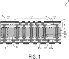
- FIG. 1 is a cross-sectional view illustrating a wiring board 1 according to an embodiment of the present disclosure.
- the wiring board 1 according to a first embodiment includes a core insulating layer 2, a build-up layer 3, and a solder resist 6.
- the core insulating layer 2 is not particularly limited as long as it is formed of a material having an insulating property.
- the material having the insulating property include resins such as an epoxy resin, a bismaleimide-triazine resin, a polyimide resin, and a polyphenylene ether resin. Two or more types of these resins may be mixed and used.
- the thickness of the core insulating layer 2 is not particularly limited and is, for example, 800 ⁇ m or greater and 1400 ⁇ m or less.
- the core insulating layer 2 may include a reinforcing material.
- the reinforcing material include insulating fabric materials such as glass fiber, glass non-woven fabric, aramid non-woven fabric, aramid fiber, and polyester fiber. Two or more types of reinforcing materials may be used in combination.
- An inorganic insulating filler such as silica, barium sulfate, talc, clay, glass, calcium carbonate, or titanium oxide may be dispersed in the core insulating layer 2. Two or more types of inorganic insulating fillers may be used in combination.
- the build-up layer 3 is located on each of a first surface and a second surface of the core insulating layer 2.
- the first surface and the second surface refer to an upper surface and a lower surface. In FIG. 1 , for convenience, the first surface is referred to as an upper surface and the second surface is referred to as a lower surface.
- the build-up layer 3 has a structure in which an electrical conductor layer 4 and a build-up insulating layer 5 are alternately layered.
- the electrical conductor layer 4 included in the build-up layer 3 is formed of an electrical conductor such as copper foil or copper plating, for example.
- the thickness of the electrical conductor layer 4 is not particularly limited and is, for example, 15 ⁇ m or greater and 30 ⁇ m or less.
- the build-up insulating layer 5 included in the build-up layer 3 is not particularly limited as long as the build-up insulating layer is formed of a material having an insulating property.
- the material having an insulating property include resins such as an epoxy resin, a bismaleimide-triazine resin, a polyimide resin, and a polyphenylene ether resin. Two or more types of these resins may be mixed and used.
- the respective build-up insulating layers 5 may be formed of the same resin or may be formed of different resins.
- the build-up insulating layer 5 included in the build-up layer 3 and the core insulating layer 2 may be formed of the same resin or may be formed of different resins.
- the build-up insulating layer 5 included in the build-up layer 3 may include a reinforcing material, as with the core insulating layer 2.
- the reinforcing material include insulating fabric materials such as glass fiber, glass non-woven fabric, aramid non-woven fabric, aramid fiber, and polyester fiber. Two or more types of reinforcing materials may be used in combination.
- an inorganic insulating filler such as silica, barium sulfate, talc, clay, glass, calcium carbonate, or titanium oxide may be dispersed in the build-up insulating layer 5. Two or more types of inorganic insulating fillers may be used in combination.
- the thickness of the build-up insulating layer 5 included in the build-up layer 3 is not particularly limited and is, for example, 25 ⁇ m or greater and 60 ⁇ m or less. When two or more build-up insulating layers 5 are present in the build-up layer 3, the respective build-up insulating layers 5 may have the same thickness or may have different thicknesses.
- a via hole electrical conductor for electrically connecting layers is included in the build-up insulating layer 5 included in the build-up layer 3.
- the via hole electrical conductor is located in a via hole penetrating through upper and lower surfaces of the build-up insulating layer 5 included in the build-up layer 3.
- the via hole electrical conductor is formed of an electrical conductor such as metal plating, for example, copper plating.
- the via hole electrical conductor is connected to the electrical conductor layers 4 located on the upper and lower surfaces of the build-up insulating layer 5 included in the build-up layer 3.
- the via hole electrical conductor may be filled in the via hole, or may be located only on an inner wall surface of the via hole.
- Solder resists 6 are located on a part of both surfaces of the wiring board 1 according to the first embodiment.
- the solder resist 6 is formed of, for example, an acryl-modified epoxy resin.
- the solder resist 6 has a function of protecting the electrical conductor layer 4 from solder adhesion when, for example, mounting an electronic component.
- the core insulating layer 2 includes a first through-hole electrical conductor 21 and a second through-hole electrical conductor 22 so as to electrically connect the first and second surfaces (upper and lower surfaces) of the core insulating layer 2.
- the first through-hole electrical conductor 21 and the second through-hole electrical conductor 22 are located in through holes 2a and 2b penetrating through the upper and lower surfaces of the core insulating layer 2.
- the first through-hole electrical conductor 21 and the second through-hole electrical conductor 22 have, for example, tubular shapes in the through holes 2a and 2b, are formed of electrical conductors such as metal (for example, copper), and are connected to the electrical conductor layers 4 located on the upper and lower surfaces of the core insulating layer 2.
- the first through-hole electrical conductor 21 located in the through hole 2a is located in a first region 11, for example, as illustrated in FIG. 1 .
- the first region 11 is a region having a first occupancy rate in which a ratio of an opening area of the through hole 2a to a unit area is relatively high.
- the first occupancy rate can be calculated, for example, by reading the number of through holes 2a located in 1 mm 2 from an enlarged photograph of a surface of the core insulating layer 2 and multiplying the number by an opening area (mm 2 ) per through hole 2a.
- the opening area of the through hole 2a is, for example, 0.07 mm 2 or greater per surface 1 mm 2 of the core insulating layer 2.
- the first through-hole electrical conductor 21 is located from a periphery of the opening in the first surface of the core insulating layer 2 to a periphery of the opening in the second surface via the inner wall surface of the through hole 2a.
- the first through-hole electrical conductor 21 has a protruding portion 211 extending to an inside of the through hole 2a in at least one opening of the through hole 2a.
- the protruding portions 211 are provided in both openings of the through hole 2a.
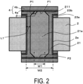
- FIG. 2 is an enlarged illustration view for illustrating a region X illustrated in FIG. 1 .
- the first through-hole electrical conductor 21 is not filled in the through hole 2a.
- a filling resin 21a fills a portion other than the first through-hole electrical conductor 21.
- the filling resin 21a has a pillar shape in which a surface (end surface) located at the uppermost portion on the first surface side of the core insulating layer 2 is a first surface F1 and a surface (end surface) located at the lowermost portion on the second surface side is a second surface F2.
- the filling resin 21a include resins such as an epoxy resin, a bismaleimide-triazine resin, a polyimide resin, and a polyphenylene ether resin.
- the width of at least one of the first surface F 1 and the second surface F2 of the filling resin 21a may be 40% or greater and 90% or less of a width of the through hole 2a.
- the width of at least one of the first surface F1 and the second surface F2 of the filling resin 21a is denoted as W1 and the width of the through hole 2a is denoted as W2
- the length of the width W1 may be 40% or greater and 90% or less of the length of the width W2.
- the width of at least one of the first surface F 1 and the second surface F2 of the filling resin 21a is within such a range, it is possible to ensure the thickness of the first through-hole electrical conductor 21 in the vicinity of the opening of the through hole 2a and improve the strength, while maintaining the ease of filling of the filling resin 21a.
- an angle ⁇ formed between a portion P1 of the protruding portion 211 adjacent to the filling resin 21a and the first surface F1 of the filling resin 21a is an obtuse angle.
- the angle ⁇ is not limited as long as it is an obtuse angle, and may be, for example, 100° or greater and 160° or less.
- the angles ⁇ may be different from each other as long as they are obtuse angles.
- the "cross section" in the cross-sectional view refers to a cross section in a depth direction of the through hole 2a (a thickness direction of the core insulating layer 2).
- the through-hole land is a land electrical conductor that is part of the electrical conductor layer 4, and is located on the surface of the filling resin 21a located on the first surface side (the first surface F1 of the filling resin 21a), the surface of the filling resin 21a located on the second surface side (the second surfaces F2 of the filling resin 21a), and the surface of the through-hole electrical conductor (the first through-hole electrical conductor 21) located on the first and second surfaces of the core insulating layer 2.
- the second through-hole electrical conductor 22 is located in the through hole 2b of the core insulating layer 2. As illustrated in FIG. 1 , the through hole 2b is located, for example, in a second region 12.
- the second region 12 is a region in which the ratio of the opening area of the through hole 2b to the unit area has a second occupancy rate lower than the first occupancy rate. In the second region 12, the opening area of the through hole 2b is, for example, 0.05 mm 2 or less per surface 1 mm 2 of the core insulating layer 2.
- the second occupancy rate can be calculated, for example, by reading the number of the through holes 2b located in 1 mm 2 from an enlarged photograph of a surface of the core insulating layer 2 and multiplying the number by an opening area (mm 2 ) per through hole 2b.
- the second through-hole electrical conductor 22 is also located from a periphery of an opening in the first surface of the core insulating layer 2 to a periphery of an opening in the second surface via the inner wall surface of the through hole 2b. As illustrated in FIG. 3 , the second through-hole electrical conductor 22 does not have the protruding portion 211 that the first through-hole electrical conductor 21 has.
- FIG. 3 is an enlarged illustration view for illustrating a region Y illustrated in FIG. 1 .
- the second through-hole electrical conductor 22 is not filled in the through hole 2b, and the remaining portion in the through hole 2b is filled with a filling resin 22a.
- the filling resin 22a is similar to the filling resin 21a, and detailed description thereof will be omitted.
- the second through-hole electrical conductor 22 does not have the protruding portion 211. That is, widths of the surface (first surface F1) on the first surface side and the surface (second surface F2) on the second surface side of the filling resin 22a surrounded by the second through-hole electrical conductor 22 are greater than the widths of the first surface F1 and the second surface F2 of the filling resin 21a surrounded by the first through-hole electrical conductor 21 because of the absence of the protruding portions 211.
- the via electrical conductors located in the build-up insulating layer 5 are less likely to be layered. For this reason, stress is less likely to be applied to the through-hole land located in the lower layer. Therefore, the filling resin 22a has a structure excellent in filling property without providing the protruding portion 211.
- a thickness L2 of the second through-hole electrical conductor 22 located on the inner wall of the through hole 2b may be greater than a thickness L1 of the first through-hole electrical conductor 21 located on the inner wall of the through hole 2a.
- the first through-hole electrical conductor 21 located on the inner wall of the through hole 2a may have the thickness L1 of, for example, 10 ⁇ m or greater and 40 ⁇ m or less.
- the second through-hole electrical conductor 22 located on the inner wall of the through hole 2b may have the thickness L2 of, for example, 10 ⁇ m or greater and 40 ⁇ m or less. Within these ranges, the thickness L2 of the second through-hole electrical conductor 22 may be greater than the thickness L 1 of the first through-hole electrical conductor 21.
- the thickness of the electrical conductor located on the inner wall can be, for example, an average value of values obtained by measuring the thickness of the conductor at three points in a direction perpendicular to the inner wall of the through hole.
- the rigidity of the wiring board 1 can be improved by increasing the thickness of the portion of the second through-hole electrical conductor 22 located on the inner wall of the through hole 2b. As a result, bending of the wiring board 1 can be reduced. In the second region 12, the wiring tends to be longer than that in the first region 11, and the conduction resistance becomes high. By thickening the portion of the second through-hole electrical conductor 22 located on the inner wall of the through hole 2b, the conduction resistance can be reduced.
- a metal layer 23a, a seed layer 23b, a seed layer 4a, and an electrolytic plating metal layer 4b illustrated in FIGs. 2 and 3 will be described together with the process of forming a region X described below.
- a method of forming the first through-hole electrical conductor 21 in the through hole 2a and filling the filling resin 21a is not limited, and they are formed by, for example, a process as illustrated in FIGs. 4 and 5 .
- FIGs. 4 and 5 are illustration views for illustrating a process for forming the region X illustrated in FIG. 1 .
- a double-sided metal-clad laminate plate is prepared in which metal layers 23a such as copper are layered on both surfaces of a core insulating layer 2.
- the thickness of the metal layer 23a is, for example, 2 ⁇ m or greater and 20 ⁇ m or less.
- the core insulating layer 2 is as described above, and thus detailed description thereof will be omitted.
- a through hole 2a is formed in the double-sided metal-clad laminate plate.
- the method of forming the through hole 2a is not particularly limited, and the through hole is formed using, for example, a drill or the like. At this time, an opening corner portion of the through hole 2a may be formed to be substantially right-angled, as with a general through hole.
- a desmear treatment is performed to remove residues such as resin.
- an electroless plating treatment is performed on an inner wall surface of the through hole 2a and a surface of the metal layer 23a to form a seed layer 23b formed of metal such as copper.
- an electrolytic plating treatment is performed to form a first through-hole electrical conductor 21 on a surface of the seed layer 23b. Since the current density is concentrated at the opening corner portion of the through hole 2a, the first through-hole electrical conductor 21 is formed thick so as to protrude to the inside of the through hole 2a.
- a filling resin 21a is filled in the through hole 2a. The filling resin 21a is as described above, and thus the detailed description thereof will be omitted.
- both surfaces are polished until an angle ⁇ formed between the corner portion (portion eventually corresponding to a protruding portion 211) where the first through-hole electrical conductor 21 is formed thick and the surface (end surface) of the filling resin 21a becomes an obtuse angle.
- the polishing method is not limited, and examples thereof include a buff polishing machine and a belt polishing machine.
- a resist 7 is formed on a portion where a through-hole land is to be formed.
- the resist 7 for example, a dry film resist is used.
- etching is performed to remove the metal layer 23a not covered with the resist 7, and then the resist 7 is removed.
- an electroless plating treatment is performed on the exposed surface of the core insulating layer 2 to form a seed layer 4a of metal such as copper.
- the seed layer 4a is also formed on the portion covered with the resist 7.
- the seed layer 4a is similar to the above-described seed layer 23b.
- a resist 7 is formed on a portion other than a portion where a through-hole land is to be formed.
- an electrolytic plating treatment is performed to form an electrolytic plating metal layer 4b of metal such as copper.
- etching is performed to remove the resist 7 and the seed layer 4a covered with the resist 7, thereby forming a through-hole land (electrical conductor layer 4).
- the region X illustrated in FIG. 1 is formed.
- the region Y illustrated in FIG. 1 is also formed by a procedure basically similar to the above-described process.
- the second through-hole electrical conductor 22, which is formed thick at the opening corner portion of the through hole 2b where the current density is concentrated, may be removed by, for example, polishing or the like, or plating conditions may be adjusted so that the second through-hole electrical conductor 22 is not formed thick, thereby filling the filling resin 22a.
- the wiring board according to the present disclosure is not limited to the wiring board 1 according to the above-described embodiment.
- the first through-hole electrical conductor 21 is located in the first region 11
- the second through-hole electrical conductor 22 is located in the second region 12.
- the second through-hole electrical conductor need not be present, and the first through-hole electrical conductor may be located in the second region.
- the first through-hole electrical conductor and the second through-hole electrical conductor may be mixed in the first region and the second region.
Landscapes
- Engineering & Computer Science (AREA)
- Microelectronics & Electronic Packaging (AREA)
- Manufacturing & Machinery (AREA)
- Printing Elements For Providing Electric Connections Between Printed Circuits (AREA)
- Structure Of Printed Boards (AREA)
- Production Of Multi-Layered Print Wiring Board (AREA)
Applications Claiming Priority (2)
| Application Number | Priority Date | Filing Date | Title |
|---|---|---|---|
| JP2022056483 | 2022-03-30 | ||
| PCT/JP2023/013074 WO2023190822A1 (ja) | 2022-03-30 | 2023-03-30 | 配線基板 |
Publications (1)
| Publication Number | Publication Date |
|---|---|
| EP4503872A1 true EP4503872A1 (en) | 2025-02-05 |
Family
ID=88202753
Family Applications (1)
| Application Number | Title | Priority Date | Filing Date |
|---|---|---|---|
| EP23780830.8A Withdrawn EP4503872A1 (en) | 2022-03-30 | 2023-03-30 | Circuit board |
Country Status (7)
| Country | Link |
|---|---|
| US (1) | US20250240876A1 (https=) |
| EP (1) | EP4503872A1 (https=) |
| JP (1) | JPWO2023190822A1 (https=) |
| KR (1) | KR20240151849A (https=) |
| CN (1) | CN118975416A (https=) |
| TW (1) | TWI859795B (https=) |
| WO (1) | WO2023190822A1 (https=) |
Families Citing this family (1)
| Publication number | Priority date | Publication date | Assignee | Title |
|---|---|---|---|---|
| TWI911024B (zh) * | 2025-01-22 | 2026-01-01 | 大陸商宏啟勝精密電子(秦皇島)有限公司 | 電路板及其製造方法 |
Family Cites Families (7)
| Publication number | Priority date | Publication date | Assignee | Title |
|---|---|---|---|---|
| TWI310670B (en) * | 2003-08-28 | 2009-06-01 | Ibm | Printed wiring board manufacturing method and printed wiring board |
| US8925192B2 (en) * | 2009-06-09 | 2015-01-06 | Ibiden Co., Ltd. | Printed wiring board and method for manufacturing the same |
| JP5763962B2 (ja) * | 2011-04-19 | 2015-08-12 | 日本特殊陶業株式会社 | セラミック配線基板、多数個取りセラミック配線基板、およびその製造方法 |
| JP2014110293A (ja) * | 2012-11-30 | 2014-06-12 | Ibiden Co Ltd | 半導体素子搭載用プリント配線板およびその製造方法 |
| JP5883542B2 (ja) * | 2014-02-21 | 2016-03-15 | 三井金属鉱業株式会社 | 保護層付銅張積層板及び多層プリント配線板 |
| JP2019016733A (ja) * | 2017-07-10 | 2019-01-31 | 大日本印刷株式会社 | 貫通電極基板、貫通電極基板の製造方法及び貫通電極基板を用いた半導体装置 |
| JP2021027167A (ja) | 2019-08-05 | 2021-02-22 | イビデン株式会社 | 配線基板 |
-
2023
- 2023-03-30 US US18/852,719 patent/US20250240876A1/en active Pending
- 2023-03-30 CN CN202380029526.XA patent/CN118975416A/zh not_active Withdrawn
- 2023-03-30 JP JP2024512768A patent/JPWO2023190822A1/ja active Pending
- 2023-03-30 KR KR1020247031993A patent/KR20240151849A/ko not_active Withdrawn
- 2023-03-30 TW TW112112311A patent/TWI859795B/zh active
- 2023-03-30 WO PCT/JP2023/013074 patent/WO2023190822A1/ja not_active Ceased
- 2023-03-30 EP EP23780830.8A patent/EP4503872A1/en not_active Withdrawn
Also Published As
| Publication number | Publication date |
|---|---|
| TW202350033A (zh) | 2023-12-16 |
| WO2023190822A1 (ja) | 2023-10-05 |
| CN118975416A (zh) | 2024-11-15 |
| US20250240876A1 (en) | 2025-07-24 |
| TWI859795B (zh) | 2024-10-21 |
| JPWO2023190822A1 (https=) | 2023-10-05 |
| KR20240151849A (ko) | 2024-10-18 |
Similar Documents
| Publication | Publication Date | Title |
|---|---|---|
| US8400782B2 (en) | Wiring board and method for manufacturing the same | |
| US7002080B2 (en) | Multilayer wiring board | |
| US9332657B2 (en) | Multilayer printed wiring board and method for manufacturing multilayer printed wiring board | |
| EP1406477A1 (en) | CORE SUBSTRATE, AND MULTILAYER CIRCUIT BOARD USING IT | |
| US11812556B2 (en) | Printed circuit board and manufacturing method thereof | |
| JP2015122545A (ja) | 多層配線基板及びその製造方法 | |
| US20140116759A1 (en) | Printed wiring board and method for manufacturing printed wiring board | |
| KR20090110596A (ko) | 인쇄회로기판 및 그 제조방법 | |
| KR100965341B1 (ko) | 인쇄회로기판의 제조방법 | |
| EP4503872A1 (en) | Circuit board | |
| JP2017084914A (ja) | 印刷配線板およびその製造方法 | |
| EP4550949A1 (en) | Wiring board and package structure using same | |
| JP2005123547A (ja) | インターポーザ、多層プリント配線板 | |
| EP4489532A1 (en) | Wiring board | |
| KR101281898B1 (ko) | 다층 프린트배선판 및 그 제조방법 | |
| JP4705261B2 (ja) | ビルドアップ多層プリント配線板 | |
| WO2025182788A1 (ja) | 配線基板および実装構造体 | |
| US20250040047A1 (en) | Wiring board and mounting structure using same | |
| JP5100429B2 (ja) | 多層プリント配線板の製造方法 | |
| CN121444595A (zh) | 印刷布线板及印刷布线板的制造方法 | |
| WO2024024878A1 (ja) | 配線基板およびそれを用いた実装構造体 | |
| JP2008060119A (ja) | プリント配線板 | |
| KR20240141297A (ko) | 배선 기판 | |
| JPH1140949A (ja) | 多層配線板と面付部品の実装構造 | |
| CN117529976A (zh) | 布线基板 |
Legal Events
| Date | Code | Title | Description |
|---|---|---|---|
| STAA | Information on the status of an ep patent application or granted ep patent |
Free format text: STATUS: THE INTERNATIONAL PUBLICATION HAS BEEN MADE |
|
| PUAI | Public reference made under article 153(3) epc to a published international application that has entered the european phase |
Free format text: ORIGINAL CODE: 0009012 |
|
| STAA | Information on the status of an ep patent application or granted ep patent |
Free format text: STATUS: REQUEST FOR EXAMINATION WAS MADE |
|
| 17P | Request for examination filed |
Effective date: 20240925 |
|
| AK | Designated contracting states |
Kind code of ref document: A1 Designated state(s): AL AT BE BG CH CY CZ DE DK EE ES FI FR GB GR HR HU IE IS IT LI LT LU LV MC ME MK MT NL NO PL PT RO RS SE SI SK SM TR |
|
| DAV | Request for validation of the european patent (deleted) | ||
| DAX | Request for extension of the european patent (deleted) | ||
| STAA | Information on the status of an ep patent application or granted ep patent |
Free format text: STATUS: THE APPLICATION HAS BEEN WITHDRAWN |
|
| 18W | Application withdrawn |
Effective date: 20251219 |