EP4498412A2 - Substratkassettenhandhabungsvorrichtung, substratverarbeitungsvorrichtung, substratverarbeitungsverfahren und programm - Google Patents
Substratkassettenhandhabungsvorrichtung, substratverarbeitungsvorrichtung, substratverarbeitungsverfahren und programm Download PDFInfo
- Publication number
- EP4498412A2 EP4498412A2 EP24181814.5A EP24181814A EP4498412A2 EP 4498412 A2 EP4498412 A2 EP 4498412A2 EP 24181814 A EP24181814 A EP 24181814A EP 4498412 A2 EP4498412 A2 EP 4498412A2
- Authority
- EP
- European Patent Office
- Prior art keywords
- cassette
- substrates
- stage
- optical path
- wafer
- Prior art date
- Legal status (The legal status is an assumption and is not a legal conclusion. Google has not performed a legal analysis and makes no representation as to the accuracy of the status listed.)
- Pending
Links
Images





Classifications
-
- H—ELECTRICITY
- H10—SEMICONDUCTOR DEVICES; ELECTRIC SOLID-STATE DEVICES NOT OTHERWISE PROVIDED FOR
- H10P—GENERIC PROCESSES OR APPARATUS FOR THE MANUFACTURE OR TREATMENT OF DEVICES COVERED BY CLASS H10
- H10P72/00—Handling or holding of wafers, substrates or devices during manufacture or treatment thereof
- H10P72/06—Apparatus for monitoring, sorting, marking, testing or measuring
- H10P72/0606—Position monitoring, e.g. misposition detection or presence detection
-
- H—ELECTRICITY
- H10—SEMICONDUCTOR DEVICES; ELECTRIC SOLID-STATE DEVICES NOT OTHERWISE PROVIDED FOR
- H10P—GENERIC PROCESSES OR APPARATUS FOR THE MANUFACTURE OR TREATMENT OF DEVICES COVERED BY CLASS H10
- H10P72/00—Handling or holding of wafers, substrates or devices during manufacture or treatment thereof
- H10P72/06—Apparatus for monitoring, sorting, marking, testing or measuring
- H10P72/0606—Position monitoring, e.g. misposition detection or presence detection
- H10P72/0608—Position monitoring, e.g. misposition detection or presence detection of substrates stored in a container, a magazine, a carrier, a boat or the like
-
- B—PERFORMING OPERATIONS; TRANSPORTING
- B25—HAND TOOLS; PORTABLE POWER-DRIVEN TOOLS; MANIPULATORS
- B25J—MANIPULATORS; CHAMBERS PROVIDED WITH MANIPULATION DEVICES
- B25J13/00—Controls for manipulators
- B25J13/08—Controls for manipulators by means of sensing devices, e.g. viewing or touching devices
-
- B—PERFORMING OPERATIONS; TRANSPORTING
- B25—HAND TOOLS; PORTABLE POWER-DRIVEN TOOLS; MANIPULATORS
- B25J—MANIPULATORS; CHAMBERS PROVIDED WITH MANIPULATION DEVICES
- B25J19/00—Accessories fitted to manipulators, e.g. for monitoring, for viewing; Safety devices combined with or specially adapted for use in connection with manipulators
- B25J19/02—Sensing devices
- B25J19/021—Optical sensing devices
-
- B—PERFORMING OPERATIONS; TRANSPORTING
- B25—HAND TOOLS; PORTABLE POWER-DRIVEN TOOLS; MANIPULATORS
- B25J—MANIPULATORS; CHAMBERS PROVIDED WITH MANIPULATION DEVICES
- B25J9/00—Program-controlled manipulators
- B25J9/02—Program-controlled manipulators characterised by movement of the arms, e.g. cartesian coordinate type
- B25J9/023—Cartesian coordinate type
-
- G—PHYSICS
- G01—MEASURING; TESTING
- G01B—MEASURING LENGTH, THICKNESS OR SIMILAR LINEAR DIMENSIONS; MEASURING ANGLES; MEASURING AREAS; MEASURING IRREGULARITIES OF SURFACES OR CONTOURS
- G01B11/00—Measuring arrangements characterised by the use of optical techniques
-
- G—PHYSICS
- G01—MEASURING; TESTING
- G01V—GEOPHYSICS; GRAVITATIONAL MEASUREMENTS; DETECTING MASSES OR OBJECTS; TAGS
- G01V8/00—Prospecting or detecting by optical means
- G01V8/10—Detecting, e.g. by using light barriers
-
- H—ELECTRICITY
- H10—SEMICONDUCTOR DEVICES; ELECTRIC SOLID-STATE DEVICES NOT OTHERWISE PROVIDED FOR
- H10P—GENERIC PROCESSES OR APPARATUS FOR THE MANUFACTURE OR TREATMENT OF DEVICES COVERED BY CLASS H10
- H10P72/00—Handling or holding of wafers, substrates or devices during manufacture or treatment thereof
- H10P72/30—Handling or holding of wafers, substrates or devices during manufacture or treatment thereof for conveying, e.g. between different workstations
- H10P72/32—Handling or holding of wafers, substrates or devices during manufacture or treatment thereof for conveying, e.g. between different workstations between different workstations
- H10P72/3211—Changing orientation of the substrate, e.g. from a horizontal position to a vertical position
-
- H—ELECTRICITY
- H10—SEMICONDUCTOR DEVICES; ELECTRIC SOLID-STATE DEVICES NOT OTHERWISE PROVIDED FOR
- H10P—GENERIC PROCESSES OR APPARATUS FOR THE MANUFACTURE OR TREATMENT OF DEVICES COVERED BY CLASS H10
- H10P72/00—Handling or holding of wafers, substrates or devices during manufacture or treatment thereof
- H10P72/30—Handling or holding of wafers, substrates or devices during manufacture or treatment thereof for conveying, e.g. between different workstations
- H10P72/32—Handling or holding of wafers, substrates or devices during manufacture or treatment thereof for conveying, e.g. between different workstations between different workstations
- H10P72/3218—Conveying cassettes, containers or carriers
-
- H—ELECTRICITY
- H10—SEMICONDUCTOR DEVICES; ELECTRIC SOLID-STATE DEVICES NOT OTHERWISE PROVIDED FOR
- H10P—GENERIC PROCESSES OR APPARATUS FOR THE MANUFACTURE OR TREATMENT OF DEVICES COVERED BY CLASS H10
- H10P72/00—Handling or holding of wafers, substrates or devices during manufacture or treatment thereof
- H10P72/30—Handling or holding of wafers, substrates or devices during manufacture or treatment thereof for conveying, e.g. between different workstations
- H10P72/34—Handling or holding of wafers, substrates or devices during manufacture or treatment thereof for conveying, e.g. between different workstations the wafers being stored in a carrier, involving loading and unloading
- H10P72/3402—Mechanical parts of transfer devices
-
- H—ELECTRICITY
- H10—SEMICONDUCTOR DEVICES; ELECTRIC SOLID-STATE DEVICES NOT OTHERWISE PROVIDED FOR
- H10P—GENERIC PROCESSES OR APPARATUS FOR THE MANUFACTURE OR TREATMENT OF DEVICES COVERED BY CLASS H10
- H10P72/00—Handling or holding of wafers, substrates or devices during manufacture or treatment thereof
- H10P72/30—Handling or holding of wafers, substrates or devices during manufacture or treatment thereof for conveying, e.g. between different workstations
- H10P72/34—Handling or holding of wafers, substrates or devices during manufacture or treatment thereof for conveying, e.g. between different workstations the wafers being stored in a carrier, involving loading and unloading
- H10P72/3404—Storage means
-
- H—ELECTRICITY
- H10—SEMICONDUCTOR DEVICES; ELECTRIC SOLID-STATE DEVICES NOT OTHERWISE PROVIDED FOR
- H10P—GENERIC PROCESSES OR APPARATUS FOR THE MANUFACTURE OR TREATMENT OF DEVICES COVERED BY CLASS H10
- H10P72/00—Handling or holding of wafers, substrates or devices during manufacture or treatment thereof
- H10P72/30—Handling or holding of wafers, substrates or devices during manufacture or treatment thereof for conveying, e.g. between different workstations
- H10P72/34—Handling or holding of wafers, substrates or devices during manufacture or treatment thereof for conveying, e.g. between different workstations the wafers being stored in a carrier, involving loading and unloading
- H10P72/3408—Docking arrangements
-
- H—ELECTRICITY
- H10—SEMICONDUCTOR DEVICES; ELECTRIC SOLID-STATE DEVICES NOT OTHERWISE PROVIDED FOR
- H10P—GENERIC PROCESSES OR APPARATUS FOR THE MANUFACTURE OR TREATMENT OF DEVICES COVERED BY CLASS H10
- H10P72/00—Handling or holding of wafers, substrates or devices during manufacture or treatment thereof
- H10P72/30—Handling or holding of wafers, substrates or devices during manufacture or treatment thereof for conveying, e.g. between different workstations
- H10P72/34—Handling or holding of wafers, substrates or devices during manufacture or treatment thereof for conveying, e.g. between different workstations the wafers being stored in a carrier, involving loading and unloading
- H10P72/3411—Handling or holding of wafers, substrates or devices during manufacture or treatment thereof for conveying, e.g. between different workstations the wafers being stored in a carrier, involving loading and unloading involving loading and unloading of wafers
- H10P72/3412—Batch transfer of wafers
-
- H—ELECTRICITY
- H10—SEMICONDUCTOR DEVICES; ELECTRIC SOLID-STATE DEVICES NOT OTHERWISE PROVIDED FOR
- H10P—GENERIC PROCESSES OR APPARATUS FOR THE MANUFACTURE OR TREATMENT OF DEVICES COVERED BY CLASS H10
- H10P72/00—Handling or holding of wafers, substrates or devices during manufacture or treatment thereof
- H10P72/50—Handling or holding of wafers, substrates or devices during manufacture or treatment thereof for positioning, orientation or alignment
- H10P72/53—Handling or holding of wafers, substrates or devices during manufacture or treatment thereof for positioning, orientation or alignment using optical controlling means
Definitions
- the present disclosure relates to a substrate cassette handling apparatus, a substrate processing apparatus, a substrate processing method and a program.
- an orientation flat alignment is performed to align an orientation flat indicating a crystal orientation of a wafer serving as a substrate.
- an orientation flat confirmation sensor may be provided at a placement table (mounting table) to detect whether orientation flats of a plurality of wafers are aligned before performing the orientation flat alignment (for example, see Patent Document 1).
- the cassette transfer structure may handle substrates of different diameters and materials.
- a light transmittance or dimensions such as an orientation flat of each substrate may be different depending on a diameter and material of each substrate. Thereby, it may reduce a detection accuracy of a sensor (for example, the orientation flat confirmation sensor described above) configured to check whether an orientation of the substrate is correct.
- Patent Document 1 Japanese Patent Laid-Open No. 2002-270675
- a technique that includes a stage on which a cassette accommodating a plurality of substrates is placed, wherein the plurality of substrates are provided with orientation indicators, respectively; a reflector provided at a first end of a predetermined optical path, wherein the predetermined optical path is set so as to enable a light to pass therethrough without hitting the plurality of substrates when each of the orientation indicators of the plurality of substrates is oriented in a predetermined direction; a robot configured to transfer the cassette between the stage and a shelf provided in the substrate cassette handling apparatus, and including a reflective optical sensor configured to emit the light along the optical path and to detect the light reflected from the reflector; and a controller configured to be capable of controlling the robot to move the reflective optical sensor to a position corresponding to the optical path when checking whether or not the orientation indicators of the plurality of substrates on the stage are aligned in the predetermined direction.
- the processing apparatus 10 includes a housing 11, and a cassette transfer structure 12 is provided adjacent to a front surface (that is, in an X1 direction) of the housing 11.
- an X1-X2 direction indicates a front-rear direction of the processing apparatus 10
- a Y2-Y1 direction indicates a left-right direction
- a Z1-Z2 direction indicates an up-down direction (vertical direction).
- the cassette transfer structure 12 is provided with a cassette stage device (also referred to as a "cassette loader") 13 capable of placing (or mounting) two open cassettes including an open cassette (hereinafter, also simply referred to as "cassette") 2 serving as a substrate container.
- a plurality of cassettes including the cassette 2 may also be simply referred to as "cassettes 2".
- the cassette 2 serves as a carrier for a wafer 1 serving as a substrate, that is, serves as a carrier for a plurality of wafers including the wafer 1.
- the plurality of wafers including the wafer 1 may also be simply referred to as "wafers 1".
- two sets of wafer posture aligners including a wafer posture aligner (which is a wafer posture alignment device) 14 are provided below the cassette stage device 13.
- a plurality of wafer posture aligners (for example, the two sets of the wafer posture aligners) including the wafer posture aligner 14 may also be simply referred to as "wafer posture aligners 14".
- the cassette stage device 13 is provided with a plurality of stages, and each stage is configured to be capable of transferring the cassette 2 to and from an outside of an apparatus such as the processing apparatus 10.
- the cassette 2 transferred by an external transfer device is placed on a placement table (mounting table) 44 (which will be described later) of the cassette stage device 13 in a vertical posture serving as a first posture (a state in which the wafer 1 is erected vertically in the cassette 2, that is, a state in which the wafers 1 are stored in a horizontal arrangement in the cassette 2).
- the wafer posture aligner 14 includes an orientation aligner (which is an orientation alignment device) configured to align postures of the wafers 1 such that notches or orientation flats serving as orientation indicators of the wafers 1 stored in the cassette 2 in the vertical posture are aligned in the same direction.
- the cassette stage device 13 includes a cassette posture converter configured to rotate the placement table 44 by 90 ° to place the cassette 2 in a horizontal posture serving as a second posture (a state in which the wafer 1 lies horizontally in the cassette 2, that is, a state in which the wafers 1 are stored in a vertical arrangement in the cassette 2).
- a cassette shelf 15 is provided inside the housing 11 to face the cassette transfer structure 12, and a spare cassette shelf 16 is provided above the cassette transfer structure 12.
- a cassette transfer robot 17 is provided between the cassette transfer structure 12 and the cassette shelf 15.
- the cassette transfer robot 17 includes a robot arm 18, and the robot arm 18 itself is configured to be movable horizontally and movable up and down.
- the robot arm 18 includes a hand 173 capable of moving forward and backward in the front-rear direction (that is, in the X1-X2 direction).
- the cassette 2 in the horizontal posture on the cassette stage device 13 is configured to be taken up (scooped up) from thereunder and transferred to the cassette shelf 15 or the spare cassette shelf 16.
- the cassette shelf 15 and the spare cassette shelf 16 may be regarded as buffer shelves for the cassettes 2. Since the cassette stage device 13 is provided with the cassette posture converter, it is possible to perform both of an orientation alignment by the wafer posture aligner 14 and a cassette transfer by the cassette transfer robot 17.
- a wafer transfer device (wafer transfer structure) 19 capable of transferring the wafers 1 in the cassette 2 at once or one by one to a substrate support (hereinafter, also referred to as a "boat") 25 is provided.
- the wafer transfer device 19 is configured to be rotatable and movable up and down.
- the wafer transfer device 19 is provided with a wafer holder 20 configured to be movable forward and backward, and a plurality of wafer holding plates 21 are horizontally attached to the wafer holder 20.
- each of the plurality of wafer holding plates 21 may also be referred to as a "wafer holding plate 21".
- a boat elevator 22 is provided, and a seal cap 24 configured to rotatably hold the boat 25 is provided horizontally on an arm 23 of the boat elevator 22.
- the processing apparatus 10 includes a transfer chamber 50 and a cassette holding chamber 60.
- the transfer chamber 50 components such as the wafer transfer device 19, the wafer holder 20, the wafer holding plate 21 and the boat elevator 22 are provided.
- the cassette holding chamber 60 components such as the cassette shelf 15, the spare cassette shelf 16 and the cassette transfer robot 17 are provided.
- a wall structure 70 is provided between the transfer chamber 50 and the cassette holding chamber 60.
- the wafer transfer device (wafer transfer structure) 19 is configured to transfer the wafer 1 from the cassette 2 in the cassette holding chamber 60 to the boat 25.
- the processing apparatus 10 includes a reaction tube (also referred to as a "process tube") 31 made of a highly heat resistant material such as quartz glass.
- the reaction tube 31 is of a cylindrical shape with one end (first end) that is open and the other end (second end) that is closed, and the reaction tube 31 is vertically provided and fixedly supported such that a center line thereof is vertical.
- a process chamber 32 in which the wafers 1 are accommodated is constituted by a hollow cylindrical portion of the reaction tube 31, and a furnace opening 33 through which the wafer 1 is transferred is constituted by a lower end opening of the reaction tube 31.
- the furnace opening 33 is open with respect to the transfer chamber 50, and the process chamber 32 and the transfer chamber 50 are connected.
- the seal cap 24 configured to close the furnace opening 33 is provided at a lower end surface of the reaction tube 31 such that the seal cap 24 is in contact with the lower end surface of the reaction tube 31 from thereunder in the vertical direction.
- the seal cap 24 is of a disk shape, and is configured to be elevated and lowered in the vertical direction by the boat elevator 22 installed outside the reaction tube 31.
- a furnace opening shutter 28 configured to close (or seal) the furnace opening 33 when the seal cap 24 is moved to a lower end position thereof may be further provided.
- the boat 25 configured to accommodate (hold or support) the wafers 1 are vertically supported on the seal cap 24.
- the boat 25 includes a pair of end plates (that is, an upper end plate and a lower end plate) and a plurality of support columns (holding structures) (for example, three support columns according to the present embodiments) provided vertically between the pair of end plates so as to connect the pair of the end plates.
- a plurality of support recesses are engraved at each of the support columns at equal intervals in a lengthwise direction of each of the support columns.
- the support recesses located at the same stage of each of the support columns are open to face each one another.
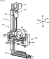
- the cassette transfer robot 17 includes a CZ drive shaft 171 serving as a third shaft and a CS drive shaft 172 serving as a second shaft.
- the CZ drive shaft 171 is configured to move the robot arm 18 serving as a first shaft in the up-down direction (that is, in the Z1-Z2 direction), and the CS drive shaft 172 is configured to move the CZ drive shaft 171 in the left-right direction (that is, in the Y2-Y1 direction).
- the robot arm 18 serves as a movable structure configured to be movable horizontally and movable up and down. Thereby, the robot arm 18 is capable of accessing the cassette 2 at an appropriate position.
- a reflective optical sensor 101 is provided at a base of the robot arm 18, for example, at a lower end of the robot arm 18.
- the reflective optical sensor 101 is provided at the movable structure of the cassette transfer robot 17.
- the reflective optical sensor 101 is not capable of being driven by the robot arm 18. Therefore, the reflective optical sensor 101 is configured to be movable horizontally and movable up and down.
- each of the reflectors 105 may also be referred to as a "reflector 105".
- An opening on a bottom of the cassette 2 placed on the cassette stage device 13 is located at a location where the reflective optical sensor 101 and the reflector 105 face each other. As shown in FIG.
- the reflective optical sensor 101 is provided with a predetermined distance from the cassette 2. Further, the wafer 1 stored in the cassette 2 placed on the cassette stage device 13 is in a vertical state. Further, as shown in FIG. 2 , a plurality of reflectors 106 extending in the X1-X2 direction beside a plurality of wafer alignment holes 53 described later, respectively, are provided at the cassette stage device 13.
- each of the reflectors 106 may also be referred to as a "reflector 106”
- each of the wafer alignment holes 53 may also be referred to as a "wafer alignment hole 53".
- the present embodiments are described by way of an example in which the reflector 105 is provided at the cassette stage device 13, the present embodiments are not limited thereto.
- the reflector 105 may be provided at a movable shutter of a cassette insertion port on a front panel of the apparatus.
- the reflective optical sensor 101 and the reflector 105 will be described with reference to FIG. 4 .
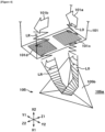
- the reflective optical sensor 101 includes: a light emitter (which is a light emitting structure) 101a configured to emit an outgoing light LO toward the wafer 1 accommodated in the cassette 2; and a light receiver (which is a light receiving structure) 101b configured to receive a reflected light LR obtained by reflecting the outgoing light LO on the reflector 105.
- the light emitter 101a and the light receiver 101b are arranged adjacent to each other and are integrated.
- the reflective optical sensor 101 is configured as a so-called reflective photoelectric sensor.
- the reflective optical sensor 101 includes a polarizing filter 101c provided corresponding to the light emitter 101a and a polarizing filter 101d provided corresponding to the light receiver 101b.
- Polarization directions of the polarizing filter 101c and the polarizing filter 101d are set to be different from each other. That is, according to the present embodiments, the polarization directions may be orthogonal to each other.
- the outgoing light LO By passing through the polarizing filter 101c, the outgoing light LO becomes a linearly polarized light (for example, a wave in the Y1-Y2 direction) vibrating in a direction (first direction), and also becomes a beam-shaped parallel light directed toward the reflector 105. Thereafter, the outgoing light LO is returned and reflected back by the reflector 105 and directed toward the light receiver 101b as the reflected light LR.
- the reflected light LR is a linearly polarized light (for example, a wave in the Z1-Z2 direction) vibrating in a direction (second direction) orthogonal to the outgoing light LO, and can pass through the polarizing filter 101d.
- the polarizing filter 101d is a polarizing filter whose absorption axis is in the first direction.
- the reflective optical sensor 101 is capable of accurately determining (detecting) whether the orientation flats of the wafers 1 are aligned based on a presence or absence of the reflected light LR.
- the reflector 105 is further configured to return and reflect a light whose polarization direction is different from a polarization direction of the incident light incident on the reflector 105 (that is, the outgoing light LO) as the reflected light LR to the light receiver 101b.
- a reflective surface 105a of the reflector 105 is constituted by a plurality of corner cubes 105b which are regularly arranged.
- each of the plurality of corner cubes 105b may also be referred to as a "corner cube 105b".
- the term "corner cube” may refer to a minute hollow whose shape is formed by combining three planes orthogonal to one another, for example.
- the reflector 105 is configured to be capable of returning and reflecting the light. Further, in FIG. 4 , a representative enlarged view of the corner cube 105b is illustrated. Further, the reflector 105 may include a transparent particle substance. The reflector 105 is not limited to the corner cube 105b described above. For example, the reflector 105 may be of any structure capable of rotating the polarization direction of the incident light to a greater extent than the reflected light reflected by the wafer 1.
- the reflector 105 is provided at one end (that is, a first end) of a predetermined optical path LP.
- the predetermined optical path LP is set such that the outgoing light LO from the reflective optical sensor 101 can pass therethrough without hitting the wafer 1 when each of the orientation flats of the wafers 1 is oriented in a predetermined direction (that is, when each of the orientation flats of the wafers 1 is aligned at a predetermined location).
- the optical path LP is perpendicular to the surface of the wafer 1, and a plurality of optical paths including the optical path LP are set for the cassette 2 on the cassette stage device 13.
- the plurality of optical paths including the optical path LP may also be referred to as "optical paths LP".
- two optical paths LP are set in a manner corresponding to the vicinity of both ends of the orientation flat of the wafer 1 aligned in the predetermined direction within the cassette 2.
- three or more optical paths LP may be provided.
- a controller 121 serving as a control structure is configured to be capable of checking whether or not the orientation flats of the wafers 1 are aligned (or oriented) in the predetermined direction by sequentially moving the reflective optical sensor 101 to a plurality of positions corresponding to the optical paths LP.
- the controller 121 is configured to be capable of causing the reflective optical sensor 101 to move to the other end (that is, a second end) of the optical path LP set for the cassette 2 (which is a target to be checked) such that the reflective optical sensor 101 is commonly used for the cassettes 2.
- the outgoing light LO from the light emitter 101a hits the reflector 105, and the reflected light LR returns to the light receiver 101b.
- the outgoing light LO from the light emitter 101a is blocked by the wafers 1 in one of the optical paths LP. Therefore, the outgoing light LO does not reach the reflector 105, and the reflected light LR does not return to the light receiver 101b.
- the outgoing light LO is reflected by the wafers 1 and the outgoing light LO reflected by the wafers 1 returns to the light receiver 101b.
- the outgoing light LO reflected by the wafers 1 cannot pass through the polarizing filter 101d. Therefore, the outgoing light LO reflected by the wafers 1 cannot be detected by the light receiver 101b.
- the wafer 1 whose light transmittance is similar to that of silicon carbide (SiC) is located in the optical path LP, it is detected as a decrease in a light reception level of the light receiver 101b.
- an attenuation of the light reception level due to the wafer 1 with the light transmittance is twice that of a transmissive optical sensor. Thereby, it is possible to preferably increase a detection accuracy of the reflective optical sensor 101 as compared with that of the transmissive optical sensor.
- the present embodiments are described by way of an example in which the wafer 1 is provided with the orientation flat, the present embodiments are not limited thereto.
- the optical path LP is set for each of the cassettes 2 on the cassette stage device 13.
- the reflector 105 is provided for each of the cassettes 2.
- the reflector 105 is provided at the cassette stage device 13 opposite to the reflective optical sensor 101 with the cassette 2 related thereto provided therebetween.
- the cassette stage device 13 is provided with two reflectors 105 in a manner corresponding to the two cassettes 2.
- the controller 121 is configured to be capable of controlling the cassette transfer robot 17 such that the reflective optical sensor 101 is moved to a detection position of the orientation flat or the notch corresponding to a parameter such as a size and a material of the wafer 1. Further, before moving the reflective optical sensor 101, the reflective optical sensor 101 is at a position (which is a home position) shown in FIG. 2 . After it is confirmed that the orientation flats of the wafers 1 are aligned, the reflective optical sensor 101 returns to the home position. On the other hand, since a size of the reflector 105 is set such that the reflector 105 is capable of reflecting the outgoing light LO on the optical path LP for the entire types of the wafers 1 to be handled, it is preferable that the reflector 105 is not moved.
- an output (current value) of the reflective optical sensor 101 is input to the controller 121 via an amplifier 102.
- the amplifier 102 performs a threshold value determination.
- the threshold value is set to a value between a light reception level when the orientation flats of an entirety of silicon carbide (SiC) wafers are aligned and a light reception level when an orientation flat of a single wafer such as a silicon carbide wafer (SiC wafer) whose light transmittance is the highest among wafers to be handled is not aligned.
- the term "when the orientation flat of a single wafer whose light transmittance is the highest is not aligned" may refer to a case where the wafer blocks one or both of the optical paths of the reflective optical sensor 101 through which the light is emitted or received.
- the reflective optical sensor 101 may be moved along the orientation flat in the Y2-Y1 direction or across the edge in the Z1-Z2 direction to determine based on a change in an intensity (that is, a relative value determination may be performed). Further, since the light is scattered at the edge of the wafer, it is possible to obtain a large change in the light reception level even with a wafer whose light transmittance is close to 100 %.
- the controller 121 will be described with reference to FIG. 3 .
- the controller 121 may be constituted by a computer including a CPU (Central Processing Unit) 121a, a RAM (Random Access Memory) 121b, a memory 121c and an I/O port 121d.
- the RAM 121b, the memory 121c and the I/O port 121d may exchange data with the CPU 121a through an internal bus 121e.
- an input/output device 122 constituted by a component such as a touch panel and an external memory 123 are connected to the controller 121.
- the memory 121c is configured by a component such as a flash memory and an HDD (Hard Disk Drive).
- a control program configured to control operations of the substrate processing apparatus 10 and a process recipe (hereinafter, also simply referred to as a "recipe") containing information on sequences and conditions of a substrate processing described later may be readably stored in the memory 121c.
- the recipe is obtained by combining steps of the substrate processing described later such that the controller 121 can execute the steps to acquire a predetermined result, and is a high-level language compared to the control program.
- the control program and the recipe may be collectively or individually referred to as a "program”.
- the memory 121c is configured to sequentially store log information regarding the operations and states of the apparatus.
- the RAM 121b functions as a memory area (work area) where a program or data read by the CPU 121a is temporarily stored.
- the I/O port 121d is connected to the above-described components such as the cassette transfer structure 12, the cassette stage device 13, the wafer posture aligner 14, the cassette transfer robot 17, the wafer transfer device 19, a rotator (not shown), the boat elevator 22 and the amplifier 102.
- the CPU 121a is configured to read the control program from the memory 121c and execute the read control program. Furthermore, the CPU 121a is configured to read the recipe of the substrate from the memory 121c in accordance with an operation command inputted from the input/output device 122. In accordance with the contents of the read recipe, the CPU 121a may be configured to control various operations such as a posture alignment operation of the cassette transfer structure 12, a rotation operation of the cassette stage device 13, an operation of the wafer posture aligner 14, a control operation of the robot arm 18 by the cassette transfer robot 17, a rotation control operation and an elevating and lowering control operation of the wafer transfer device 19, and an elevating and lowering control operation of the boat elevator 22.
- the controller 121 may be embodied by installing the above-described program stored in the external memory 123 into the computer.
- the external memory 123 may include a magnetic disk such as a hard disk and a semiconductor memory such as a USB memory.
- the memory 121c or the external memory 123 may be embodied by a tangible (non-transitory) computer readable recording medium.
- the memory 121c and the external memory 123 may be collectively or individually referred to as a "recording medium".
- the term “recording medium” may refer to the memory 121c alone, may refer to the external memory 123 alone, and may refer to both of the memory 121c and the external memory 123.
- a communication structure such as the Internet and a dedicated line may be used for providing the program to the computer.
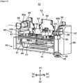
- the cassette transfer structure 12 will be described with reference to FIG. 5 .
- a frame 43 is constituted by fixing a front plate 41 in the X1 direction and a rear plate (not shown) in the X2 direction to a lower portion of a left side plate 38 in a Y2 direction and a right side plate 39 in a Y1 direction.
- a lower portion of the frame 43 is of a rectangular tube shape.
- Two hinge structures 35 are vertically fixed to an outer surface of the right side plate 39 at an end of the right side plate 39 adjacent to the front plate 41.
- Two hinge structures 36 are fixed to a front portion (in the X1 direction) of the housing 11 shown in FIG. 1 , and are connected to the two hinge structures 35 corresponding thereto.
- each of the two hinge structures 35 may also be referred to as a "hinge structure 35”
- each of the two hinge structures 36 may also be referred to as a "hinge structure 36”.
- a rotating shaft 49 is configured to support the placement table 44 on the left side plate 38 and the right side plate 39 so as to be rotatable around a CY axis.
- the placement table 44 includes a pair of rotating plates 45a and 45b, an internal transfer stage 46, an external transfer stage 47 and a lower plate 48.
- Each of the rotating plates 45a and 45b is fixed to the rotating shaft 49 on the CY axis, and is rigidly joined by the lower plate 48 provided between the rotating plates 45a and 45b.
- the placement table 44 is configured to be rotatable around the rotating shaft 49.
- the internal transfer stage 46 is fixed to the rotating plates 45a and 45b and/or the lower plate 48.
- the external transfer stage 47 is attached to the rotating plates 45a and 45b in a horizontal state via a plurality of guides 51 (which is configured to allow a movement in one direction alone) such that the cassette 2 in the vertical posture is movable up and down.
- An air cylinder 52 is provided between the internal transfer stage 46 and the external transfer stage 47, and is configured to drive the external transfer stage 47 up and down.
- the cassette stage device 13 includes a vertical mover.
- the external transfer stage 47 is further configured to be movable in the front-rear direction (X1-X2 direction).
- the two cassettes 2 can be placed on the internal transfer stage 46 or the external transfer stage 47. In other words, each of the internal transfer stage 46 and the external transfer stage 47 is provided with two stages.
- two wafer alignment holes 53 are provided in the external transfer stage 47 with a predetermined interval therebetween.
- the wafer posture aligner 14 is provided at the lower plate 48 below the wafer alignment holes 53.
- a drive structure 65 configured to rotate the rotating shaft 49 is provided at the outer surface of the right side plate 39.
- the drive structure 65 includes components such as an AC servo motor, a worm gear box and a position sensor, and is configured to be capable of rotating the cassette 2 on the placement table 44 by 90 ° between the horizontal posture and the vertical posture.
- the vertical mover of the cassette stage device 13 By the vertical mover of the cassette stage device 13, it is possible to move the external transfer stage 47 between an upper position and a lower position.
- the cassette 2 in the vertical posture (that is, in an upright state) can be rotated by the cassette posture converter.
- the cassette posture aligner that is, the wafer posture aligner 14.
- the optical path LP is arranged in a space provided between the cassette 2 and the wafer posture aligner 14. Thereby, it is possible to check the orientation flat.
- the wafer posture aligner 14 includes a support base 141, a pair of rollers 142a and 142b rotatably spanned over the support base 141 in the horizontal direction, a rotation driver (which is a rotation driving structure) 143 and a stopper 144 provided adjacent to the roller 142b.
- a rotation driver which is a rotation driving structure
- Each of the pair of rollers 142a and 142b extends in a direction in which the wafers stored in the cassette 2 are aligned (that is, in the X1-X2 direction).
- the rotation driver 143 is configured to synchronously rotate the rollers 142a and 142b in the same direction.
- the wafer posture aligner 14 is configured to be movable up and down relative to the cassette 2 placed on the placement table 44.
- the orientation alignment is mechanically performed by rotating the rollers 142a and 142b such that the wafers 1 are rotated once or more and by regulating a rotation of the wafers 1 by the stopper 144 and idling the rollers 142a, 142b when the orientation flats are aligned.
- the orientation alignment includes an up-and-down movement of the external transfer stage 47, it may take several minutes to perform the orientation alignment.
- a notch alignment may be performed in a similar manner.
- a comb-shaped sensor 111 is provided at the wafer posture aligner 14 so as not to mechanically interfere with the cassette 2 placed on the cassette stage device 13.
- the comb-shaped sensor 111 is made of a predetermined material and is configured to detect a presence or absence of the wafer 1 in the cassette 2 before a wafer posture alignment (when the wafer 1 is in the vertical state).
- the comb-shaped sensor 111 is attached to a side surface of the support base 141 adjacent to the roller 142a (in the Y2 direction) so as to be movable up and down relative to the cassette 2.
- the comb-shaped sensor 111 is configured to be movable between a detection position and a retracted position so as to be capable of detecting wafers of any size included in detection parameters described later. Thereby, it is possible to commonly use the comb-shaped sensor 111 for the wafers with different diameters, and it is also possible to improve the versatility.
- a wafer mapping by the comb-shaped sensor 111 is performed in a posture different from that of the cassette 2 in a wafer mapping by the reflective optical sensor 101, which will be described later. That is, it is possible to provide the comb-shaped sensor 111 at a different position from that of the reflective optical sensor 101.
- the comb-shaped sensor 111 is configured as a comb-shaped structure in which a plurality of sensor pairs each including a light emitter and a light receiver are arranged in a number corresponding to the number of the wafers 1 capable of being accommodated in the cassette 2 along an arrangement direction of the wafers 1.
- a light emitting surface of the light emitter of each sensor pair (in which the light emitting surface and a light receiving surface of the light receiver face each other) is positioned such that the presence or absence of each wafer 1 can be detected by each sensor pair.
- the light emitter of each sensor pair is constituted by a light emitting diode
- the light receiver of each sensor pair is constituted by a phototransistor.
- the light emitter of each sensor pair is arranged in a manner corresponding to a side portion of an arrangement area (arrangement region) of the wafer 1, in the present example, corresponding to a side portion of a storage area (slot) for each of the wafers 1 in the cassette 2.
- the light receiver of each sensor pair is arranged on an incident optical path of the light from the light emitter so as to face the light emitter via the storage area for each of the wafer 1.
- the light emitter and the light receiver are arranged such that the light emitting surface of the light emitter faces a first surface of the wafer 1 and the light receiving surface of the light receiver faces a second surface of the wafer 1 opposite to the first surface.
- the comb-shaped sensor 111 is configured as a transmission type sensor configured to irradiate the wafer 1 with a reference light and configured to detect the light passing through the wafer 1.
- the wafer 1 is configured as a non-transparent wafer (for example, a silicon wafer)
- the light receiver of each sensor pair receives (detects) the light (that is, the reference light) emitted from the light emitter of each sensor pair when the wafer 1 is not present, and the light receiver of each sensor pair does not receive (detect) the light (that is, the reference light) emitted from the light emitter of each sensor pair when the wafer 1 is present. Thereby, it is possible to detect the presence or absence of the wafer 1.
- the presence or absence of the wafer 1 is actually determined by a threshold value processing (which is designed for the silicon wafer) of an amount of the light received by the light receiver of each sensor pair.
- a threshold value processing which is designed for the silicon wafer
- the wafer 1 is configured as a transparent wafer (for example, a quartz wafer)
- since an amount of the light transmitted by the transparent wafer exceeds a threshold value it is not possible to determine the presence or absence of the wafer 1.
- the wafer 1 is configured as a wafer such as the SiC wafer whose light transmittance is about in the middle between that of the silicon wafer and that of the quartz wafer, it is not possible to guarantee a detection of the SiC wafer.
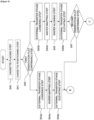
- a substrate processing method using the reaction tube 31 of the processing apparatus 10 will be described with reference to FIGS. 7A and 7B .
- the substrate processing method mentioned above will be described by way of an example in which a step in a manufacturing process of a semiconductor device (for example, a film forming process in which a film is formed on the wafer 1) is performed by using the reaction tube 31 of the processing apparatus 10 described above.
- the operations of components constituting the processing apparatus 10 are controlled by the controller 121.
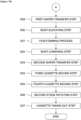
- the wafers (which is unprocessed) 1 are charged (loaded) into the cassette 2. Then, the cassette 2 is transferred to the front of the housing 11 by the external transfer device (not shown) and is placed on the cassette stage device 13 of the cassette transfer structure 12. The wafers 1 in the cassette 2 are in the vertical state. When the cassette 2 is placed on the cassette stage device 13, the external transfer stage 47 of the cassette stage device 13 is at the upper position.
- an orientation flat confirmation is performed using the reflective optical sensor 101.
- the orientation flat confirmation is performed by moving the reflective optical sensor 101 to positions corresponding to the two optical paths LP.
- a wafer aligning step S22 is performed.
- an orientation flat alignment that is, the wafer aligning step S22
- a step S24 is performed.
- the wafers 1 are aligned by the wafer posture aligner 14 using the orientation flats.
- the orientation flat confirmation is performed by the reflective optical sensor 101, similarly to the step S21.
- the step S24 is performed.
- the step S22 is performed again, and a wafer alignment is retried.
- a step S38 is performed. Further, before performing the step S38, another retry may be performed by moving the optical path of the reflective optical sensor 101 slightly downward (by lowering an accuracy of the orientation flat alignment.
- the cassette stage device 13 by rotating the cassette stage device 13 by 90 °, the cassette 2 is rotated by 90 °. Thereby, the wafers 1 in the cassette 2 are in a horizontal state.
- the reflective optical sensor 101 is moved to a position behind the reflector 106 of the cassette stage device 13 (in the X2 direction). Then, by elevating the robot arm 18 using the CZ drive shaft 171, the reflective optical sensor 101 scans the cassette 2 from the bottom to the top (with a resolution of 0.05 mm).
- the reflector 106 is substantially the same structure as the reflector 105, and faces the opening on the bottom of the cassette 2 facing the external transfer stage 47.
- the reflector 106 is provided near the wafer alignment holes 53 of the external transfer stage 47 so as not to interfere with the operation of the wafer posture aligner 14. Thereby, it is possible to ensure the optical path between the reflective optical sensor 101 and the reflector 106.
- a received light intensity (amount of the light) is low at a location where the wafer 1 is present, and the received light intensity is high at a location where the wafer 1 is not present.
- Such a received light intensity is acquired as scan data.
- a slot width of the cassette 2 is greater than a thickness of the wafer 1, there are locations where the wafer 1 is not present even within the slot.
- the presence (“ON”) and absence (“OFF”) of the wafer 1 and an abnormality of the wafer 1 in each slot are determined based on the detection data for each slot. When there is no detection data or when the position or the thickness in the Z1-Z2 direction does not fall within a tolerance range, it is determined that the slot is abnormal.
- step S25 When it is determined in the step S25 that there is an abnormality, the step S38 is performed. When it is determined in the step S25 that there is no abnormality, a step S27 is performed.
- the cassette 2 is held (supported) by the hand 173 of the robot arm 18, and the cassette 2 is transferred to the cassette shelf 15 or the spare cassette shelf 16 by the hand 173 of the robot arm 18.
- the cassette 2 is transferred by the hand 173 of the robot arm 18 from the cassette shelf 15 or the spare cassette shelf 16 to a transfer shelf located at a position facing the wafer transfer device 19 of the cassette shelf 15. Then, a step S29 in FIG. 7B is performed.
- the wafers 1 in the cassette 2 are in the horizontal state, and the wafers 1 in the cassette 2 placed on the transfer shelf are transferred and loaded into the boat 25 by the wafer transfer device 19.
- the boat 25 is loaded into the reaction tube 31 by the boat elevator 22.
- an inner atmosphere of the process chamber 32 is controlled such that an inner pressure of the process chamber 32 reaches and is maintained at a predetermined pressure. Further, an inside of the process chamber 32 is controlled such that an inner temperature of the process chamber 32 reaches and is maintained at predetermined temperature using a heater. For example, a source gas and a reactive gas are supplied into the process chamber 32 to form the film on the wafer 1.
- the boat 25 is taken out from the reaction tube 31 by the boat elevator 22 (that is, the boat 25 is unloaded).
- the wafers 1 (which are processed) in the boat 25 are transferred into the cassette 2 on the transfer shelf by the wafer transfer device 19.
- the cassette 2 on the transfer shelf is transferred to the cassette shelf 15 or the spare cassette shelf 16 by the hand 173 of the robot arm 18.
- the cassette 2 When the cassette 2 is transferred (unloaded) out of the processing apparatus 10, the cassette 2 is transferred from the cassette shelf 15 or the spare cassette shelf 16 to the cassette stage device 13 of the cassette transfer structure 12 using the hand 173 of the robot arm 18.
- the cassette 2 is rotated by 90 ° by the cassette stage device 13, an access port of the cassette 2 is rotated to an upward posture, and the wafers 1 are in the vertical state.
- the cassette 2 is taken out and transferred outside the housing 11 by the external transfer device.
- a modified example of the substrate processing step of the processing apparatus will be described with reference to FIG. 9 .
- the wafers (which is unprocessed) 1 are charged (loaded) into the cassette 2. Then, the cassette 2 is transferred to the front of the housing 11 by the external transfer device (not shown) and is placed on the cassette stage device 13 of the cassette transfer structure 12. The wafers 1 in the cassette 2 are in the vertical state. When the cassette 2 is placed on the cassette stage device 13, the external transfer stage 47 of the cassette stage device 13 is at the home position.
- the external transfer stage 47 moves backward (in the X2 direction) to press (dock) the cassette 2 placed on the cassette stage device 13 against the internal transfer stage 46 in the upright state so as to position the cassette 2.
- the orientation flats of the wafers 1 stored in the cassette 2 is confirmed by the reflective optical sensor 101.
- a step S43a is performed.
- a step S43b is performed.
- the external transfer stage 47 is lowered to the lower position.
- the wafer mapping is performed by using the comb-shaped sensor 111 to detect the presence or absence of the wafer 1 in the cassette 2 for each slot.
- the external transfer stage 47 is elevated to the home position. Then, the step S24 (shown in FIG. 7A ) of the embodiments described above is performed.
- the material of the wafer 1 is determined to be silicon (Si). Further, when it is determined to be “ON” in the wafer mapping by the reflective optical sensor 101 and when it is determined to be “OFF” in the wafer mapping by the comb-shaped sensor 111, the material of the wafer 1 is determined to be silicon carbide (SiC). Further, when it is determined to be “OFF” in the wafer mapping by the reflective optical sensor 101 and when it is determined to be “OFF” in the wafer mapping by the comb-shaped sensor 111, it is determined that the wafer 1 is not present.
- the external transfer stage 47 is lowered to the lower position.
- the wafer mapping is performed by using the comb-shaped sensor 111.
- the wafers 1 are aligned by the wafer posture aligner 14 using the orientation flats.
- the external transfer stage 47 is elevated to the home position.
- the orientation flat confirmation is performed using the reflective optical sensor 101.
- the step S24 (shown in FIG. 7A ) of the embodiments described above is performed.
- the step S38 (shown in FIG. 7A ) of the embodiments described above is performed.
- the material of the wafer 1 may be determined by integrating detection results of the comb-shaped sensor 111 in the step S44a or the step S44b.
- the wafer 1 when the wafer 1 is detected by both of the comb-shaped sensor 111 and the reflective optical sensor 101, it is possible to determine that the wafer 1 is a non-transparent wafer such as the silicon wafer, and when the wafer 1 is detected by the reflective optical sensor 101 alone, it is possible to determine that the wafer 1 is a transparent wafer such as the SiC wafer.
- the embodiments and the modified example mentioned above are described by way of an example in which a batch type substrate processing apparatus capable of simultaneously processing a plurality of substrates is used to form the film.
- the technique of the present disclosure is not limited thereto.
- the technique of the present disclosure may be preferably applied when a single wafer type substrate processing apparatus capable of simultaneously processing one or several substrates is used to form the film.
- the embodiments and the modified example mentioned above are described by way of an example in which a substrate processing apparatus including a hot wall type process furnace is used to form the film.
- the technique of the present disclosure is not limited thereto.
- the technique of the present disclosure may be preferably applied when a substrate processing apparatus including a cold wall type process furnace is used to form the film.
- a technique that includes: a stage where a cassette accommodating substrates is placed, wherein the substrates are provided with orientation indicators; a reflector provided at a first end of an optical path set to enable a light to pass therethrough without hitting the substrates when the orientation indicators of the substrates are oriented in a predetermined direction; a robot configured to transfer the cassette between the stage and a shelf, and including a reflective optical sensor configured to emit the light along the optical path and to detect the light reflected from the reflector; and a controller controlling the robot to move the reflective optical sensor to a position corresponding to the optical path when checking whether the orientation indicators of the substrates on the stage are aligned in the predetermined direction.
Landscapes
- Engineering & Computer Science (AREA)
- Robotics (AREA)
- Mechanical Engineering (AREA)
- Physics & Mathematics (AREA)
- General Physics & Mathematics (AREA)
- Human Computer Interaction (AREA)
- Life Sciences & Earth Sciences (AREA)
- General Life Sciences & Earth Sciences (AREA)
- Geophysics (AREA)
- Container, Conveyance, Adherence, Positioning, Of Wafer (AREA)
- Manipulator (AREA)
Applications Claiming Priority (1)
| Application Number | Priority Date | Filing Date | Title |
|---|---|---|---|
| JP2023107930A JP2025006889A (ja) | 2023-06-30 | 2023-06-30 | 基板カセット取扱い装置、基板処理装置、基板処理方法、半導体装置の製造方法およびプログラム |
Publications (2)
| Publication Number | Publication Date |
|---|---|
| EP4498412A2 true EP4498412A2 (de) | 2025-01-29 |
| EP4498412A3 EP4498412A3 (de) | 2025-03-12 |
Family
ID=91530330
Family Applications (1)
| Application Number | Title | Priority Date | Filing Date |
|---|---|---|---|
| EP24181814.5A Pending EP4498412A3 (de) | 2023-06-30 | 2024-06-12 | Substratkassettenhandhabungsvorrichtung, substratverarbeitungsvorrichtung, substratverarbeitungsverfahren und programm |
Country Status (6)
| Country | Link |
|---|---|
| US (1) | US20250006526A1 (de) |
| EP (1) | EP4498412A3 (de) |
| JP (1) | JP2025006889A (de) |
| KR (1) | KR20250003306A (de) |
| CN (1) | CN119230445A (de) |
| TW (1) | TW202505688A (de) |
Citations (1)
| Publication number | Priority date | Publication date | Assignee | Title |
|---|---|---|---|---|
| JP2002270675A (ja) | 2001-03-06 | 2002-09-20 | Hitachi Kokusai Electric Inc | 基板処理装置 |
Family Cites Families (4)
| Publication number | Priority date | Publication date | Assignee | Title |
|---|---|---|---|---|
| JP2003243487A (ja) * | 2002-02-20 | 2003-08-29 | Hitachi Kokusai Electric Inc | 基板処理装置 |
| JP4276440B2 (ja) * | 2003-01-06 | 2009-06-10 | 東京エレクトロン株式会社 | 基板検出方法及び装置並びに基板処理装置 |
| JP4575727B2 (ja) * | 2004-08-23 | 2010-11-04 | 川崎重工業株式会社 | 基板状態検出装置、ロボットハンド及び基板搬送用ロボット |
| US11295975B2 (en) * | 2019-09-13 | 2022-04-05 | Brooks Automation Us, Llc | Method and apparatus for substrate alignment |
-
2023
- 2023-06-30 JP JP2023107930A patent/JP2025006889A/ja active Pending
-
2024
- 2024-05-30 CN CN202410685129.4A patent/CN119230445A/zh active Pending
- 2024-06-10 KR KR1020240074965A patent/KR20250003306A/ko active Pending
- 2024-06-12 US US18/740,730 patent/US20250006526A1/en active Pending
- 2024-06-12 EP EP24181814.5A patent/EP4498412A3/de active Pending
- 2024-06-17 TW TW113122312A patent/TW202505688A/zh unknown
Patent Citations (1)
| Publication number | Priority date | Publication date | Assignee | Title |
|---|---|---|---|---|
| JP2002270675A (ja) | 2001-03-06 | 2002-09-20 | Hitachi Kokusai Electric Inc | 基板処理装置 |
Also Published As
| Publication number | Publication date |
|---|---|
| JP2025006889A (ja) | 2025-01-17 |
| EP4498412A3 (de) | 2025-03-12 |
| TW202505688A (zh) | 2025-02-01 |
| KR20250003306A (ko) | 2025-01-07 |
| US20250006526A1 (en) | 2025-01-02 |
| CN119230445A (zh) | 2024-12-31 |
Similar Documents
| Publication | Publication Date | Title |
|---|---|---|
| JP5949741B2 (ja) | ロボットシステム及び検出方法 | |
| KR102291970B1 (ko) | 기판 처리 장치, 위치 편차 보정 방법 및 기억 매체 | |
| US5813819A (en) | Substrate transfer apparatus, and method of transferring substrates | |
| TWI362081B (de) | ||
| EP0836225A1 (de) | Substratversetzungsapparat und system für thermische behandlungen, wobei dieser apparat angewendet wird | |
| US20130204425A1 (en) | Thermal processing apparatus, thermal processing method, and storage medium | |
| CN107680928B (zh) | 示教夹具、基板处理装置以及示教方法 | |
| KR101690229B1 (ko) | 기판 반송 방법, 기판 반송 장치 및 기억 매체 | |
| US8386064B2 (en) | Control device and control method | |
| TWI288445B (en) | Substrate transfer apparatus and method, and storage medium | |
| EP4498412A2 (de) | Substratkassettenhandhabungsvorrichtung, substratverarbeitungsvorrichtung, substratverarbeitungsverfahren und programm | |
| JP4468159B2 (ja) | 基板処理装置及びその搬送位置合わせ方法 | |
| KR20090069544A (ko) | 카세트 로딩 장치 및 카세트 로딩 방법 | |
| US11908717B2 (en) | Transfer method and transfer system for transferring substrate between transfer device and substrate stage | |
| JP2005285799A (ja) | カセット内基板位置検出装置、ならびにそれを用いた基板搬出装置および基板処理装置 | |
| JP2008028206A (ja) | 半導体製造装置およびボート載置台 | |
| US20260018440A1 (en) | Substrate Processing Apparatus, Mapping Apparatus, Substrate Processing Method, Method of Manufacturing Semiconductor Device and Non-transitory Computer-readable Recording Medium | |
| JP5050524B2 (ja) | ワイヤーカセットの検査方法、検査装置、ローダー装置及びアンローダー装置 | |
| US20250303561A1 (en) | Transfer robot teaching system and transfer robot teaching method | |
| KR102947038B1 (ko) | 기판 처리 장치 및 촬상 방법 | |
| JPH0936201A (ja) | 基板移載方法および基板移載装置 | |
| JP2026058368A (ja) | マッピング装置、基板処理装置、マッピング方法、半導体装置の製造方法およびプログラム | |
| JP2025157931A (ja) | サンプル測定装置 | |
| KR20080058615A (ko) | 기판 감지 장치 및 기판 감지 시스템 | |
| CN120674362A (zh) | 基板处理装置、基板落下防止机构、基板处理方法、半导体器件的制造方法及程序产品 |
Legal Events
| Date | Code | Title | Description |
|---|---|---|---|
| PUAI | Public reference made under article 153(3) epc to a published international application that has entered the european phase |
Free format text: ORIGINAL CODE: 0009012 |
|
| STAA | Information on the status of an ep patent application or granted ep patent |
Free format text: STATUS: THE APPLICATION HAS BEEN PUBLISHED |
|
| AK | Designated contracting states |
Kind code of ref document: A2 Designated state(s): AL AT BE BG CH CY CZ DE DK EE ES FI FR GB GR HR HU IE IS IT LI LT LU LV MC ME MK MT NL NO PL PT RO RS SE SI SK SM TR |
|
| PUAL | Search report despatched |
Free format text: ORIGINAL CODE: 0009013 |
|
| AK | Designated contracting states |
Kind code of ref document: A3 Designated state(s): AL AT BE BG CH CY CZ DE DK EE ES FI FR GB GR HR HU IE IS IT LI LT LU LV MC ME MK MT NL NO PL PT RO RS SE SI SK SM TR |
|
| RIC1 | Information provided on ipc code assigned before grant |
Ipc: H01L 21/67 20060101ALI20250203BHEP Ipc: H01L 21/68 20060101ALI20250203BHEP Ipc: H01L 21/677 20060101AFI20250203BHEP |
|
| P01 | Opt-out of the competence of the unified patent court (upc) registered |
Free format text: CASE NUMBER: APP_5845/2025 Effective date: 20250218 |
|
| STAA | Information on the status of an ep patent application or granted ep patent |
Free format text: STATUS: REQUEST FOR EXAMINATION WAS MADE |
|
| 17P | Request for examination filed |
Effective date: 20250912 |