EP4492125A2 - Abtastspiegelsysteme und herstellungsverfahren - Google Patents
Abtastspiegelsysteme und herstellungsverfahren Download PDFInfo
- Publication number
- EP4492125A2 EP4492125A2 EP24208450.7A EP24208450A EP4492125A2 EP 4492125 A2 EP4492125 A2 EP 4492125A2 EP 24208450 A EP24208450 A EP 24208450A EP 4492125 A2 EP4492125 A2 EP 4492125A2
- Authority
- EP
- European Patent Office
- Prior art keywords
- platform
- scanning micromirror
- scanning
- micromirror system
- axis
- Prior art date
- Legal status (The legal status is an assumption and is not a legal conclusion. Google has not performed a legal analysis and makes no representation as to the accuracy of the status listed.)
- Pending
Links
Images









Classifications
-
- G—PHYSICS
- G02—OPTICS
- G02B—OPTICAL ELEMENTS, SYSTEMS OR APPARATUS
- G02B26/00—Optical devices or arrangements for the control of light using movable or deformable optical elements
- G02B26/08—Optical devices or arrangements for the control of light using movable or deformable optical elements for controlling the direction of light
- G02B26/10—Scanning systems
- G02B26/101—Scanning systems with both horizontal and vertical deflecting means, e.g. raster or XY scanners
-
- G—PHYSICS
- G02—OPTICS
- G02B—OPTICAL ELEMENTS, SYSTEMS OR APPARATUS
- G02B26/00—Optical devices or arrangements for the control of light using movable or deformable optical elements
- G02B26/08—Optical devices or arrangements for the control of light using movable or deformable optical elements for controlling the direction of light
- G02B26/0816—Optical devices or arrangements for the control of light using movable or deformable optical elements for controlling the direction of light by means of one or more reflecting elements
- G02B26/0833—Optical devices or arrangements for the control of light using movable or deformable optical elements for controlling the direction of light by means of one or more reflecting elements the reflecting element being a micromechanical device, e.g. a MEMS mirror, DMD
- G02B26/085—Optical devices or arrangements for the control of light using movable or deformable optical elements for controlling the direction of light by means of one or more reflecting elements the reflecting element being a micromechanical device, e.g. a MEMS mirror, DMD the reflecting means being moved or deformed by electromagnetic means
-
- G—PHYSICS
- G02—OPTICS
- G02B—OPTICAL ELEMENTS, SYSTEMS OR APPARATUS
- G02B26/00—Optical devices or arrangements for the control of light using movable or deformable optical elements
- G02B26/08—Optical devices or arrangements for the control of light using movable or deformable optical elements for controlling the direction of light
- G02B26/0816—Optical devices or arrangements for the control of light using movable or deformable optical elements for controlling the direction of light by means of one or more reflecting elements
- G02B26/0833—Optical devices or arrangements for the control of light using movable or deformable optical elements for controlling the direction of light by means of one or more reflecting elements the reflecting element being a micromechanical device, e.g. a MEMS mirror, DMD
- G02B26/0858—Optical devices or arrangements for the control of light using movable or deformable optical elements for controlling the direction of light by means of one or more reflecting elements the reflecting element being a micromechanical device, e.g. a MEMS mirror, DMD the reflecting means being moved or deformed by piezoelectric means
-
- G—PHYSICS
- G02—OPTICS
- G02B—OPTICAL ELEMENTS, SYSTEMS OR APPARATUS
- G02B27/00—Optical systems or apparatus not provided for by any of the groups G02B1/00 - G02B26/00, G02B30/00
- G02B27/01—Head-up displays
- G02B27/017—Head mounted
- G02B27/0172—Head mounted characterised by optical features
Definitions
- optical scanning systems may comprise one or more scanning micromirror devices, useful for projecting and scanning a beam of light.
- two scanning micromirror devices may be used in sequence, a first scanning micromirror device for scanning along a first direction, and a second scanning micromirror device, in optical communication with the first scanning micromirror device, for scanning along a second direction.
- a hermetic packaging can enclose a scanning micromirror device for maintaining a lower pressure at the scanning micromirror device inside the hermetic packaging than outside the hermetic packaging.
- an optical relay may be used for providing optical communication between the first scanning micromirror device and the second scanning micromirror device.
- Example optical relays include, but are not limited to, those described by U.S. Provisional Application No. 62/964,508, filed on January 22, 2020 , hereby incorporated by reference.
- An optical scanning system may include a light source arranged to direct emitted light to the first reflector of the first scanning micromirror device.
- the light source can be modulatable to allow for control over color and/or intensity as a function of time and/or the projected position of the light reflected from the scanning micromirror devices to allow for image display.
- Scanning micromirror devices of this aspect may use thick platforms, in some cases.
- a thick platform may allow for the reflector of the micromirror device to be robust and have a good flatness despite inclusion of other components in the platform.
- the first platform may have a thickness of from 100 ⁇ m to 500 ⁇ m.
- Use of a stress relief layer may also enhance the flatness of the reflector, by allowing stresses on different sides of the platform to offset one another, resulting in a good flatness of the reflector.
- the stress relief layer provides a first stress distribution on the first side of the first platform while the first conducting coil provides a second stress distribution on the second side of the first platform.
- the first stress distribution and the second stress distribution may oppose one another and result in at least partially offsetting one another.
- the first conducting coil may be embedded into the second side of the first platform (e.g., positioned in a trench or trenches on the first platform), or it may be position over and supported by the second side of the first platform (e.g., as a partial overlayer).
- the scanning micromirror devices may be actuated using electromagnetic actuation, such as where a current passing through a conducting coil interacts with a magnetic field and where the current is oscillatory in nature to drive oscillatory forces and/or oscillations of the platform.
- the first magnetic field source may be arranged to provide the first magnetic field oriented orthogonal to the first axis.
- Scanning micromirror devices may further comprise a plurality of conductive traces on the plurality of support flexures, such as for providing electrical communication with a conducting coil.
- the conductive traces may apply strain on the support flexures, so it may be desirable for the of conductive traces to be arranged on the plurality of support flexures in a configuration to apply opposite stresses on different sides of the plurality of first support flexures, which may be useful for avoiding, reducing, or limiting nonlinear effects.
- a scanning micromirror device may further comprise one or more piezoelectric actuators arranged to apply forces to oscillate the first platform about the first axis or to sense oscillation or position of the first platform about the first axis.
- Another example scanning micromirror device comprises a first frame coupled to a second base by a plurality of second support flexures, such as where the first frame is oscillatable about a second axis; a second platform coupled to the first frame, such as where the second platform is oscillatable about the second axis together with the first frame; a second reflector positioned on the second platform; a second conducting coil positioned on the first frame, the second conducting coil arranged to apply magnetic forces to the first frame about the second axis; and a second magnetic field source arranged to apply a second magnetic field to the first frame.
- Useful scanning micromirror devices include, but are not limited to, those having a natural resonant frequency of 15 Hz to about 2 kHz.
- a scanning micromirror device may further comprise a second frame coupled between the first frame and the second platform, such as where the second frame is coupled to the first frame by a plurality of third support flexures and where the second frame is oscillatable about the second axis together with the first frame and the second platform.
- such an intermediate frame can include other components, such as sensors or actuators.
- a scanning micromirror device may further comprise a temperature sensor incorporated in the second frame.
- a second scanning micromirror device may further comprise a strain sensor incorporated in the second frame.
- a scanning micromirror device may further comprise a plurality of piezoelectric actuators incorporated in the second frame, such as piezoelectric actuators that are arranged to alter or sense a position of the second platform about a third axis orthogonal to the second axis or to alter or sense a curvature of the second platform.
- An example method comprises providing a two-dimensional optical scanning system, such as a two-dimensional optical scanning system comprising a first scanning micromirror device and a second scanning micromirror device in optical communication with the first scanning micromirror device; inducing a first oscillation of the first scanning micromirror device at a first frequency; inducing a second oscillation of the second scanning micromirror device at a second frequency, such as where the second frequency is optionally smaller than the first frequency; and illuminating a first reflector of the first scanning micromirror device with a light source to generate reflected light that is directed to the second scanning micromirror device and reflected by a second reflector of the second scanning micromirror device to generate output reflected light.
- a two-dimensional optical scanning system such as a two-dimensional optical scanning system comprising a first scanning micromirror device and a second scanning micromirror device in optical communication with the first scanning micromirror device
- the first and second scanning micromirror devices may independently correspond to different scanning micromirror devices described herein.
- methods of this aspect may further comprise directing the output reflected light from the second scanning micromirror device to an eyepiece.
- Methods of this aspect may further comprise synchronously controlling oscillation of the first scanning micromirror device, oscillation of the second scanning micromirror device, and output color and/or intensity of light from the light source. Such a configuration may be useful for drawing an image or image field as well as a sequence of images or image fields.
- An example head-mounted display system may comprise a two-dimensional optical scanning system; and an eyepiece comprising one or more optical components configured to receive and redirect light reflected or output from the two-dimensional optical scanning system to one or two eyes of a user.
- a head mounted display system may include control circuitry operatively coupled to a light source and scanning micromirror device(s) of the two-dimensional optical scanning system, to allow for display of images.
- control circuitry may be configured to display one or more images by synchronously: controlling the light source to emit light corresponding to pixels of the one or more images; controlling current flow in a first conducting coil of a first scanning micromirror device to induce oscillation of the first scanning micromirror device or a platform thereof; and controlling current flow in a second conducting coil of a second scanning micromirror device to induce oscillation of the second scanning micromirror device or a platform thereof.
- the disclosed two-dimensional optical scanning systems can incorporate a first scanning micromirror device oscillating at a relatively higher frequency, which directs reflected light onto a second scanning micromirror device oscillating at a relatively lower frequency, which directs reflected light for projection.
- the disclosed scanning micromirror devices exhibit features providing benefits for two-dimensional optical scanning and image projection.
- some of the scanning micromirror devices are constructed to achieve a high degree of flatness of the reflective element of the scanning mirror, while allowing for good or precise control over the oscillation of the scanning micromirror.
- Some of the scanning micromirror devices can incorporate sensor elements and control elements to allow for monitoring of conditions, like temperature, strain or position.
- Some of the scanning micromirror devices can incorporate actuators, such as for altering a relative position of a reflective element or to change or achieve a high or higher degree of flatness.
- the disclosed scanning micromirror devices can employ electromagnetic actuation, where a conducting coil is position on a platform of the scanning micromirror devices to apply magnetic forces to induce oscillation of the scanning micromirror devices.
- the disclosed scanning micromirror devices can be very thick, such as thicker than conventional scanning micromirror devices, which may allow for improved flatness of reflectors on platforms of the scanning micromirror devices.
- the thickness of the platform of the scanning micromirror device may be in the range from 100 ⁇ m to 500 ⁇ m, such as from 100 ⁇ m to 150 ⁇ m, from 150 ⁇ m to 200 ⁇ m, from 200 ⁇ m to 250 ⁇ m, from 250 ⁇ m to 300 ⁇ m, from 300 ⁇ m to 350 ⁇ m, from 350 ⁇ m to 400 ⁇ m, from 400 ⁇ m to 450 ⁇ m, from 450 ⁇ m to 500 ⁇ m, or any value between the indicated ranges.
- thicker platforms may increase the power requirements for driving oscillation, though operation at a natural resonance can limit the power requirements.
- the increased power requirements can be offset by the ability to maintain flatness of the reflector, which could otherwise result in undesirable image or projection artifacts.
- the disclosed scanning micromirror devices can be used for image projection, such as for projecting light for viewing by a user.
- the disclosed scanning micromirror devices and image projection systems are useful for head-mounted display devices, such as due to their compact size and ability to project high quality images using low power operation.
- FIG. 1 provides a schematic illustration of an example image projection system 100.
- Image projection system 100 comprises a first scanning micromirror device 105, including a first reflector 110, and a second scanning micromirror device 115, including a second reflector 120.
- Image projection system 100 also includes a light source 125 arranged in optical communication with first reflector 110 to direct light 130 from light source 125 to first reflector 110, where it is reflected towards second reflector 120 and, from there, output for projection. Motion of the first scanning micromirror device 105 and the second scanning micromirror device 115 can be driven in such a way to direct output reflected light 130 to a projection plane 135.
- the output reflected light 140 can generate an image at projection plane 135. With repeated scanning, a sequence of images and/or video may be projected.
- the first scanning micromirror device 105 can oscillate about a first axis so that output reflected light 140 can form a series of horizontal (left-to-right and right-to-left) passes, while the second scanning micromirror device 115 can oscillate about a second axis so that output reflected light 140 can also oscillate vertically from top-to-bottom and/or from bottom-to-top across projection plane 135.
- the oscillation frequency along the horizontal direction can be very fast, such as in the range from 1 kHz to 10 MHz, for example.
- Some projection systems may use an oscillation pattern along the vertical direction that is a sawtooth or triangular shape, which can be useful for creating regularly spaced horizontal passes in one vertical direction (e.g., from top-to-bottom), though sinusoidal oscillations patterns may also be used.
- the oscillation frequency along the vertical direction can be slower, such as in the 15 Hz to 2 kHz range, for example.
- a blanking period can be used where no light is generated by light source 125 while the second scanning micromirror device 115 oscillates in the upward direction. In some cases, however, both top-to-bottom and bottom-to-top projections can be used. Blanking periods can also be used on the extremes of the horizontal dimension to avoid projection at the side edges of projection plane 135.
- Image projection system 100 can be a component of an optical projector, for example, which can be used to project still images or video images at a projection plane.
- the image projection system 100 can be a component of a head-mounted display device and/or used to couple projected light into an eyepiece, such as an eyepiece of a head-mounted display device.
- Projection plane 135 may correspond to an eyepiece or a user's retina, in some examples.
- Image projection system 100 can optionally include projection optics, such as mirrors, lenses, collimators, filters, gratings, or the like, which are not illustrated in FIG. 1 , but can be positioned in the optical path between the light source 125 and the projection plane 135, for example.
- an optical relay 145 such as comprising multiple reflective and/or focusing elements, can be used between the first scanning micromirror device 105 and the second scanning micromirror device 115 to direct light reflected from the first mirror 110 onto the second mirror 120.
- Light source 125 can be a single or multi-color light source and can include a light emitting diode or laser source, for example, which can be output switchable or modulatable at a high rate, such as up to 100 MHz, for example.
- light source 125 can comprise or correspond to multiple individually modulatable light sources, such as outputting different colors (e.g., red, green, blue).
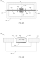
- base 205 is depicted in FIG. 2A as a frame surrounding other components, base 205 may extend in other directions or be positioned differently with respect to platform 210, such as beneath first platform 210, for example.
- a reflector 225 may be positioned on the opposite surface of platform 210 as that shown in FIG. 2A .
- Scanning micromirror device 200 also includes conductive trace 230, which forms a conductive coil 235 at platform 210.
- Conductive coil 235 can be used for applying forces (e.g., magnetic/electromagnetic forces) to platform 210 to induce oscillation of platform 210 about axis 220.
- Conductive coil 235 can have any suitable number of turns.
- the conductive traces 230 which provide a way to pass current from a current source via contacts 240 to conductive coil 235, can add to the stiffness of the support flexures 215.
- the conductive traces 230 can be positioned both on the side of scanning micromirror device 200 shown in FIG. 2A , as well as on the opposite side, to counterbalance the perturbations.
- other actuators such as piezoelectric actuators, electrostatic actuators, or the like.
- piezoelectric actuators or electrostatic actuators can be used for sensing a position, scan angle, or oscillation, of platform 210.
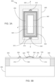
- FIG. 2B shows a schematic cross-sectional view of an example scanning micromirror device 200.
- axis 220 extends in and out of the plane, with oscillation of platform 210 shown schematically by arrow 245.
- a magnetic source 250 is shown, positioned to provide a magnetic field at platform 210. The magnetic field can interact with current flowing through conductive coil 235 for imparting forces on platform 210 to induce oscillation, such as by passing an alternating current through conductive coil 235.
- other forms of actuators such as piezoelectric actuators or electrostatic actuators can be used.
- Reflector 225 is shown on the opposite side of platform 210. Reflector 225 may comprise a metal reflector or a dielectric reflector, or a combination, for example.
- conductive coil 235 may apply stresses to platform 210, which can result in perturbations to the flatness of reflector 225.
- a stress relief layer 255 may be positioned between reflector 225 and platform 210. Stress relief layer 255 can apply stresses to platform 210 opposite those of conductive coil 235. Stress relief layer 255 and conductive coil 235 may be the same material and/or may have the same volume on platform 210 to minimize or reduce the total applied stresses and limit the perturbations to the flatness of reflector 225.
- the configuration of scanning micromirror device 200 may be useful for relatively high frequency oscillation, such as in the range from 1 kHz to 10 MHz, for example.
- the device may be operated at its resonant frequency, which can result in a quality factor (Q), which can amplify the displacement achieved through actuation.
- Q quality factor
- the natural resonant frequency for oscillation of platform 210 about axis 220 may be in the range from 1 kHz to 10 MHz.
- FIG. 2C shows a cross sectional schematic illustration of a scanning micromirror device 200 including a vacuum packaging.
- Vacuum packaging may include a transparent top component 260 and a bottom component 265.
- Top component 260 may be transparent, so as to allow light transmission therethrough, and may optionally include an antireflective coating on one or more surfaces to minimize surface reflections.
- Example materials for top component 260 may include glass or crystalline materials.
- Bottom component 265 can be positioned adjacent to magnetic source 250, and can comprise a transparent or non-transparent material. In some examples, bottom component 265 can comprise silicon.
- Top component 260 and bottom component 265 may be sealed against base 205, such as using glass frit paste.
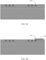
- FIG. 3A and FIG. 3B provide a top and cross-sectional schematic illustrations, respectively, of another example scanning micromirror device 300.
- Scanning micromirror device 300 can comprise silicon or other materials, allowing patterning and fabrication according to known microfabrication techniques.
- Scanning micromirror device 300 includes a base 305, a first frame 310, which is coupled to base 305 by a plurality of support flexures 315.
- Support flexures 315 are constructed and arranged to allow for oscillation of first frame 310, and internal or associated components, about axis 320, as shown schematically by arrow 345.
- Scanning micromirror device 300 also includes a platform 325 and a second frame 330 positioned between platform 325 and first frame 310.
- a conductive coil 335 is shown positioned on first frame 310, and a reflector 340 is shown positioned on platform 325. Conductive traces (not shown) may pass across support flexures 315 to provide current to and/or from conductive coil 335. Conductive coil 335 can have any suitable number of turns.
- a magnetic source 350 is shown, positioned to provide a magnetic field at first frame 310.
- the magnetic field can interact with current flowing through conductive coil 335 for imparting forces on first frame 310 to induce oscillation of first frame 310, second frame 330, and platform 325 about axis 320, such as by passing an alternating current through conductive coil 335.
- actuators such as piezoelectric actuators or electrostatic actuators can be used.
- Reflector 340 is shown positioned on platform 325.
- Reflector 225 may comprise a metal reflector or a dielectric reflector, or a combination, for example.
- reflector 340 has a length along a direction parallel to axis 320 that is longer than along a direction perpendicular to axis 320.
- Such a configuration may be useful for allow for light received at reflector 340 to oscillate along the direction of axis 320, which may occur as a result of the light received at reflector 340 coming from another scanning micromirror device, causing oscillation of the light.
- the configuration of scanning micromirror device 300 may be useful for relatively low frequency oscillation, such as in the range from 15 Hz to 2 kHz, for example.
- the device may be operated at its resonant frequency, which can result in a quality factor (Q), which can amplify the displacement achieved through actuation.
- Q quality factor
- the natural resonant frequency for first frame 310, second frame 330, and platform 325 about axis 320 may be in the range from 15 Hz to 2 kHz.
- Support flexures 315 may be constructed to support such oscillatory operation.
- second frame 330 between first frame 310 and platform 325 allows for inclusion of additional components in scanning micromirror device 300.
- a resistor 355 can be positioned on second frame 330.
- Such a resistor 355 can be used for evaluating of a temperature of scanning micromirror device 300, such as by using a resistor 355 that has a resistance that is a function of temperature (i.e., a thermistor).
- Conductive access lines used for electrical communication with resistor 355 are not shown in FIG. 3C .
- piezoelectric actuators 360 can be positioned on second frame 330, as shown in FIG. 3D . Again, conductive access lines used for electrical communication with piezoelectric actuators 360 are not shown in FIG. 3D .
- Piezoelectric actuators 360 can be used for sensing and/or controlling a flatness and/or position of platform 325 about second axis 365.
- Piezoelectric actuators 360 can be used as strain sensors to sense a position of second frame 330.
- piezoelectric actuators 360 can generate a voltage if second frame 330 and platform 325 deform with respect to axis 365, providing a way to detect the position or flatness.
- Voltages can be applied to piezoelectric actuators 360 to alter a tilt of second frame and platform 325 with respect to axis 365, such as where piezoelectric actuators 360 all cause a deformation that results in a deflection in corresponding directions about axis 365 (e.g., to cause one end of frame 330 to tip up and the other end of frame 330 to tip down).
- piezoelectric actuators 360 can be applied to piezoelectric actuators 360 to alter a curvature of second frame and platform 325 with respect to axis 365, such as where piezoelectric actuators 360 cause deformation on opposite sides of axis 365 that results in coordinated deflection about axis 365 (e.g., to cause one end of frame 330 to tip up and the other end of frame 330 to also tip up).
- scanning micromirror device 300 can be packaged in a vacuum or hermetic packaging, similar to that described above with respect to scanning micromirror device 200. Since scanning micromirror device 300 may be configured for relatively lower frequency operation, such packaging is optional and may not be preferred for all embodiments.
- Method 400 may correspond, for example, to a method of projecting an image, such as using multiple scanning micromirror devices.
- a two-dimensional optical scanning system is provided, such as a two-dimensional optical scanning system including a first scanning micromirror device and a second scanning micromirror device (e.g., like image projection system 100).
- the scanning micromirror devices may comprise, for example, one or multiple of scanning micromirror device 200 or scanning micromirror device 300 or one of each scanning micromirror device 200 and scanning micromirror device 300.
- Method 400 includes steps 404, and 406 where different resonant oscillations of the scanning micromirror devices are induced. Although steps 404 and 406 are indicated as inducing oscillation of the first scanning micromirror device and then inducing oscillation of the second scanning micromirror device, oscillation of the scanning micromirror devices may be induced in any order or simultaneously. Inducing oscillation of a scanning micromirror device may include passing currents, such as alternating currents, through conducting coils of the scanning micromirror devices.
- a reflector of the first scanning micromirror device is illuminated, such as using a controllable light source, which may be a multicolor light source.
- the reflector of the first scanning micromirror device may reflect light from the light source to generate reflected light that is directed to a reflector of the second scanning micromirror device.
- An optical relay may optionally be positioned between the first scanning micromirror device and the second scanning micromirror device to provide optical communication, such as in a folded beam configuration, which can be useful for reducing or minimizing a size of the optical scanning system.
- the reflector of the second scanning micromirror device may reflect light from the first scanning micromirror device to generate output reflected light.
- the output reflected light may be directed, at block 410, to an eyepiece, such as an eyepiece of a head-mounted image display device.
- Output optics may be incorporated between the eyepiece and the second scanning micromirror device.
- Example optics include lenses, reflectors, filters, diffraction gratings, prisms, or the like.
- EXAMPLE 1 MANUFACTURING A SCANNING MICROMIRROR DEVICE WITH INTERMEDIATE FRAMES
- This example provides an overview of a fabrication scheme for making a scanning micromirror device. Various details are described in this example that will allow the skilled artisan to understand example processes used for making scanning micromirror devices useful with the image projection systems, head-mounted display systems, and two-dimensional scanning systems described herein. It will be appreciated that conventional processes may be used for some fabrication steps. Not all fabrication steps may be described in detail in this example so as not to obscure other disclosed aspects. It will be appreciated that the figures described in this example are for illustrative purposes and may not be to scale.
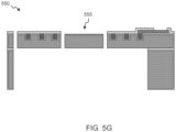
- FIGS. 5A-5G provide schematic illustrations of various points in the fabrication process for making a scanning micromirror device.
- the fabrication process begins with a silicon-on-insulator (SOI) wafer 500 as shown in FIG. 5A .
- SOI silicon-on-insulator
- the position of a conducting coil is established using a photolithography process, which can indicate positions of the SOI wafer 500 where the conducting coil will be embedded in a platform of the resultant scanning micromirror device.
- the silicon may be etched after the photolithography step to create recessed positions for the conducting coil, followed by stripping of any photoresist.
- the wafer may be subjected to a dry oxidation process, followed by deposition of a silicon nitride layer (SiN), such as using a low-pressure chemical vapor deposition method, to create an insulator separating the conducting coil from the silicon wafer.
- a metal seed layer 510 can be deposited into recesses, such as a tantalum/copper seed layer, by a sputtering process, for example.
- the wafer can appear similar to that shown in FIG. 5A , where the SOI wafer is identified by reference numeral 500, the recesses are identified by reference numeral 505, and the metal seed layer is identified by reference numeral 510.
- a copper layer can be deposited on the metal seed layer for bulk of the conducting coil, such as using an electrochemical deposition process.
- a chemical-mechanical polishing or planarization process can be used to remove excess copper and metal seed layer and create a flat surface of the device, resulting in the recesses being filled with copper.
- the wafer can appear similar to that shown in FIG. 5B , where the copper filled recesses are identified by reference numeral 515.
- a plasma-enhanced chemical vapor deposition process can be used to passivate the surface to create a silicon nitride/silicon oxide layer.
- a via 520 providing an access point for electrical contact to the conducting coil can be established by a photolithography process, followed by etching of the via and stripping of any remaining photoresist. At this point, the wafer can appear similar to that shown in FIG. 5C , where the via is identified by reference numeral 520.
- a second metal layer 525 can be deposited, such as a titanium/molybdenum layer.
- the second metal layer can provide an electrical connection to the conductive coil at the via 520 established above.
- the second metal layer 525 can be subjected to photolithography to define where the second metal layer 525 is to be retained, followed by an etching process (e.g., a wet etching process) and a photoresist stripping process.
- Another passivation layer 530 e.g., silicon oxide
- the wafer can appear similar to that shown in FIG. 5D , where the second metal layer is identified by reference numeral 525 and the passivation layer is identified by reference numeral 530.
- a photolithography process can be used to define the position of the platform of the scanning micromirror device and the top passivation layer can be thinned or removed by an etching process and any remaining photoresist can be stripped.
- a reflective layer 535 such as an aluminum layer can be deposited and patterned using a series of deposition, photolithography, etching and photoresist stripping processes.
- a passivation layer 530 may again be created (e.g., by plasma-enhanced chemical vapor deposition). At this point, the wafer can appear similar to that shown in FIG. 5E , where the reflector is identified by reference numeral 535 and the passivation layer is identified by reference numeral 540.
- a photolithography process can be used to define a second via 540 for connecting to the second metal layer, such as to allow wire bonding.
- the via can be etched followed by stripping any residual photoresist.
- Another photolithography process can be used to define regions between and surrounding the platform of the scanning micromirror device, the support flexures, and the frames (if any) positioned between the base and the platform.
- Recesses can be established by one or more etching processes, and a photoresist stripping process. At this point, the wafer can appear similar to that shown in FIG. 5F , where the via for the second metal layer is identified by reference numeral 545.
- a protective layer such as parylene
- the back side can be subjected to photolithography followed by one or more etching processes for removing silicon oxide layers, silicon nitride layers, the handle wafer and the buried oxide layers.
- the parylene and any residual photoresist layers can be stripped.
- the wafer can be diced, such as by a stealth or laser dicing process.
- the resultant wafer 550 can appear similar to that shown in FIG. 5G , where the scanning micromirror platform is identified by reference numeral 555.
- EXAMPLE 2 MANUFACTURING A SCANNING MICROMIRROR DEVICE A CONDUCTIVE COIL AND A STRESS-RELIEF LAYER
- This example provides an overview of a fabrication scheme for making a scanning micromirror device. Various details are described in this example that will allow the skilled artisan to understand example processes used for making scanning micromirror devices useful with the image projection systems, head-mounted display systems, and two-dimensional scanning systems described herein. It will be appreciated that conventional processes may be used for some fabrication steps. Not all fabrication steps may be described in detail in this example so as not to obscure other disclosed aspects. It will be appreciated that the figures described in this example are for illustrative purposes and may not be to scale.
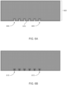
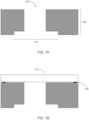
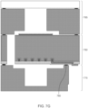
- FIGS. 6A-6H provide schematic illustrations of various points in the fabrication process for making a scanning micromirror device.
- the fabrication process begins with a silicon wafer 600, polished on both sides.
- the position of a conducting coil is established using a photolithography process, which can indicate positions of the wafer where the conducting coil will be embedded in a platform of the resultant scanning micromirror device.
- the silicon may be etched after the photolithography step to create recessed positions for the conducting coil, followed by stripping of any photoresist.
- the wafer may be subjected to a dry oxidation process, followed by deposition of a silicon nitride layer (SiN), such as using a low-pressure chemical vapor deposition method, to create an insulator separating the conducting coil from the silicon wafer.
- SiN silicon nitride layer
- a metal seed layer 610 can be deposited into recesses, such as a tantalum/copper seed layer, by a sputtering process, for example.
- the wafer can appear similar to that shown in FIG. 6A , where the silicon wafer is identified by reference numeral 600, the recesses are identified by reference numeral 605, and the metal seed layer is identified by reference numeral 610.
- a copper layer can be deposited on the metal seed layer for bulk of the conducting coil, such as using an electrochemical deposition process.
- a chemical-mechanical polishing or planarization process can be used to remove excess copper and metal seed layer and create a flat surface of the device, resulting in recesses 605 being filled with copper.
- the wafer can appear similar to that shown in FIG. 6B , where the copper filled recesses are identified by reference numeral 615.
- a plasma-enhanced chemical vapor deposition process can be used to passivate the surface to create a silicon nitride/silicon oxide layer.
- a via, providing an access point for electrical contact to the conducting coil can be established by a photolithography process, followed by etching of the via and stripping of any remaining photoresist. At this point, the wafer can appear similar to that shown in FIG. 6C , where the via is identified by reference numeral 620.
- a second metal layer 625 can be deposited, such as a titanium/molybdenum layer.
- the second metal layer can provide an electrical connection to the conductive coil at the via established above.
- the second metal layer 625 can be subjected to photolithography to define where the second metal layer 625 is to be retained, followed by an etching process (e.g., a wet etching process) and a photoresist stripping process.
- Another passivation layer 630 e.g., silicon oxide
- the wafer can appear similar to that shown in FIG. 6D , where the second metal layer is identified by reference numeral 625 and the passivation layer is identified by reference numeral 630.
- the above steps can all be used for creating a conducing coil on a back side of the silicon wafer.
- the reference terms back side and front side or top side and bottom side are merely examples describing relative opposite sides of a wafer and that these terms are not intended to be limiting.
- the steps outlined are merely one example of a process for making components of a scanning micromirror device and that other processes or orders of steps may be used.
- the overall shape of the scanning micromirror platform can be established from the front side of the device, by lithographically patterning and etching the passivation layers, followed etching the silicon through to the parylene layer, which is subsequently stripped.
- the wafer can be diced, such as by a stealth or laser dicing process, if desired.
- the resultant wafer 660 can have features similar to that shown in FIG. 6H . In some cases, the wafer can be diced later, such as after assembly of vacuum packaging, as described below in Example 3.
- the computing device also may comprise software elements, shown as being currently located within the working memory, including an operating system, device drivers, executable libraries, and/or other code, such as one or more application programs, which may comprise computer programs provided by various embodiments, and/or may be designed to implement methods, and/or configure systems, provided by other embodiments, as described herein.
- one or more procedures described with respect to the methods discussed above may be implemented as code and/or instructions executable by a computer (and/or a processor within a computer); in an aspect, then, such code and/or instructions may be used to configure and/or adapt a computer (or other device) to perform one or more operations in accordance with the described methods or for operation of the described devices and systems.
- machine-readable medium refers to any medium that participates in providing data that causes a machine to operate in a specific fashion. These mediums may be non-transitory.
- various computer-readable media may be involved in providing instructions/code to a processor for execution and/or may be used to store and/or carry such instructions/code.
- a computer-readable medium is a physical and/or tangible storage medium.
- Such a medium may take the form of a non-volatile media or volatile media.
- Non-volatile media include, for example, optical and/or magnetic disks, such as a non-transitory storage device.
- Volatile media include, without limitation, dynamic memory, such as the working memory.
- the communications subsystem (and/or components thereof) generally will receive signals, and the bus then may carry the signals (and/or the data, instructions, etc. carried by the signals) to the working memory, from which the processor retrieves and executes the instructions.
- the instructions received by the working memory may optionally be stored on a non-transitory storage device either before or after execution by the processor.
Landscapes
- Physics & Mathematics (AREA)
- General Physics & Mathematics (AREA)
- Optics & Photonics (AREA)
- Electromagnetism (AREA)
- Mechanical Optical Scanning Systems (AREA)
- Mechanical Light Control Or Optical Switches (AREA)
- Micromachines (AREA)
- Engineering & Computer Science (AREA)
- Mechanical Engineering (AREA)
- Computer Hardware Design (AREA)
- Microelectronics & Electronic Packaging (AREA)
Applications Claiming Priority (4)
| Application Number | Priority Date | Filing Date | Title |
|---|---|---|---|
| US202062962168P | 2020-01-16 | 2020-01-16 | |
| US202063058384P | 2020-07-29 | 2020-07-29 | |
| EP21741743.5A EP4091012B1 (de) | 2020-01-16 | 2021-01-15 | Abtastende spiegelsysteme und herstellungsverfahren |
| PCT/US2021/013676 WO2021146583A1 (en) | 2020-01-16 | 2021-01-15 | Scanning mirror systems and methods of manufacture |
Related Parent Applications (1)
| Application Number | Title | Priority Date | Filing Date |
|---|---|---|---|
| EP21741743.5A Division EP4091012B1 (de) | 2020-01-16 | 2021-01-15 | Abtastende spiegelsysteme und herstellungsverfahren |
Publications (2)
| Publication Number | Publication Date |
|---|---|
| EP4492125A2 true EP4492125A2 (de) | 2025-01-15 |
| EP4492125A3 EP4492125A3 (de) | 2025-04-09 |
Family
ID=76857628
Family Applications (2)
| Application Number | Title | Priority Date | Filing Date |
|---|---|---|---|
| EP24208450.7A Pending EP4492125A3 (de) | 2020-01-16 | 2021-01-15 | Abtastspiegelsysteme und herstellungsverfahren |
| EP21741743.5A Active EP4091012B1 (de) | 2020-01-16 | 2021-01-15 | Abtastende spiegelsysteme und herstellungsverfahren |
Family Applications After (1)
| Application Number | Title | Priority Date | Filing Date |
|---|---|---|---|
| EP21741743.5A Active EP4091012B1 (de) | 2020-01-16 | 2021-01-15 | Abtastende spiegelsysteme und herstellungsverfahren |
Country Status (5)
| Country | Link |
|---|---|
| US (2) | US11796791B2 (de) |
| EP (2) | EP4492125A3 (de) |
| JP (1) | JP7665631B2 (de) |
| CN (1) | CN114981704A (de) |
| WO (1) | WO2021146583A1 (de) |
Families Citing this family (7)
| Publication number | Priority date | Publication date | Assignee | Title |
|---|---|---|---|---|
| EP4492125A3 (de) | 2020-01-16 | 2025-04-09 | Magic Leap, Inc. | Abtastspiegelsysteme und herstellungsverfahren |
| JP7796649B2 (ja) | 2020-01-22 | 2026-01-09 | マジック リープ, インコーポレイテッド | 2つのミラー走査リレー光学系 |
| US12061333B2 (en) | 2020-06-04 | 2024-08-13 | Magic Leap, Inc. | Two-dimensional micro-electrical mechanical system mirror and actuation method |
| US20230067786A1 (en) * | 2021-08-31 | 2023-03-02 | Compertum Microsystems Inc. | Hermetically packaged scanning mirror in low humidity environment and manufacturing method thereof |
| CN115308897B (zh) * | 2022-08-26 | 2024-09-24 | 觉芯电子(无锡)有限公司 | 一种具有线圈堆叠结构的电磁驱动微镜及生产工艺 |
| CN115308899B (zh) * | 2022-08-29 | 2024-09-24 | 觉芯电子(无锡)有限公司 | 一种带有高密度线圈的电磁驱动微镜装置及制备工艺 |
| CN116300054A (zh) * | 2023-04-06 | 2023-06-23 | 中科融合感知智能研究院(苏州工业园区)有限公司 | 一种集成温度传感器的一维电磁扫描微镜 |
Citations (2)
| Publication number | Priority date | Publication date | Assignee | Title |
|---|---|---|---|---|
| US6856446B2 (en) | 2001-12-12 | 2005-02-15 | Texas Instruments Incorporated | Digital micromirror device having mirror-attached spring tips |
| EP4091012A1 (de) | 2020-01-16 | 2022-11-23 | Magic Leap, Inc. | Abtastende spiegelsysteme und herstellungsverfahren |
Family Cites Families (48)
| Publication number | Priority date | Publication date | Assignee | Title |
|---|---|---|---|---|
| US2771813A (en) | 1952-09-05 | 1956-11-27 | Eastman Kodak Co | Apparatus for continuous motion picture projection |
| US3748015A (en) | 1971-06-21 | 1973-07-24 | Perkin Elmer Corp | Unit power imaging catoptric anastigmat |
| WO1982003924A1 (en) | 1981-05-07 | 1982-11-11 | Stig Leopold Berglund | Afocal apparatus for the optical-mechanical scanning of an object |
| SE512336C2 (sv) | 1998-06-09 | 2000-02-28 | Celsiustech Electronics Ab | Anordning vid optomekanisk, bärbar deflektor för displayenhet |
| AU2001286745A1 (en) * | 2000-08-27 | 2002-03-13 | Corning Intellisense Corporation | Magnetically actuated micro-electro-mechanical apparatus and method of manufacture |
| US6323984B1 (en) | 2000-10-11 | 2001-11-27 | Silicon Light Machines | Method and apparatus for reducing laser speckle |
| US6956274B2 (en) * | 2002-01-11 | 2005-10-18 | Analog Devices, Inc. | TiW platinum interconnect and method of making the same |
| JP4082075B2 (ja) | 2002-04-22 | 2008-04-30 | ブラザー工業株式会社 | 画像表示装置 |
| US7071594B1 (en) | 2002-11-04 | 2006-07-04 | Microvision, Inc. | MEMS scanner with dual magnetic and capacitive drive |
| US7442918B2 (en) | 2004-05-14 | 2008-10-28 | Microvision, Inc. | MEMS device having simplified drive |
| EP1635209A3 (de) | 2004-09-13 | 2006-04-05 | Canon Kabushiki Kaisha | Abbildendes optisches System und Bilderfassungsgerät ausgerüstet mit demselben |
| WO2006035378A1 (en) | 2004-09-28 | 2006-04-06 | Koninklijke Philips Electronics N.V. | Two dimensional micro scanner |
| JP4921366B2 (ja) | 2005-04-15 | 2012-04-25 | パナソニック株式会社 | 微小機械構造体システムおよびその製造方法 |
| KR100743315B1 (ko) * | 2005-08-26 | 2007-07-26 | 엘지전자 주식회사 | 마이크로 미러 디바이스 및 이를 이용한 마이크로 미러디바이스 어레이 |
| JP2007178942A (ja) | 2005-12-28 | 2007-07-12 | Brother Ind Ltd | 光走査装置、画像表示装置及び網膜走査型画像表示装置 |
| US7545446B2 (en) | 2005-08-27 | 2009-06-09 | Hewlett-Packard Development Company, L.P. | Offner relay for projection system |
| US7261430B1 (en) * | 2006-02-22 | 2007-08-28 | Teledyne Licensing, Llc | Thermal and intrinsic stress compensated micromirror apparatus and method |
| US7834867B2 (en) * | 2006-04-11 | 2010-11-16 | Microvision, Inc. | Integrated photonics module and devices using integrated photonics modules |
| KR100738114B1 (ko) * | 2006-05-18 | 2007-07-12 | 삼성전자주식회사 | 액츄에이터 및 이차원 스캐너 |
| US20080078363A1 (en) * | 2006-09-28 | 2008-04-03 | John D. Sims | Fuel vaporization system and method |
| JP2009093105A (ja) * | 2007-10-12 | 2009-04-30 | Hoya Corp | マイクロミラー装置、およびミラー部形成方法 |
| JP2009251143A (ja) * | 2008-04-03 | 2009-10-29 | Seiko Epson Corp | アクチュエータ、画像形成装置及びアクチュエータの製造方法 |
| US7986449B2 (en) | 2008-05-16 | 2011-07-26 | Microvision, Inc. | Induced resonance comb drive scanner |
| US8373690B2 (en) | 2008-10-17 | 2013-02-12 | Panasonic Corporation | Scanning image display apparatus |
| US8274720B2 (en) | 2009-02-15 | 2012-09-25 | Kessler Optics and Photonics Solutions, Ltd. | Concentric afocal beam relay |
| US8531750B2 (en) | 2009-02-15 | 2013-09-10 | Kessler Optics & Photonics Solutions, Ltd. | Afocal beam relay |
| US8817379B2 (en) | 2011-07-12 | 2014-08-26 | Google Inc. | Whole image scanning mirror display system |
| GB201222370D0 (en) | 2012-01-24 | 2013-01-23 | Grahmann Jan | Scanning device |
| JP6369906B2 (ja) | 2012-03-09 | 2018-08-08 | カール・ツァイス・エスエムティー・ゲーエムベーハー | Euv投影リソグラフィのための照明光学ユニット及びそのような照明光学ユニットを含む光学系 |
| JP6024332B2 (ja) * | 2012-09-19 | 2016-11-16 | 船井電機株式会社 | 画像表示装置 |
| EP2906985B1 (de) | 2012-10-12 | 2022-03-09 | Thorlabs, Inc. | Kompaktes, adaptives optisches abtastsystem mit geringer dispersion und abberration |
| JP2014119616A (ja) * | 2012-12-17 | 2014-06-30 | Canon Electronics Inc | マイクロデバイス及び光偏向器並びに光学デバイス |
| US9063549B1 (en) * | 2013-03-06 | 2015-06-23 | Google Inc. | Light detection and ranging device with oscillating mirror driven by magnetically interactive coil |
| US9335544B2 (en) * | 2013-03-15 | 2016-05-10 | Rit Wireless Ltd. | Electrostatically steerable actuator |
| JP5916667B2 (ja) * | 2013-07-17 | 2016-05-11 | 富士フイルム株式会社 | ミラー駆動装置及びその駆動方法 |
| US20160187643A1 (en) | 2014-12-31 | 2016-06-30 | Lexmark International Inc. | Micro-Electromechanical System (MEMS) Devices and Methods for Packaging the Same |
| US9910270B2 (en) * | 2015-10-12 | 2018-03-06 | Intel Corporation | Electro-mechanical designs for MEMS scanning mirrors |
| TWI638419B (zh) * | 2016-04-18 | 2018-10-11 | 村田製作所股份有限公司 | 一種掃描鏡設備與其製造方法 |
| JP2018060029A (ja) * | 2016-10-04 | 2018-04-12 | 矢崎総業株式会社 | ミラー装置および車両用表示装置 |
| JP6875118B2 (ja) * | 2016-12-20 | 2021-05-19 | 株式会社日立エルジーデータストレージ | レーザ投射表示装置 |
| US10114215B1 (en) | 2017-04-17 | 2018-10-30 | Microvision, Inc. | Scanning laser devices with reduced exit pupil disparity |
| CN115657297A (zh) * | 2017-11-15 | 2023-01-31 | 浜松光子学株式会社 | 光学器件的制造方法 |
| US10921580B2 (en) | 2018-03-07 | 2021-02-16 | Microsoft Technology Licensing, Llc | Systems and methods of increasing pupil size in a display system |
| US10935640B2 (en) * | 2018-04-25 | 2021-03-02 | Microvision, Inc. | Multiplexed LIDAR transceiver |
| DE102018209886B4 (de) | 2018-06-19 | 2020-02-27 | Fraunhofer-Gesellschaft zur Förderung der angewandten Forschung e.V. | Einrichtung zur Projektion eines Laserstrahls zur Erzeugung eines Bildes auf der Netzhaut eines Auges und Brilleneinrichtung mit zwei derartigen Einrichtungen |
| CN110806639B (zh) | 2019-12-19 | 2025-02-11 | 成都英飞睿技术有限公司 | 一种微型投影扫描系统 |
| JP7796649B2 (ja) | 2020-01-22 | 2026-01-09 | マジック リープ, インコーポレイテッド | 2つのミラー走査リレー光学系 |
| US12061333B2 (en) | 2020-06-04 | 2024-08-13 | Magic Leap, Inc. | Two-dimensional micro-electrical mechanical system mirror and actuation method |
-
2021
- 2021-01-15 EP EP24208450.7A patent/EP4492125A3/de active Pending
- 2021-01-15 WO PCT/US2021/013676 patent/WO2021146583A1/en not_active Ceased
- 2021-01-15 US US17/150,694 patent/US11796791B2/en active Active
- 2021-01-15 JP JP2022542944A patent/JP7665631B2/ja active Active
- 2021-01-15 CN CN202180010024.3A patent/CN114981704A/zh active Pending
- 2021-01-15 EP EP21741743.5A patent/EP4091012B1/de active Active
-
2023
- 2023-09-19 US US18/370,009 patent/US12601906B2/en active Active
Patent Citations (2)
| Publication number | Priority date | Publication date | Assignee | Title |
|---|---|---|---|---|
| US6856446B2 (en) | 2001-12-12 | 2005-02-15 | Texas Instruments Incorporated | Digital micromirror device having mirror-attached spring tips |
| EP4091012A1 (de) | 2020-01-16 | 2022-11-23 | Magic Leap, Inc. | Abtastende spiegelsysteme und herstellungsverfahren |
Also Published As
| Publication number | Publication date |
|---|---|
| US20210223541A1 (en) | 2021-07-22 |
| WO2021146583A1 (en) | 2021-07-22 |
| US12601906B2 (en) | 2026-04-14 |
| US20240012237A1 (en) | 2024-01-11 |
| US11796791B2 (en) | 2023-10-24 |
| CN114981704A (zh) | 2022-08-30 |
| JP2023511539A (ja) | 2023-03-20 |
| EP4091012B1 (de) | 2024-10-30 |
| JP7665631B2 (ja) | 2025-04-21 |
| EP4492125A3 (de) | 2025-04-09 |
| EP4091012A1 (de) | 2022-11-23 |
| EP4091012A4 (de) | 2023-07-26 |
Similar Documents
| Publication | Publication Date | Title |
|---|---|---|
| US12601906B2 (en) | Scanning mirror systems and methods of manufacture | |
| JP7363177B2 (ja) | 光偏向器、光走査システム、画像投影装置、画像形成装置、レーザレーダ | |
| JP7243174B2 (ja) | 可動装置、距離測定装置、画像投影装置、及び車両 | |
| US11624903B2 (en) | Light deflector, LiDAR device, and image forming apparatus | |
| JP2023174680A (ja) | 可動装置、画像投影装置、ヘッドアップディスプレイ、レーザヘッドランプ、ヘッドマウントディスプレイ、物体認識装置、及び車両 | |
| EP4045962B1 (de) | Bewegbare vorrichtung | |
| EP3473004B1 (de) | Steuerungsvorrichtung, bildprojektionsvorrichtung und steuerungsverfahren | |
| JP7363352B2 (ja) | 可動装置、画像投影装置、ヘッドアップディスプレイ、レーザヘッドランプ、ヘッドマウントディスプレイ、物体認識装置、及び車両 | |
| JP5070869B2 (ja) | 光走査装置及びそれを備えた網膜走査型画像表示装置 | |
| CA3123184C (en) | Movable device, distance measurement device, image projection apparatus, vehicle, and mount | |
| JP2017116842A (ja) | 光偏向器及び画像投影装置 | |
| JP6926625B2 (ja) | 圧電アクチュエータ、光偏向器及び画像投影装置 | |
| JP7639424B2 (ja) | 可動装置、画像投影装置、ヘッドアップディスプレイ、レーザヘッドランプ、ヘッドマウントディスプレイ、距離測定装置、及び移動体 | |
| JP6834227B2 (ja) | 光偏向器、画像表示装置、画像投影装置、光書き込み装置、物体認識装置、車両 | |
| JP2017016018A (ja) | 光偏向器、光走査装置、画像形成装置、画像投影装置、ヘッドアップディスプレイ装置、およびレーダ装置 | |
| JP5557113B2 (ja) | 画像表示装置 | |
| CN115768716A (zh) | 具有邻近于扫描镜的相对侧而悬臂的致动器对的微机电系统(mems)扫描仪 | |
| JP2006189790A (ja) | オープンホールを基盤とする回折光変調器 | |
| JP2006201783A (ja) | 電磁力駆動スキャニングマイクロミラー及びこれを使用した光スキャニング装置 | |
| JP2008116932A (ja) | 映像歪み補正方法及びその装置 | |
| US20240288683A1 (en) | Microscanner having meander spring-based mirror suspension | |
| Hoskinson et al. | Arrays of large-area, tip/tilt micromirrors for use in a high-contrast projector | |
| JP2007310386A (ja) | 光変調器キャリブレーション装置 | |
| WO2017221792A1 (en) | Control device, image projection apparatus, and control method | |
| JP2018013546A (ja) | 光偏向器、光走査装置、画像投影装置および画像形成装置 |
Legal Events
| Date | Code | Title | Description |
|---|---|---|---|
| PUAI | Public reference made under article 153(3) epc to a published international application that has entered the european phase |
Free format text: ORIGINAL CODE: 0009012 |
|
| STAA | Information on the status of an ep patent application or granted ep patent |
Free format text: STATUS: THE APPLICATION HAS BEEN PUBLISHED |
|
| AC | Divisional application: reference to earlier application |
Ref document number: 4091012 Country of ref document: EP Kind code of ref document: P |
|
| AK | Designated contracting states |
Kind code of ref document: A2 Designated state(s): AL AT BE BG CH CY CZ DE DK EE ES FI FR GB GR HR HU IE IS IT LI LT LU LV MC MK MT NL NO PL PT RO RS SE SI SK SM TR |
|
| REG | Reference to a national code |
Ref country code: DE Ref legal event code: R079 Free format text: PREVIOUS MAIN CLASS: G02B0027010000 Ipc: G02B0026100000 |
|
| PUAL | Search report despatched |
Free format text: ORIGINAL CODE: 0009013 |
|
| AK | Designated contracting states |
Kind code of ref document: A3 Designated state(s): AL AT BE BG CH CY CZ DE DK EE ES FI FR GB GR HR HU IE IS IT LI LT LU LV MC MK MT NL NO PL PT RO RS SE SI SK SM TR |
|
| RIC1 | Information provided on ipc code assigned before grant |
Ipc: G02B 26/08 20060101ALI20250306BHEP Ipc: G02B 26/10 20060101AFI20250306BHEP |
|
| STAA | Information on the status of an ep patent application or granted ep patent |
Free format text: STATUS: REQUEST FOR EXAMINATION WAS MADE |
|
| 17P | Request for examination filed |
Effective date: 20251008 |
|
| GRAP | Despatch of communication of intention to grant a patent |
Free format text: ORIGINAL CODE: EPIDOSNIGR1 |
|
| STAA | Information on the status of an ep patent application or granted ep patent |
Free format text: STATUS: GRANT OF PATENT IS INTENDED |
|
| RIC1 | Information provided on ipc code assigned before grant |
Ipc: G02B 26/10 20060101AFI20260211BHEP Ipc: G02B 26/08 20060101ALI20260211BHEP |
|
| INTG | Intention to grant announced |
Effective date: 20260225 |
|
| GRAS | Grant fee paid |
Free format text: ORIGINAL CODE: EPIDOSNIGR3 |