EP4472077A2 - Zeit-digital-wandler und verfahren zum messen der zeit zwischen taktflanken - Google Patents
Zeit-digital-wandler und verfahren zum messen der zeit zwischen taktflanken Download PDFInfo
- Publication number
- EP4472077A2 EP4472077A2 EP24188710.8A EP24188710A EP4472077A2 EP 4472077 A2 EP4472077 A2 EP 4472077A2 EP 24188710 A EP24188710 A EP 24188710A EP 4472077 A2 EP4472077 A2 EP 4472077A2
- Authority
- EP
- European Patent Office
- Prior art keywords
- oscillator
- clock
- time
- output signal
- slow
- Prior art date
- Legal status (The legal status is an assumption and is not a legal conclusion. Google has not performed a legal analysis and makes no representation as to the accuracy of the status listed.)
- Pending
Links
- 238000000034 method Methods 0.000 title claims description 18
- 238000005259 measurement Methods 0.000 claims description 75
- 238000001514 detection method Methods 0.000 claims description 5
- 239000003990 capacitor Substances 0.000 claims description 2
- 230000001934 delay Effects 0.000 claims description 2
- 230000000630 rising effect Effects 0.000 description 19
- 238000010586 diagram Methods 0.000 description 10
- 238000012216 screening Methods 0.000 description 8
- 230000003071 parasitic effect Effects 0.000 description 5
- 230000010355 oscillation Effects 0.000 description 4
- 230000008569 process Effects 0.000 description 4
- 101100328957 Caenorhabditis elegans clk-1 gene Proteins 0.000 description 3
- 230000004044 response Effects 0.000 description 3
- 230000009897 systematic effect Effects 0.000 description 3
- 238000012360 testing method Methods 0.000 description 3
- 101100113692 Caenorhabditis elegans clk-2 gene Proteins 0.000 description 2
- 238000012986 modification Methods 0.000 description 2
- 230000004048 modification Effects 0.000 description 2
- 230000001960 triggered effect Effects 0.000 description 2
- 238000013459 approach Methods 0.000 description 1
- 239000013078 crystal Substances 0.000 description 1
- 230000003111 delayed effect Effects 0.000 description 1
- 230000003993 interaction Effects 0.000 description 1
- 239000000463 material Substances 0.000 description 1
- 238000012544 monitoring process Methods 0.000 description 1
- 238000012805 post-processing Methods 0.000 description 1
- 238000012545 processing Methods 0.000 description 1
- 230000009467 reduction Effects 0.000 description 1
- 238000007493 shaping process Methods 0.000 description 1
- 238000006467 substitution reaction Methods 0.000 description 1
Images


Classifications
-
- G—PHYSICS
- G04—HOROLOGY
- G04F—TIME-INTERVAL MEASURING
- G04F10/00—Apparatus for measuring unknown time intervals by electric means
- G04F10/005—Time-to-digital converters [TDC]
-
- G—PHYSICS
- G04—HOROLOGY
- G04F—TIME-INTERVAL MEASURING
- G04F10/00—Apparatus for measuring unknown time intervals by electric means
- G04F10/04—Apparatus for measuring unknown time intervals by electric means by counting pulses or half-cycles of an AC
-
- H—ELECTRICITY
- H03—ELECTRONIC CIRCUITRY
- H03K—PULSE TECHNIQUE
- H03K3/00—Circuits for generating electric pulses; Monostable, bistable or multistable circuits
- H03K3/01—Details
- H03K3/011—Modifications of generator to compensate for variations in physical values, e.g. voltage, temperature
-
- H—ELECTRICITY
- H03—ELECTRONIC CIRCUITRY
- H03K—PULSE TECHNIQUE
- H03K3/00—Circuits for generating electric pulses; Monostable, bistable or multistable circuits
- H03K3/02—Generators characterised by the type of circuit or by the means used for producing pulses
- H03K3/027—Generators characterised by the type of circuit or by the means used for producing pulses by the use of logic circuits, with internal or external positive feedback
- H03K3/03—Astable circuits
- H03K3/0315—Ring oscillators
-
- H—ELECTRICITY
- H03—ELECTRONIC CIRCUITRY
- H03K—PULSE TECHNIQUE
- H03K5/00—Manipulating of pulses not covered by one of the other main groups of this subclass
- H03K5/22—Circuits having more than one input and one output for comparing pulses or pulse trains with each other according to input signal characteristics, e.g. slope, integral
- H03K5/26—Circuits having more than one input and one output for comparing pulses or pulse trains with each other according to input signal characteristics, e.g. slope, integral the characteristic being duration, interval, position, frequency, or sequence
-
- H—ELECTRICITY
- H03—ELECTRONIC CIRCUITRY
- H03L—AUTOMATIC CONTROL, STARTING, SYNCHRONISATION OR STABILISATION OF GENERATORS OF ELECTRONIC OSCILLATIONS OR PULSES
- H03L7/00—Automatic control of frequency or phase; Synchronisation
- H03L7/06—Automatic control of frequency or phase; Synchronisation using a reference signal applied to a frequency- or phase-locked loop
- H03L7/08—Details of the phase-locked loop
- H03L7/099—Details of the phase-locked loop concerning mainly the controlled oscillator of the loop
- H03L7/0995—Details of the phase-locked loop concerning mainly the controlled oscillator of the loop the oscillator comprising a ring oscillator
- H03L7/0996—Selecting a signal among the plurality of phase-shifted signals produced by the ring oscillator
-
- H—ELECTRICITY
- H03—ELECTRONIC CIRCUITRY
- H03L—AUTOMATIC CONTROL, STARTING, SYNCHRONISATION OR STABILISATION OF GENERATORS OF ELECTRONIC OSCILLATIONS OR PULSES
- H03L7/00—Automatic control of frequency or phase; Synchronisation
- H03L7/06—Automatic control of frequency or phase; Synchronisation using a reference signal applied to a frequency- or phase-locked loop
- H03L7/08—Details of the phase-locked loop
- H03L7/14—Details of the phase-locked loop for assuring constant frequency when supply or correction voltages fail
- H03L7/141—Details of the phase-locked loop for assuring constant frequency when supply or correction voltages fail the phase-locked loop controlling several oscillators in turn
-
- H—ELECTRICITY
- H03—ELECTRONIC CIRCUITRY
- H03L—AUTOMATIC CONTROL, STARTING, SYNCHRONISATION OR STABILISATION OF GENERATORS OF ELECTRONIC OSCILLATIONS OR PULSES
- H03L7/00—Automatic control of frequency or phase; Synchronisation
- H03L7/06—Automatic control of frequency or phase; Synchronisation using a reference signal applied to a frequency- or phase-locked loop
- H03L7/16—Indirect frequency synthesis, i.e. generating a desired one of a number of predetermined frequencies using a frequency- or phase-locked loop
- H03L7/18—Indirect frequency synthesis, i.e. generating a desired one of a number of predetermined frequencies using a frequency- or phase-locked loop using a frequency divider or counter in the loop
- H03L7/183—Indirect frequency synthesis, i.e. generating a desired one of a number of predetermined frequencies using a frequency- or phase-locked loop using a frequency divider or counter in the loop a time difference being used for locking the loop, the counter counting between fixed numbers or the frequency divider dividing by a fixed number
- H03L7/187—Indirect frequency synthesis, i.e. generating a desired one of a number of predetermined frequencies using a frequency- or phase-locked loop using a frequency divider or counter in the loop a time difference being used for locking the loop, the counter counting between fixed numbers or the frequency divider dividing by a fixed number using means for coarse tuning the voltage controlled oscillator of the loop
-
- H—ELECTRICITY
- H03—ELECTRONIC CIRCUITRY
- H03L—AUTOMATIC CONTROL, STARTING, SYNCHRONISATION OR STABILISATION OF GENERATORS OF ELECTRONIC OSCILLATIONS OR PULSES
- H03L7/00—Automatic control of frequency or phase; Synchronisation
- H03L7/06—Automatic control of frequency or phase; Synchronisation using a reference signal applied to a frequency- or phase-locked loop
- H03L7/16—Indirect frequency synthesis, i.e. generating a desired one of a number of predetermined frequencies using a frequency- or phase-locked loop
- H03L7/18—Indirect frequency synthesis, i.e. generating a desired one of a number of predetermined frequencies using a frequency- or phase-locked loop using a frequency divider or counter in the loop
- H03L7/183—Indirect frequency synthesis, i.e. generating a desired one of a number of predetermined frequencies using a frequency- or phase-locked loop using a frequency divider or counter in the loop a time difference being used for locking the loop, the counter counting between fixed numbers or the frequency divider dividing by a fixed number
- H03L7/191—Indirect frequency synthesis, i.e. generating a desired one of a number of predetermined frequencies using a frequency- or phase-locked loop using a frequency divider or counter in the loop a time difference being used for locking the loop, the counter counting between fixed numbers or the frequency divider dividing by a fixed number using at least two different signals from the frequency divider or the counter for determining the time difference
Definitions
- This application relates to clock measurement, and more particularly to a sub-ranging time-to-digital clock measurement.
- Modem devices such as smartphones and tablets demand stringent clock performance standards for its various sub-systems such as digital cores, data converters, and frequency synthesizers.
- clock performance for digital cores must satisfy low period jitter and low duty-cycle error.
- data converters require clock signals with low absolute jitter (time internal error (TIE)).
- frequency synthesizers require clock signals with low phase noise and reduced fractional spurs. Emerging self-driving automotive application also demand stringent clock performance.
- a clock screening circuit that includes a time-to-digital converter that is insensitive to process variations and also includes a clock interface that supports multiple modes for screening various clock performance metrics.
- a subranging time-to-digital converter that measures the time difference between a first clock edge for a clock signal and a second edge using a fine count and a coarse count.
- the TDC includes a slow oscillator that begins oscillating a slow oscillator output signal responsive to first clock edge.
- a coarse counter counts the coarse count responsive to the slow oscillator output signal.
- the TDC also includes a fast oscillator that begins oscillating a fast oscillator output signal responsive to a second clock edge, which may arrive either later or earlier than the first clock edge.
- a fine counter counts the fine count responsive to the fast oscillator output signal.
- the TDC may be integrated into a clock measurement circuit that enables a wide variety of clock measurements such as period jitter measurement, K-cycle jitter measurement, duty cycle measurement, time internal error (TIE) measurement, and clock skew measurement.
- clock measurements such as period jitter measurement, K-cycle jitter measurement, duty cycle measurement, time internal error (TIE) measurement, and clock skew measurement.
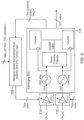
- Clock measurement circuit 100 (which may also be denoted as a built-in-self-test (BIST) circuit) is shown in Figure 1 .
- Clock measurement circuit 100 includes a clock interface 105 that supports multiple clock screening modes of operation such as period jitter measurement, K-cycle jitter measurement, duty cycle measurement, clock skew, and time internal error (TIE) measurement.
- Clock interface 105 is quite advantageous in that the conventional need for multiple clock measurement circuits to service such diverse clock testing modes is obviated.
- clock interface 105 will select two clock edges from one or more input clock signals.
- clock interface 105 may select for a phase-locked loop (PLL) clock signal to perform the period jitter measurement, the duty cycle measurement, and the K-cycle jitter measurement as will be explained further herein.
- PLL phase-locked loop
- DLL delay-locked loop
- clock interface 105 selects for a first clock edge of a clock signal such as received from a clock-tree output node and also for a second clock edge of another clock signal such as received from another clock-tree output node. Either the first clock edge or the second clock edge may be earlier than the remaining one of the first and second clock edges.
- clock interface 105 selects for an edge of a clock signal such as the PLL clock signal and also for an edge of a reference clock signal (Ref CLK) such as a crystal oscillator signal.
- a clock signal such as the PLL clock signal
- Ref CLK reference clock signal
- TDC 110 is formed using a subranging architecture that includes a pair of ring oscillators (not shown in Figure 1 ) that each include as few as three inverters. TDC 110 thus is compact yet achieves high resolution across a wide input range of frequencies.
- a controller 115 controls clock interface 105 and TDC 110 as well as their interaction.
- the output of TDC 110 is a digital number corresponding to the measurement of the delay between the two clock edges.
- TDC 110 is shown in more detail in Figure 2A .
- clock interface 105 of Figure 1 has selected two clock edges from its received clock signals depending upon the desired clock measurement.
- the type of clock edge also depends upon the desired clock measurement. For example, a period jitter measurement or a K-cycle jitter measurement may involve the selection of two rising clock edges such as shown in Figure 2A .
- two falling clock edges may be selected for such measurements.
- the selected clock signal edge that is leading the remaining selected clock edge is denoted in Figure 2A as the CLK early signal whereas the lagging selected clock signal edge is denoted as CLK late.
- the rising edge for the CLK early signal triggers a slow oscillator 205 to begin oscillating such as in response to the assertion of an enable signal En1 at the time of the rising edge.
- slow oscillator 205 oscillates more slowly as compared to a fast oscillator 210 that is triggered to oscillate by the rising edge of the CLK late signal such as through the corresponding assertion of an enable signal En2.
- ⁇ t delay between the CLK early and CLK late edges
- slow oscillator 205 will oscillate a slow oscillator output signal a certain number of oscillation periods prior to the triggering of fast oscillator 210 to oscillate its fast oscillator output signal.
- the slow oscillator output signal clocks a coarse counter 220 to begin counting cycles of the slow oscillator output signal whereas the fast oscillator output signal clocks a fine counter 225 to begin counting cycles of the fast oscillator output signal.
- a first cycle of the fast oscillator output signal will typically be lagging in phase as compared to the slow oscillator output signal from slow oscillator 205. It will then take a certain number of oscillation periods for the fast oscillator output signal before the slow oscillator output signal is lagging the fast oscillator output signal.
- Phase detector 215 detects when the fast oscillator output signal catches up in phase and begins leading the slow oscillator output signal and triggers coarse counter 220 and fine counter 225 to latch their count.
- the latched count for fine counter 225 may be designated as Nfine.
- FIG. 2B An example timing diagram for the slow oscillator output signal (designated as OSC slow) and for the fast oscillator output signal (designated as OSC fast) is shown in Figure 2B .
- the delay ⁇ t between the CLK early and CLK late signals ( Figure 2A ) equals a sum of a coarse delay ( ⁇ tcoarse) and a fine delay ( ⁇ tfine).
- Tslow the period for the slow oscillator output signal
- Tfast the period for the fast oscillator output signal
- the slow oscillator output signal oscillates through two Tslow periods plus a fraction of another Tslow period before the rising edge of the fast oscillator output signal.
- the total delay ⁇ t equals the two Tslow periods plus this additional fraction of the Tslow period.
- a coarse count Ncoarse equals the integer number of Tslow periods between the CLK early and CLK late edges. It can thus be shown that the delay ⁇ t equals the Ncoarse*Tslow + Nfine * (Tslow - Tfast).
- coarse counter 220 may be latched responsive to the CLK late edge in alternative implementations. In such an implementation, Ncoarse would equal the count latched by coarse counter 220.
- TDC 110 may adjust the count latched by coarse counter 220 accordingly to obtain Ncoarse. If the delay ⁇ t processed by TDC 110 is negative, fast oscillator 210 will start earlier than slow oscillator 205. The counts from coarse counter 220 and fine counter 225 can then be collected in similar way as shown in Figure 2B to resolve a negative time-difference value with respect to TDC input ⁇ t. Using the counter latch method of Figure 2B , the sign of a difference between counter 220 and counter 225 after latching indicates the polarity of input ⁇ t.
- a desired ratio between Tslow and Tfast may be calibrated by controller 115 prior to the clock measurements such as through comparison to the reference clock signal. For example, controller 115 may count the number of oscillation cycles for slow oscillator 205 and fast oscillator 210 in one or more reference clock cycles. Controller 115 would then adjust a frequency tune word for slow oscillator 205 and/or a frequency tune word for fast oscillator 210 to enforce the desired relationship between Tslow and Tfast as well as their absolute values.
- the time measurement by TDC 110 should be robust to voltage variations for its power supply voltage.
- the variations from chip power supply or from current drawn by slow oscillator 205 and fast oscillator 210 may cause the power supply voltage for TDC 110 to fluctuate, which affects the accuracy of the desired clock measurement.
- a robust power supply scheme for TDC 110 is shown in Figure 3 .
- An oscillator power domain 315 powers slow oscillator 205 and fast oscillator 210 based upon an oscillator power supply voltage Vreg_out from a linear regulator 305 as isolated from the chip power supply and smoothed through a decoupling capacitor Cdecap.
- Linear regulator 305 converts its own regulator power supply voltage Vdd_IP to supply and regulate oscillator power supply voltage Vreg_out.
- oscillator power domain 315 includes dummy current source loads 320 and 315.
- Dummy current source load 320 is configured to draw the same current as drawn by slow oscillator 205.
- slow oscillator 205 may include as few as three inverters 330 arranged to form a ring oscillator. This is quite advantageous as compared to the typically much larger number of delay circuits required by conventional TDC designs.
- fast oscillator 210 is formed using three inverters 335 arranged to form a ring oscillator.
- Dummy current source load 325 is configured to draw the same current as drawn by fast oscillator 210.
- TDC 110 measures the time delay ⁇ t between two clock edges.
- the two clock edges are denoted as Clk1 and Clk2 in Figure 3 .
- Clk1 and Clk2 are denoted in Figure 3 as directly driving their corresponding oscillator (fast or slow) without the intermediary enabling signals En1 and En2 discussed with regard to Figure 2 .
- the rising edge for the Clk1 signal causes slow oscillator 205 to begin oscillating and drawing its operating current.
- dummy current source load 320 sinks a replica of this operating current.
- Dummy current source load 320 is configured to stop sinking this replica operating current in response to the rising edge of the Clk1 signal.
- slow oscillator 205 will thus not perturb the oscillator power supply voltage as the there is no sudden current demand caused by the triggering of slow oscillator 205.
- dummy current source load 235 sinks a replica of an operating current that will be drawn by fast oscillator 210 and is configured to stop sinking this replica operating current responsive to the rising edge for the Clk2 signal.
- the triggering of fast oscillator 210 will thus also not cause a sudden current demand that could perturb the oscillator power supply voltage Vreg_out.
- the clock measurements described herein may be robust to power supply voltage variations such as caused by package and chip parasitics 310.
- Clock interface 105 is shown in more detail in Figure 4A .
- a down counter 405 responds to an enable signal by updating a Q signal bus (typically a counter signal represented in binary) as clocked by a selected clock signal.
- clock interface 105 may select from a plurality of clock signals depending upon the clock measurement mode.
- clock interface 105 may include a clock multiplexer (not illustrated) that selects for the appropriate clock signal to clock the flip-flops in down counter 405.
- clock edges K cycles apart are tracked by down counter 405 and detected by a decision logic circuit 412 to be selected so that the time delay ⁇ t between them may be measured by TDC 110.
- decision logic circuit 412 may assert an enable signal to output flip-flops 415 and 430.
- the enablement of a given one of these flip-flops depends upon the clock measurement. For example, in a duty cycle measurement of the PLL clock signal, decision logic 412 would enable output flip-flops 415 and 420.
- Output flip-flop 420 is clocked by the rising edge of the PLL clock signal. In such a duty cycle measurement, down counter 405 may be bypassed or it may be included with only one of its flip-flops being selected. Output flip-flop 420 will thus register a binary one value responsive to the rising edge of the PLL clock signal.
- TDC 110 ( Figure 1 ) receives the asserted output from output flip-flow 420 as the first clock edge.
- Output flip-flop 415 is clocked by the falling edge of the PLL clock signal so output flip-flop 415 will assert its output responsive to a falling edge of the PLL clock signal that occurs following the rising edge that clocked output flip-flop 420.
- TDC 110 receives the asserted output from output flip-flop 415 as the second clock edge.
- the delay ⁇ T between the two clock edges equals the on-time or pulse width for the PLL output clock signal.
- the duty cycle measurement is completed by forming a ratio of the pulse width and the period for the PLL clock signal.
- output flip-flop 420 is triggered by a first edge of the selected clock signal.
- down counter 405 and decision logic circuit 412 may select for the rising edge K cycles after the assertion by output flip-flow 405.
- the rising edge for the PLL clock signal at time t1 may trigger output flip-flop 420.
- the delay controlled by down counter 405 and decision logic circuit 412 in a K-cycle jitter measurement depends upon the integer K number of clock periods.
- down counter 405 is configured to select the rising edge at time t2 four clock periods after time t1.
- TDC 110 would then measure the delay between times t1 and t2 to perform such a K-cycle jitter measurement.
- output flip-flop 425 would be enabled to capture the first rising edge following time t1 in a period jitter measurement.
- the reference clock signal (ref_clk) clocks output flip-flop 430 to capture the rising edge of the reference clock signal.
- Output flip-flop 425 would then capture the appropriate edge of the PLL clock signal to complete the selection of the two clock edges for TDC 110 in a TIE measurement.
- Analogous output flip-flops (not illustrated) would be enabled to capture the appropriate edges in a clock skew measurement.
- output flip-flops 415 through 430 are merely representative of the output flip-flops that may be included in clock interface 105.
- An output clock multiplexer (not illustrated) would then select for the output signals from the appropriate output flip-flops to present the two selected clock edges to TDC 110.
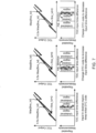
- the subranging measurement by TDC 110 solves the conflicting prior art problems of providing increased resolution over a wide input frequency range while maintaining a compact area and low circuit complexity. But the accuracy of its measurement depends upon the appropriate relationship between the periods of fast oscillator 210, the periods of the slow oscillator 205, and TDC input patterns. An ideal relationship results in a linear relationship between the input and output of TDC 110 as shown in Figure 5A for an implementation in which the fast oscillator output signal cycles five times faster than the slow oscillator signal.
- Coarse counter 220 ( Figure 2A ) will increment a single coarse quantizer integer step over which fine counter 225 ( Figure 2A ) will count five times. Since the slow and fast oscillator output signals are perfectly combined with knowledge of their accurate periods, the resulting output of TDC 110 (designated as the sum of the coarse and fine quantizer) is linear over an input range of 0 to 20.
- TDC 110 may be configured as shown in Figure 6 .
- Slow oscillator 205, fast oscillator 210, phase detector 215, coarse counter 220, and fine counter 220 function as discussed with regard to Figures 2A and 3 .
- the selected clock edge (designated as CK_in1) that triggers slow oscillator 205 is selectively delayed in a delay circuit that may also be designated as a digital-to-time converter (DTC) 610.
- DTC digital-to-time converter
- a histogram-based fine quantizer level detector and DTC tuning logic circuit 605 tunes DTC 610 using a first tuning code (Tune Coder) based upon the fine quantizer output from fine quantizer 225 and also the ratio (ratio_c2f) between the fine quantizer step size and the coarse quantizer step size. This ratio is known from the calibration of slow oscillator 205 and fast oscillator 210 discussed previously. The maximum fine quantizer value or output equals the ratio ratio_c2f. The desirable region for the TDC input is thus when fine quantizer 220 counts to approximately one-half of ratio_c2f. Referring again to Figure 5B , such a fine quantizer level results in an input-output relationship for TDC 110 that avoids the discontinuous regions.
- histogram-based fine quantizer level detector and DTC tuning logic circuit 605 observes the output of TDC 110 over a series of measurements such that the resulting histogram reveals whether the fine quantizer outputs for TDC 110 are occurring in the desired ratio_c2f/2 range for the corresponding coarse quantizer interval.
- the fine quantizer range over a coarse quantizer interval may be divided into 3 regions: a beginning interval ranging from 0 to .3*ratio_c2f, a central interval ranging from 0.3*ratio_c2f to 0.7*ratio_c2f, and a final interval ranging from 0.7*ratio_c2f to ratio_c2f.
- Some representative fine quantizer intervals for a coarse quantizer increment are shown in Figure 7 for three histograms of the fine quantizer count. In each histogram, the beginning and final intervals for a coarse quantizer increment are designated as undesired regions whereas the central interval for the same coarse quantizer increment is designated as the desired region. Each histogram is obtained from a series of repeated clock measurements. In a first histogram 700, the fine quantizer counts all occur in the desired region. There would be no reason to tune DTC 610 of Figure 6 given such a histogram result because the output of TDC 110 is avoiding the discontinuities in its input-output relationship as also illustrated in Figure 7 .
- a histogram 705 for the fine quantizer count results in all of the counts being in the initial undesired region.
- histogram-based fine quantizer level detector and DTC tuning logic circuit 605 may adjust the first tuning code so that DTC 610 adjusts delays of the first clock edge sufficiently so that a subsequent histogram measurement occurs with the fine quantizer counts landing in the desired region.
- Such an increase in time-difference at TDC input is appropriate to shift the fine quantizer counts from the initial undesirable range into the desirable range.
- histogram 710 results in the fine quantizer counts occurring in the final undesirable range such that histogram-based fine quantizer level detector and DTC tuning logic circuit 605 may adjust the first tuning code so that DTC 610 implements a reduced time-difference at TDC input. This reduction moves the resulting fine quantizer counts into the desired region.
- histogram-based fine quantizer level detector and DTC tuning logic circuit 605 may also tune a DTC 615 for adaptively delaying the second clock edge (designated as CK_in2) through a second tuning signal Tune codes. Such additional tuning is optional.
- a digital phase-locked loop 800 as shown in Figure 8 may include TDC 110 to compare an output clock signal CKV to a reference clock signal FREF to provide a variable phase output that is a digital word representing the phase difference between corresponding edges of the output clock signal CKV and the reference clock signal.
- An accumulator 805 produces a reference phase responsive to a frequency control word (FCW) and the reference clock signal.
- FCW frequency control word
- a loop filter 810 filters a phase error that equals the difference between the reference phase and the variable phase to produce a digital control word that controls the oscillation frequency of a digitally-controlled oscillator (DCO) 815 so as to control the frequency for output clock signal CKV.
- DCO digitally-controlled oscillator
- the DTC adjustment for TDC 110 in digital PLL 800 works well since typical jitter is much less that the coarse quantizer increment. Occasional outputs of TDC 110 that are affected by systematic error are filtered out by loop filter 800.
- the phase detection offset due to the DTC adjustment discussed with regard to Figures 6 and 7 is compensated by the loop feedback in digital PLL 800 once lock is obtained due to the resulting adjustment of the relative phase between the reference clock signal and a DCO clock signal (not illustrated). Since digital PLL 800 needs no reliance on oversampling and noise shaping its bandwidth for is advantageously high so as to help filter DCO noise and promotes fast settling and tracking.
Landscapes
- Physics & Mathematics (AREA)
- General Physics & Mathematics (AREA)
- Nonlinear Science (AREA)
- Engineering & Computer Science (AREA)
- Power Engineering (AREA)
- Stabilization Of Oscillater, Synchronisation, Frequency Synthesizers (AREA)
- Analogue/Digital Conversion (AREA)
- Manipulation Of Pulses (AREA)
- Measurement Of Unknown Time Intervals (AREA)
- Measuring Frequencies, Analyzing Spectra (AREA)
Applications Claiming Priority (3)
| Application Number | Priority Date | Filing Date | Title |
|---|---|---|---|
| US15/904,124 US10520901B2 (en) | 2018-02-23 | 2018-02-23 | Clock screening with programmable counter-based clock interface and time-to-digital converter with high resolution and wide range operation |
| PCT/US2019/014856 WO2019164626A2 (en) | 2018-02-23 | 2019-01-24 | Clock screening with programmable counter-based clock interface and time-to-digital converter with high resolution and wide range operation |
| EP19720210.4A EP3756276B1 (de) | 2018-02-23 | 2019-01-24 | Zeit-digital-wandler und verfahren zum messen der zeit zwischen taktflanken |
Related Parent Applications (1)
| Application Number | Title | Priority Date | Filing Date |
|---|---|---|---|
| EP19720210.4A Division EP3756276B1 (de) | 2018-02-23 | 2019-01-24 | Zeit-digital-wandler und verfahren zum messen der zeit zwischen taktflanken |
Publications (2)
| Publication Number | Publication Date |
|---|---|
| EP4472077A2 true EP4472077A2 (de) | 2024-12-04 |
| EP4472077A3 EP4472077A3 (de) | 2025-03-05 |
Family
ID=66323892
Family Applications (2)
| Application Number | Title | Priority Date | Filing Date |
|---|---|---|---|
| EP24188710.8A Pending EP4472077A3 (de) | 2018-02-23 | 2019-01-24 | Zeit-digital-wandler und verfahren zum messen der zeit zwischen taktflanken |
| EP19720210.4A Active EP3756276B1 (de) | 2018-02-23 | 2019-01-24 | Zeit-digital-wandler und verfahren zum messen der zeit zwischen taktflanken |
Family Applications After (1)
| Application Number | Title | Priority Date | Filing Date |
|---|---|---|---|
| EP19720210.4A Active EP3756276B1 (de) | 2018-02-23 | 2019-01-24 | Zeit-digital-wandler und verfahren zum messen der zeit zwischen taktflanken |
Country Status (4)
| Country | Link |
|---|---|
| US (2) | US10520901B2 (de) |
| EP (2) | EP4472077A3 (de) |
| CN (2) | CN111869106B (de) |
| WO (1) | WO2019164626A2 (de) |
Families Citing this family (22)
| Publication number | Priority date | Publication date | Assignee | Title |
|---|---|---|---|---|
| WO2019125300A1 (en) * | 2017-12-19 | 2019-06-27 | Huawei International Pte. Ltd. | Digital-to-time converter (dtc) assisted all digital phase locked loop (adpll) circuit |
| US10520901B2 (en) | 2018-02-23 | 2019-12-31 | Qualcomm Incorporated | Clock screening with programmable counter-based clock interface and time-to-digital converter with high resolution and wide range operation |
| US10886930B1 (en) * | 2019-07-30 | 2021-01-05 | Infineon Technologies Ag | Voltage controlled oscillator based analog-to-digital converter including a maximum length sequence generator |
| TWI733415B (zh) * | 2020-04-16 | 2021-07-11 | 瑞昱半導體股份有限公司 | 鎖相迴路裝置與時脈產生方法 |
| US10958257B1 (en) * | 2020-04-28 | 2021-03-23 | Taiwan Semiconductor Manufacturing Company Limited | System and method for adjusting duty cycle of a signal |
| JP7527946B2 (ja) * | 2020-12-11 | 2024-08-05 | 株式会社東芝 | 発振回路、時間デジタル変換器、及び電子装置 |
| US11356112B1 (en) * | 2021-01-27 | 2022-06-07 | Infineon Technologies Ag | Coarse-fine counting architecture for a VCO-ADC based on interlocked binary asynchronous counters |
| CN113219816B (zh) * | 2021-05-07 | 2022-05-17 | 中国科学技术大学 | 一种定时测量方法及时间数字变换器 |
| CN114675525B (zh) * | 2021-09-30 | 2022-09-02 | 绍兴圆方半导体有限公司 | 一种时间数字转换器和时钟同步系统 |
| CN114995093B (zh) * | 2021-09-30 | 2022-10-21 | 绍兴圆方半导体有限公司 | 时间数字转换器、处理周期信号的方法和信号处理系统 |
| CN114047682B (zh) * | 2021-11-16 | 2022-08-12 | 华南理工大学 | 一种有pvt鲁棒性基于全差分环形振荡器的时间数字转换器 |
| US12389356B2 (en) * | 2021-12-13 | 2025-08-12 | Intel Corporation | Opportunistic calibration of a clock |
| CN114967409B (zh) * | 2022-03-28 | 2023-06-20 | 中山大学 | 一种抗pvt变化的高精度时间数字转换器及其实现方法 |
| CN115118256B (zh) * | 2022-07-22 | 2025-11-14 | 东芯半导体股份有限公司 | 振荡周期匹配装置、方法、存储器及计算机可读取介质 |
| JP2024039785A (ja) * | 2022-09-12 | 2024-03-25 | 旭化成エレクトロニクス株式会社 | Td変換器およびpll回路 |
| CN116015286B (zh) * | 2022-12-31 | 2024-06-07 | 成都电科星拓科技有限公司 | 一种基于参考时钟周期获得dtc延迟步进的方法及装置 |
| CN116015284B (zh) * | 2022-12-31 | 2024-01-30 | 成都电科星拓科技有限公司 | 一种基于参考时钟周期获得tdc延迟步进的方法及装置 |
| CN116318128A (zh) * | 2023-03-30 | 2023-06-23 | 浙江地芯引力科技有限公司 | 数控振荡电路及振荡装置 |
| CN116614114B (zh) * | 2023-04-13 | 2023-12-19 | 浙江力积存储科技有限公司 | 延迟锁相环路时钟信号占空比检测方法、占空比检测器 |
| US12388430B1 (en) | 2024-02-13 | 2025-08-12 | Qualcomm Incorporated | Programmable delay-line circuit with single delay array and real-time calibration |
| CN118759498B (zh) * | 2024-06-20 | 2025-07-08 | 努美(天津)科技有限公司 | 一种基于差分进位链的快速tdc测量系统与方法 |
| CN120722173B (zh) * | 2025-08-27 | 2025-11-07 | 瀚博半导体(上海)股份有限公司 | 数字时钟抖动测量电路及测量方法 |
Family Cites Families (22)
| Publication number | Priority date | Publication date | Assignee | Title |
|---|---|---|---|---|
| US4072910A (en) * | 1976-04-09 | 1978-02-07 | Rca Corporation | Voltage controlled oscillator having equally controlled current source and current sink |
| US4164648A (en) * | 1978-06-23 | 1979-08-14 | Hewlett-Packard Company | Double vernier time interval measurement using triggered phase-locked oscillators |
| JP2868266B2 (ja) * | 1990-01-25 | 1999-03-10 | 株式会社日本自動車部品総合研究所 | 信号位相差検出回路及び信号位相差検出方法 |
| US5945883A (en) * | 1996-07-15 | 1999-08-31 | Mitsubishi Denki Kabushiki Kaisha | Voltage controlled ring oscillator stabilized against supply voltage fluctuations |
| US6295315B1 (en) | 1999-04-20 | 2001-09-25 | Arnold M. Frisch | Jitter measurement system and method |
| US6754613B2 (en) * | 2000-03-17 | 2004-06-22 | Vector 12 Corporation | High resolution time-to-digital converter |
| US7804925B2 (en) * | 2007-02-14 | 2010-09-28 | Infineon Technologies Ag | Detection arrangement, counter unit, phase locked loop, detection method and method for generating an oscillator signal |
| JP5590867B2 (ja) * | 2008-12-01 | 2014-09-17 | 三星電子株式会社 | タイム/デジタルコンバーター及びデジタル位相ロックループ |
| KR101632657B1 (ko) * | 2008-12-01 | 2016-06-23 | 삼성전자주식회사 | 타임투디지털 컨버터 및 디지털 위상 고정 루프 |
| WO2010150311A1 (ja) * | 2009-06-24 | 2010-12-29 | 富士通株式会社 | Tdc回路及びadpll回路 |
| CN103516367B (zh) * | 2012-06-20 | 2016-09-28 | 中国科学院电子学研究所 | 一种时间数字转换器 |
| JP6351058B2 (ja) * | 2013-11-28 | 2018-07-04 | 株式会社メガチップス | タイムデジタルコンバータ及びこれを用いたpll回路 |
| US9685940B2 (en) * | 2015-02-25 | 2017-06-20 | Qualcomm Incorporated | Voltage comparator |
| US9379714B1 (en) * | 2015-06-01 | 2016-06-28 | Liming Xiu | Circuits and methods of TAF-DPS vernier caliper for time-of-flight measurement |
| US9479150B1 (en) * | 2015-07-21 | 2016-10-25 | Realtek Semiconductor Corporation | Self-calibrating multi-phase clock circuit and method thereof |
| JP6859695B2 (ja) * | 2016-12-19 | 2021-04-14 | 富士通株式会社 | 情報処理装置、情報処理方法及び情報処理プログラム |
| US10175655B2 (en) * | 2017-03-17 | 2019-01-08 | Intel Corporation | Time-to-digital converter |
| US10473530B2 (en) * | 2017-08-18 | 2019-11-12 | Qualcomm Incorporated | Apparatus and method for generating temperature-indicating signal using correlated-oscillators |
| JP2019039673A (ja) * | 2017-08-22 | 2019-03-14 | セイコーエプソン株式会社 | 時間デジタル変換回路、回路装置、物理量測定装置、電子機器及び移動体 |
| JP2019039799A (ja) * | 2017-08-25 | 2019-03-14 | セイコーエプソン株式会社 | 時間デジタル変換回路、回路装置、物理量測定装置、電子機器及び移動体 |
| JP6939261B2 (ja) * | 2017-08-29 | 2021-09-22 | セイコーエプソン株式会社 | 時間デジタル変換回路、回路装置、物理量測定装置、電子機器及び移動体 |
| US10520901B2 (en) | 2018-02-23 | 2019-12-31 | Qualcomm Incorporated | Clock screening with programmable counter-based clock interface and time-to-digital converter with high resolution and wide range operation |
-
2018
- 2018-02-23 US US15/904,124 patent/US10520901B2/en active Active
-
2019
- 2019-01-24 CN CN201980014849.5A patent/CN111869106B/zh active Active
- 2019-01-24 EP EP24188710.8A patent/EP4472077A3/de active Pending
- 2019-01-24 EP EP19720210.4A patent/EP3756276B1/de active Active
- 2019-01-24 CN CN202411316223.9A patent/CN119148493A/zh active Pending
- 2019-01-24 WO PCT/US2019/014856 patent/WO2019164626A2/en not_active Ceased
- 2019-11-14 US US16/684,421 patent/US10707854B2/en active Active
Also Published As
| Publication number | Publication date |
|---|---|
| WO2019164626A2 (en) | 2019-08-29 |
| CN119148493A (zh) | 2024-12-17 |
| CN111869106A (zh) | 2020-10-30 |
| EP4472077A3 (de) | 2025-03-05 |
| EP3756276C0 (de) | 2024-07-17 |
| US10707854B2 (en) | 2020-07-07 |
| WO2019164626A3 (en) | 2019-11-14 |
| CN111869106B (zh) | 2024-10-11 |
| EP3756276A2 (de) | 2020-12-30 |
| EP3756276B1 (de) | 2024-07-17 |
| US20190268010A1 (en) | 2019-08-29 |
| US20200083873A1 (en) | 2020-03-12 |
| US10520901B2 (en) | 2019-12-31 |
Similar Documents
| Publication | Publication Date | Title |
|---|---|---|
| US10707854B2 (en) | Clock screening with programmable counter-based clock interface and time-to-digital converter with high resolution and wide range operation | |
| JP5590867B2 (ja) | タイム/デジタルコンバーター及びデジタル位相ロックループ | |
| US8797203B2 (en) | Low-power high-resolution time-to-digital converter | |
| US9543970B2 (en) | Circuit for digitizing phase differences, PLL circuit and method for the same | |
| KR101632657B1 (ko) | 타임투디지털 컨버터 및 디지털 위상 고정 루프 | |
| US10171089B2 (en) | PVT-free calibration function using a doubler circuit for TDC resolution in ADPLL applications | |
| JP5347534B2 (ja) | 位相比較器、pll回路、及び位相比較器の制御方法 | |
| US12149264B2 (en) | Loop gain auto calibration using loop gain detector | |
| CN118801875A (zh) | 双模锁相环电路、振荡电路及振荡电路的控制方法 | |
| US11533058B2 (en) | Digital phase-frequency detector with split control loops for low jitter and fast locking | |
| CN110518906B (zh) | 信号生成电路及其方法、数字时间转换电路及其方法 | |
| US9698807B1 (en) | Time signal conversion using dual time-based digital-to-analog converters | |
| US6897691B2 (en) | Phase locked loop with low steady state phase errors and calibration circuit for the same | |
| CN107026647B (zh) | 时间数字系统以及频率合成器 | |
| JP5333439B2 (ja) | 周波数シンセサイザおよび発振器の発振周波数制御方法 | |
| CN110518907A (zh) | 信号生成电路及其方法、数字时间转换电路及其方法 | |
| Nisa'Minhad et al. | Investigating phase detectors: Advances in mature and emerging phase-frequency and time-to-digital detectors in phase-locked looped systems | |
| CN117097338A (zh) | 一种基于可调延时精度tdc的电压数字转换电路 | |
| Huang et al. | A time-to-digital converter based AFC for wideband frequency synthesizer | |
| CN113193868A (zh) | 锁相检测装置和锁相检测方法、锁相环 | |
| CN104539288A (zh) | 可调节分辨率的tdc及基于该tdc的adpll | |
| CN215186702U (zh) | 锁相检测装置、锁相环 | |
| CN119543932A (zh) | 一种锁相环电路、锁定检测电路和方法 |
Legal Events
| Date | Code | Title | Description |
|---|---|---|---|
| PUAI | Public reference made under article 153(3) epc to a published international application that has entered the european phase |
Free format text: ORIGINAL CODE: 0009012 |
|
| STAA | Information on the status of an ep patent application or granted ep patent |
Free format text: STATUS: REQUEST FOR EXAMINATION WAS MADE |
|
| 17P | Request for examination filed |
Effective date: 20240815 |
|
| AC | Divisional application: reference to earlier application |
Ref document number: 3756276 Country of ref document: EP Kind code of ref document: P |
|
| AK | Designated contracting states |
Kind code of ref document: A2 Designated state(s): AL AT BE BG CH CY CZ DE DK EE ES FI FR GB GR HR HU IE IS IT LI LT LU LV MC MK MT NL NO PL PT RO RS SE SI SK SM TR |
|
| REG | Reference to a national code |
Ref country code: DE Ref legal event code: R079 Free format text: PREVIOUS MAIN CLASS: H03K0003030000 Ipc: G04F0010000000 |
|
| PUAL | Search report despatched |
Free format text: ORIGINAL CODE: 0009013 |
|
| AK | Designated contracting states |
Kind code of ref document: A3 Designated state(s): AL AT BE BG CH CY CZ DE DK EE ES FI FR GB GR HR HU IE IS IT LI LT LU LV MC MK MT NL NO PL PT RO RS SE SI SK SM TR |
|
| RIC1 | Information provided on ipc code assigned before grant |
Ipc: H03K 3/03 20060101ALI20250128BHEP Ipc: H03K 3/011 20060101ALI20250128BHEP Ipc: H03K 5/26 20060101ALI20250128BHEP Ipc: G04F 10/00 20060101AFI20250128BHEP |