EP4465439A1 - Waveguide with a curved-wall low-pass filter - Google Patents
Waveguide with a curved-wall low-pass filter Download PDFInfo
- Publication number
- EP4465439A1 EP4465439A1 EP23182496.2A EP23182496A EP4465439A1 EP 4465439 A1 EP4465439 A1 EP 4465439A1 EP 23182496 A EP23182496 A EP 23182496A EP 4465439 A1 EP4465439 A1 EP 4465439A1
- Authority
- EP
- European Patent Office
- Prior art keywords
- waveguide
- output port
- input port
- low
- bottom wall
- Prior art date
- Legal status (The legal status is an assumption and is not a legal conclusion. Google has not performed a legal analysis and makes no representation as to the accuracy of the status listed.)
- Pending
Links
Images




Classifications
-
- H—ELECTRICITY
- H01—ELECTRIC ELEMENTS
- H01P—WAVEGUIDES; RESONATORS, LINES, OR OTHER DEVICES OF THE WAVEGUIDE TYPE
- H01P1/00—Auxiliary devices
- H01P1/20—Frequency-selective devices, e.g. filters
- H01P1/207—Hollow waveguide filters
- H01P1/208—Cascaded cavities; Cascaded resonators inside a hollow waveguide structure
- H01P1/2088—Integrated in a substrate
-
- H—ELECTRICITY
- H01—ELECTRIC ELEMENTS
- H01P—WAVEGUIDES; RESONATORS, LINES, OR OTHER DEVICES OF THE WAVEGUIDE TYPE
- H01P3/00—Waveguides; Transmission lines of the waveguide type
-
- H—ELECTRICITY
- H01—ELECTRIC ELEMENTS
- H01P—WAVEGUIDES; RESONATORS, LINES, OR OTHER DEVICES OF THE WAVEGUIDE TYPE
- H01P1/00—Auxiliary devices
- H01P1/02—Bends; Corners; Twists
- H01P1/022—Bends; Corners; Twists in waveguides of polygonal cross-section
-
- H—ELECTRICITY
- H01—ELECTRIC ELEMENTS
- H01P—WAVEGUIDES; RESONATORS, LINES, OR OTHER DEVICES OF THE WAVEGUIDE TYPE
- H01P1/00—Auxiliary devices
- H01P1/20—Frequency-selective devices, e.g. filters
- H01P1/207—Hollow waveguide filters
-
- H—ELECTRICITY
- H01—ELECTRIC ELEMENTS
- H01P—WAVEGUIDES; RESONATORS, LINES, OR OTHER DEVICES OF THE WAVEGUIDE TYPE
- H01P1/00—Auxiliary devices
- H01P1/20—Frequency-selective devices, e.g. filters
- H01P1/207—Hollow waveguide filters
- H01P1/209—Hollow waveguide filters comprising one or more branching arms or cavities wholly outside the main waveguide
Definitions
- Some devices use electromagnetic (EM) signals to detect and track objects.
- EM signals are transmitted and received using antennas which may be characterized in terms of gains, beam widths, or, more specifically, in terms of antenna patterns, which are measures of the antenna gains as functions of directions.
- Waveguides are often used to change or improve the antenna patterns.
- Waveguides often have various structures designed to guide, balance, or filter the EM signals.
- a filter may be used to keep undesired signals from entering a portion of a waveguide.
- These filters are often hard to manufacture and/or are long structures in order to achieve good rejection properties, which makes them potentially expensive options in both cost and/or space.
- a waveguide comprising a low-pass filter portion configured to allow low-frequency electromagnetic energy therethrough and reject high-frequency electromagnetic energy.
- the low-pass filter portion comprises: an input port; an output port; and a cavity feature formed between the input port and the output port.
- the cavity feature has a greater depth than respective depths of the input port and the output port.
- the cavity feature comprises a top wall and a bottom wall that is disposed opposite the top wall, that achieves the greater depth for the cavity feature.
- the bottom wall comprises at least one curved portion configured to allow the cavity feature to achieve the allowance of the low-frequency electromagnetic energy and the rejection of the high-frequency electromagnetic energy.
- a length of the cavity feature between the input port and the output port may be less than two times an operating wavelength.
- the greater depth of the cavity feature may be approximately an operating wavelength.
- the greater depth of the cavity feature may be approximately half a length of the cavity feature.
- the input port and the output port may have different depths.
- the top wall may comprise a jog portion between two parallel portions to achieve the different depths.
- the jog portion may be halfway between the input port and the output port or offset from a halfway point between the input port and the output port.
- the bottom wall may further comprise a flat portion that is parallel to at least a portion of the top wall, the flat portion providing the greater depth.
- the bottom wall may further comprise a first curved portion that connects the input port to the flat portion and a second curved portion that connects the output port to the flat portion.
- the first curved portion and the second curved portion may be cylindrical.
- a first end of the first curved portion may be tangent with the input port, and a first end of the second curved portion may be tangent with the output port.
- a second end of the first curved portion may be substantially normal with the flat portion, and a second end of the second curved portion may be substantially normal with the flat portion.
- the bottom wall may be elliptical to form the greater depth.
- a first end of the bottom wall may be substantially normal with the input port, and a second end of the bottom wall may be substantially normal with the output port.
- the bottom wall may comprise a first elliptical portion and a second elliptical portion, where the first and second elliptical portions form the greater depth.
- a first end of the first elliptical portion may be substantially normal with the input port, and a second the second elliptical portion may be substantially normal with the output port.
- the first elliptical portion and the second elliptical portion may meet forming an extension portion that extends towards the top wall away from the greater depth.
- the extension portion may extend less than half a distance from a bottom extent of the bottom wall to the input port or output port.
- a system comprising a processor configured to generate low-frequency electromagnetic energy and a waveguide as described above that is configured to guide the low-frequency electromagnetic energy and reject high-frequency electromagnetic energy.
- a waveguide with a curved-wall low-pass filter is described with reference to the following drawings that use some of the same numbers throughout to reference like or examples of like features and components.
- Waveguides often have various structures designed to guide, balance, or filter EM signals.
- a filter may be used to keep undesired signals (e.g., higher frequency signals) from entering a portion of a waveguide (e.g., one configured for lower-frequency signals).
- Such filters are often hard to manufacture and/or are long structures in order to achieve good rejection properties, which makes them potentially expensive options in both cost and/or space.
- thin iris filters are often implemented in waveguides; however, they require fine machining, which may be expensive.
- Stepped impedance filters do not require irises; however, they are very long structures, which means that they are often space prohibitive.
- notch filters have been developed; however, they often have very narrow rejection bands.
- a waveguide with a curved-wall low-pass filter is described herein.
- the waveguide comprises a low-pass filter portion configured to allow low-frequency electromagnetic energy therethrough and reject high-frequency electromagnetic energy.
- the low-pass filter portion comprises an input port, an output port, and a cavity feature that is formed between the input port and the output port.
- the cavity feature has a greater depth than respective depths of the input port and the output port.
- the cavity feature comprises a bottom wall that achieves the greater depth for the cavity feature.
- the bottom wall comprises at least one curved portion configured to allow the cavity feature to achieve the allowance of the low-frequency electromagnetic energy and the rejection of the high-frequency electromagnetic energy.
- the cavity feature may allow the waveguide to have as good or better performance than conventional means (e.g., at least 10 dB rejection within 2 gigahertz (GHz) and for a bandwidth of at least 5 GHz) while being easier to manufacture and/or taking up less space. Doing so may save costs while also allowing for a smaller footprint on the vehicles in which the waveguide is deployed.
- conventional means e.g., at least 10 dB rejection within 2 gigahertz (GHz) and for a bandwidth of at least 5 GHz
- Fig. 1 illustrates an example environment 100 where a waveguide with a curved-wall low-pass filter may be used.
- Example environment 100 contains a radar system 102 that is disposed within, disposed on, or dispersed throughout a vehicle 104.
- the radar system 102 contains a waveguide 106 (e.g., a waveguide with a curved-wall low-pass filter) that may be used by the radar system 102 to perform various sensing tasks related to object(s) 108 that are within a fields-of-view 110 of the radar system 102.
- a waveguide 106 e.g., a waveguide with a curved-wall low-pass filter
- the vehicle 104 may represent other types of motorized vehicles (e.g., a motorcycle, a bus, a tractor, a semi-trailer truck, construction equipment), non-motorized vehicles (e.g., a bicycle), railed vehicles (e.g., a train or a trolley car), watercraft (e.g., a boat or a ship), aircraft (e.g., an airplane or a helicopter), or spacecraft (e.g., satellite).
- manufacturers may mount the radar system 102 to any moving platform, including moving machinery or robotic equipment.
- other devices e.g., desktop computers, tablets, laptops, televisions, computing watches, smartphones, gaming systems
- the radar system 102 may incorporate the radar system 102 with the waveguide 106 and support techniques described herein.
- the radar system 102 also includes one or more processors (not illustrated) and computer-readable storage media (CRM) (not illustrated).
- the processor may be a microprocessor or a system-on-chip.
- the processor executes instructions stored within the CRM.
- the processor controls the operation of a transmitter (not illustrated) that is connected to waveguide 106.
- the processor may also process signals (EM signals/energy) received via the waveguide 106 and determine information about the objects 108.
- the processor may also generate radar data for the automotive systems.
- the processor controls or directs operations of an autonomous or semi-autonomous driving system of vehicle 104.
- the radar system 102 may include a monolithic microwave integrated circuit (MMIC) that interfaces with the waveguide 106.
- MMIC monolithic microwave integrated circuit
- the radar system 102 may detect and track the objects 108 by operating in different frequency modes and/or polarizations.
- a low-frequency mode may use low-frequency radar signals (e.g., 76.5 GHz) and a horizontally polarized antenna array to create the field-of-view 110 with a wide azimuth and a long range (e.g., configured for medium and long-range detections).
- the low-frequency mode may be used, for example, as an imaging radar. It should be noted that the low-frequency mode could use a single and/or vertically polarized antenna(s).
- the operating frequencies may vary without departing from the scope of this disclosure.
- the waveguide 106 provides electromagnetic energy paths through the waveguide 106.
- the energy paths are formed by a feed portion 112 and a low-frequency portion 114.
- the waveguide 106 has a low-frequency energy path.
- Feed portion 112 contains a feed port 120 that is configured to interface with a transmitter/receiver (e.g., MMIC).
- the low-frequency portion 114 contains a low-pass filter 122 and low-frequency antenna(s) 124.
- the low-pass filter 122 is configured to block high-frequency radar signals (or other signals) from entering the low-frequency portion 114 and ultimately from reaching the low-frequency antenna(s) 124.
- Figs. 2 and 3 illustrate a first example of the low-pass filter 122.
- the low-pass filter 122 has a filter input port 200 and a filter output port 202. Between the filter input port 200 and the filter output port 202 are a top wall 204 and a bottom wall 206.
- the bottom wall 206 is opposite the top wall 204 and forms a greater depth 208 (e.g., in the z direction) than either of the filter input port 200 or the filter output port 202.
- An area between the filter input port 200 the filter output port 202 forms a cavity 210.
- the waveguide 106 may be easily manufacturable (e.g., in two pieces) with minimal signal loss through the separation plane 212.
- edges are filleted for ease of manufacturing.
- the edges may also be squared (or chamfered) without departing from the scope of this disclosure.
- bottom wall 206 comprises a flat portion 214 and curved portions 216.
- the flat portion 214 may be parallel to the top wall 204 and be between the curved portions 216.
- the curved portions 216 may be cylindrical in shape (e.g., having a constant radius) or non-cylindrical in shape (e.g., having a varying radius).
- the curved portions 216 may be convex from the perspective of cavity 210. In other words, cavity 210 may have a wider profile (e.g., in the x direction) near the filter input port 200 and the filter output port 202 than toward the flat portion 214.
- the curved portions 216 may meet the filter input port 200 and the filter output port 202 at tangent angles (e.g., be parallel) and the flat portion 214 at or near perpendicular angles. Depending on the radius(es) used and the dimensions of the low-pass filter 122, the curved portions 216 may meet the flat portion 214 at non-perpendicular angles.
- the transition from the curved portions 216 to the flat portion 214 may be filleted (as shown), chamfered with smaller radius fillets, chamfered with edges, or along an edge (e.g., not filleted or chamfered).
- the greater depth 208 may be less than half a length 220 (e.g., in the x direction) of the cavity 210 between the filter input port 200 and the filter output port 202.
- the length 220 may be less than two times an operating wavelength (e.g., of the low-frequency portion 114).
- the filter input port 200 and the filter output port 202 may have similar or different dimensions.
- the top wall 204 may have a jog that causes the filter output port 202 to have a lesser depth than the filter input port 200.
- the jog may have a flat portion that is angled relative to other portions of the top wall 204 or be a smooth curve.
- the jog may be centered between the filter input port 200 and the filter output port 202 or be offset.
- the jog may be offset towards the filter input port 200 or the filter output port 202.
- the jog may be configured to widen the rejection band of the low-pass filter 122.
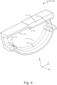
- Figs. 4 and 5 illustrate a second example of the low-pass filter 122.
- the low-pass filter 122 has the filter input port 200 and the filter output port 202. Between the filter input port 200 and the filter output port 202 are the top wall 204 and the bottom wall 206. The bottom wall 206 is opposite the top wall 204 and forms the greater depth 208 (e.g., in the z direction) than either of the filter input port 200 or the filter output port 202. An area between the filter input port 200 the filter output port 202 forms the cavity 210.
- the waveguide 106 may be easily manufacturable (e.g., in two pieces) with minimal signal loss through the separation plane 212.
- edges are filleted for ease of manufacturing.
- the edges may also be squared (or chamfered) without departing from the scope of this disclosure.
- bottom wall 206 comprises a single curved surface (minus transitions to the filter input port 200 and the filter output port 202.
- the bottom wall 206 may be elliptical in shape (as shown).
- the bottom wall 206 may meet the filter input port 200 and the filter output port 202 at or near right angles. Depending on the elliptical dimensions used and the dimensions of the low-pass filter 122, the bottom wall 206 may meet the filter input port 200 and the filter output port 202 at non-right angles.
- the transition from the bottom wall 206 to the filter input port 200 and the filter output port 202 may be filleted, chamfered with smaller radius fillets (as shown), chamfered with edges, or along an edge (e.g., not filleted or chamfered).
- the greater depth 208 may be less than half a length 220 (e.g., in the x direction) of the cavity 210 between the filter input port 200 and the filter output port 202.
- the length 220 may be less than two times an operating wavelength (e.g., of the low-frequency portion 114).
- the filter input port 200 and the filter output port 202 may have similar or different dimensions.
- the top wall 204 may have the jog 400 (as illustrated) that causes the filter output port 202 to have a lesser depth than the filter input port 200.
- the jog 400 may have a flat portion (as shown) that is at an angle relative to the rest of the top wall 204 or be a smooth curve.
- the jog 400 may be centered between the filter input port 200 and the filter output port 202 or be offset (as shown). For example, the jog may be offset towards the filter input port 200 (as shown) or towards the filter output port 202.
- the jog 400 may be configured to widen the rejection band of the low-pass filter 122.
- Figs. 6 and 7 illustrate a third example of the low-pass filter 122.
- the low-pass filter 122 has the filter input port 200 and the filter output port 202. Between the filter input port 200 and the filter output port 202 are the top wall 204 and the bottom wall 206. The bottom wall 206 is opposite the top wall 204 and forms a greater depth 208 (e.g., in the z direction) than either of the filter input port 200 or the filter output port 202. An area between the filter input port 200 the filter output port 202 forms the cavity 210.
- the waveguide 106 may be easily manufacturable (e.g., in two pieces) with minimal signal loss through the separation plane 212.
- edges are filleted for ease of manufacturing.
- the edges may also be squared (or chamfered) without departing from the scope of this disclosure.
- the bottom wall 206 comprises elliptical portions 600 that join in an extension portion 602.
- the extension portion 602 may extend toward the top wall 204.
- the height of the extension portion 602 (e.g., away from deepest extents of the elliptical portions 600) may vary without departing from the scope of this disclosure.
- the elliptical portions 600 may be convex from the perspective of cavity 210. In other words, cavity 210 may have a wider profile (e.g., in the x direction) near the filter input port 200 and the filter output port 202 than toward extents of the elliptical portions 600 away from the top wall 204.
- the bottom wall 206 may meet the filter input port 200 and the filter output port 202 at or near right angles. Depending on the elliptical dimensions used and the dimensions of the low-pass filter 122, the bottom wall 206 may meet the filter input port 200 and the filter output port 202 at non-right angles.
- the transition from the bottom wall 206 to the filter input port 200 and the filter output port 202 may be filleted (as shown), chamfered with smaller radius fillets, chamfered with edges, or along an edge (e.g., not filleted or chamfered).
- the greater depth 208 (e.g., from the top wall 204 to deepest extents of the elliptical portions 600) may be less than half a length 220 (e.g., in the x direction) of the cavity 210 between the filter input port 200 and the filter output port 202.
- the length 220 may be less than two times an operating wavelength (e.g., of the low-frequency portion 114).
- the filter input port 200 and the filter output port 202 may have similar or different dimensions.
- the top wall 204 may have the jog 400 (as illustrated) that causes the filter output port 202 to have a lesser depth than the filter input port 200.
- the jog 400 may have a flat portion that is at an angle relative to the rest of the top wall 204 or be a smooth curve (as shown).
- the jog 400 may be centered between the filter input port 200 and the filter output port 202 or be offset (as shown).
- the jog may be offset towards the filter input port 200 or towards the filter output port 202 (as shown).
- the jog 400 may be configured to widen the rejection band of the low-pass filter 122.
- Fig. 8 illustrates an example method 800 of forming and implementing a waveguide with a curved-wall low-pass filter.
- the order in which the operations are shown and/or described is not intended to be construed as a limitation, and the order may be rearranged without departing from the scope of this disclosure. Furthermore, any number of the operations can be combined with any other number of the operations to implement the example process flow or an alternate process flow
- a waveguide comprising a curved-wall low-pass filter is formed.
- waveguide 106 may be formed such that it contains low-pass filter with the cavity.
- the waveguide 106 may be formed of one or more pieces.
- the waveguide 106 may be formed of multiple pieces that are adhered or bonded together (e.g., along a center plane). To do so, one or more pieces of the waveguide 106 may be formed using computer numeric control (CNC), injection molding, casting, machining, or any other manufacturing process and may be formed of metal or plastic.
- CNC computer numeric control
- surfaces of the waveguide 106 may be metallicized (e.g., if the waveguide 106 is formed of a non-conductive material).
- the pieces When formed of multiple pieces, the pieces may be glued/bonded (using a non-conductive adhesive), bolted, screwed (e.g., using one or more screws), snapped (e.g., using one or more snaps), welded, clamped using one or more clamps, press-fit, or any other assembly process known by those of ordinary skill in the art to form the waveguide 106.
- waveguide 106 is integrated into a radar system of a vehicle.
- the waveguide 106 may be integrated within the radar system 102 of the vehicle 104.
- the waveguide is utilized to detect objects in an environment of the vehicle.
- the low-pass filter 122 may be utilized as part of the low-frequency portion 114 to detect objects at far ranges and wide azimuth angles (e.g., field-of-view 110A).
- Example 1 A waveguide comprising: a low-pass filter portion configured to allow low-frequency electromagnetic energy therethrough and reject high-frequency electromagnetic energy, the low-pass filter portion comprising: an input port; an output port; and a cavity feature formed between the input port and the output port, the cavity feature having a greater depth than respective depths of the input port and the output port, the cavity feature comprising: a top wall; and a bottom wall, disposed opposite the top wall, that achieves the greater depth for the cavity feature, the bottom wall comprising at least one curved portion configured to allow the cavity feature to achieve the allowance of the low-frequency electromagnetic energy and the rejection of the high-frequency electromagnetic energy.
- Example 2 The waveguide of example 1, wherein a length of the cavity feature between the input port and the output port is less than two times an operating wavelength.
- Example 3 The waveguide of example 1 or 2, wherein the greater depth of the cavity feature is approximately an operating wavelength.
- Example 4 The waveguide of example 1, 2, or 3, wherein the greater depth of the cavity feature is approximately half a length of the cavity feature.
- Example 5 The waveguide of any preceding example, wherein the input port and the output port have different depths.
- Example 6 The waveguide of example 5, wherein the top wall comprises a jog feature between two parallel portions.
- Example 7 The waveguide of example 6, wherein the jog feature is halfway between the input port and the output port.
- Example 8 The waveguide of any preceding example, wherein the bottom wall further comprises: a flat portion that is parallel to at least a portion of the top wall, the flat portion providing the greater depth; a first curved portion that connects the input port to the flat portion; and a second curved portion that connects the output port to the flat portion.
- Example 9 The waveguide of example 8, wherein the first curved portion and the second curved portion are cylindrical.
- Example 10 The waveguide of example 9, wherein: a first end of the first curved portion is tangent with the input port; and a second end of the second curved portion is tangent with the output port.
- Example 11 The waveguide of example 9, wherein: a second end of the first curved portion is substantially normal with the flat portion; and a first end of the second curved portion is substantially normal with the flat portion.
- Example 12 The waveguide of any preceding example, wherein the bottom wall is elliptical to form the greater depth.
- Example 13 The waveguide of example 12, wherein: a first end of the bottom wall is substantially normal with the input port; and a second end of the bottom wall is substantially normal with the output port.
- Example 14 The waveguide of any preceding example, wherein the bottom wall comprises a first elliptical portion and a second elliptical portion, the first and second elliptical portions forming the greater depth.
- Example 15 The waveguide of example 14, wherein: a first end of the first elliptical portion is substantially normal with the input port; and a second end of the second elliptical portion is substantially normal with the output port.
- Example 16 The waveguide of example 14, wherein the first elliptical portion and the second elliptical portion meet forming an extension portion that extends towards the top wall away from the greater depth.
- Example 17 The waveguide of example 16, wherein the extension portion extends less than half a distance from a bottom extent of the bottom wall to the input port or output port.
- Example 18 A system comprising: a processor configured to generate low-frequency electromagnetic energy; and a waveguide configured to guide the low-frequency electromagnetic energy, the waveguide comprising: a low-pass filter portion configured to allow low-frequency electromagnetic energy therethrough and reject high-frequency electromagnetic energy, the low-pass filter portion comprising: an input port; an output port; and a cavity feature formed between the input port and the output port, the cavity feature having a greater depth than respective depths of the input port and the output port, the cavity feature comprising: a top wall; and a bottom wall, disposed opposite the top wall, that achieves the greater depth for the cavity feature, the bottom wall comprising at least one curved portion configured to allow the cavity feature to achieve the allowance of the low-frequency electromagnetic energy and the rejection of the high-frequency electromagnetic energy.
- Example 19 The system of example 18, wherein the bottom wall is elliptical to form the greater depth.
- Example 20 The system of example 18 or 19, wherein the bottom wall comprises a first elliptical portion and a second elliptical portion, the first and second elliptical portions forming the greater depth.
- "at least one of: a, b, or c” is intended to cover a, b, c, a-b, a-c, b-c, and a-b-c, as well as any combination with multiples of the same element (e.g., a-a, a-a-a, a-a-b, a-a-c, a-b-b, a-c-c, b-b, b-b-b, b-b-c, c-c, and c-c-c or any other ordering of a, b, and c).
Landscapes
- Control Of Motors That Do Not Use Commutators (AREA)
Abstract
A waveguide with a curved-wall low-pass filter is described herein. The waveguide comprises a low-pass filter portion configured to allow low-frequency electromagnetic energy therethrough and reject high-frequency electromagnetic energy. The low-pass filter portion comprises an input port, an output port, and a cavity feature that is formed between the input port and the output port. The cavity feature has a greater depth than respective depths of the input port and the output port. The cavity feature comprises a bottom wall that achieves the greater depth for the cavity feature. The bottom wall comprises at least one curved portion configured to allow the cavity feature to achieve the allowance of the low-frequency electromagnetic energy and the rejection of the high-frequency electromagnetic energy. The cavity feature may allow the waveguide to have as good or better performance than traditional means while being easier to manufacture and/or taking up less space.
Description
- Some devices (e.g., radar devices) use electromagnetic (EM) signals to detect and track objects. The EM signals are transmitted and received using antennas which may be characterized in terms of gains, beam widths, or, more specifically, in terms of antenna patterns, which are measures of the antenna gains as functions of directions. Waveguides are often used to change or improve the antenna patterns.
- Waveguides often have various structures designed to guide, balance, or filter the EM signals. For example, a filter may be used to keep undesired signals from entering a portion of a waveguide. These filters are often hard to manufacture and/or are long structures in order to achieve good rejection properties, which makes them potentially expensive options in both cost and/or space.
- This document is directed to a waveguide with a curved-wall low-pass filter. Some aspects described below include a waveguide comprising a low-pass filter portion configured to allow low-frequency electromagnetic energy therethrough and reject high-frequency electromagnetic energy. The low-pass filter portion comprises: an input port; an output port; and a cavity feature formed between the input port and the output port. The cavity feature has a greater depth than respective depths of the input port and the output port. The cavity feature comprises a top wall and a bottom wall that is disposed opposite the top wall, that achieves the greater depth for the cavity feature. The bottom wall comprises at least one curved portion configured to allow the cavity feature to achieve the allowance of the low-frequency electromagnetic energy and the rejection of the high-frequency electromagnetic energy.
- In some implementations, a length of the cavity feature between the input port and the output port may be less than two times an operating wavelength.
- In some implementations, the greater depth of the cavity feature may be approximately an operating wavelength.
- In some implementations, the greater depth of the cavity feature may be approximately half a length of the cavity feature.
- In some implementations, the input port and the output port may have different depths. The top wall may comprise a jog portion between two parallel portions to achieve the different depths. The jog portion may be halfway between the input port and the output port or offset from a halfway point between the input port and the output port.
- In some implementations, the bottom wall may further comprise a flat portion that is parallel to at least a portion of the top wall, the flat portion providing the greater depth. The bottom wall may further comprise a first curved portion that connects the input port to the flat portion and a second curved portion that connects the output port to the flat portion. The first curved portion and the second curved portion may be cylindrical. A first end of the first curved portion may be tangent with the input port, and a first end of the second curved portion may be tangent with the output port. A second end of the first curved portion may be substantially normal with the flat portion, and a second end of the second curved portion may be substantially normal with the flat portion.
- In some implementations, the bottom wall may be elliptical to form the greater depth. A first end of the bottom wall may be substantially normal with the input port, and a second end of the bottom wall may be substantially normal with the output port.
- In some implementations, the bottom wall may comprise a first elliptical portion and a second elliptical portion, where the first and second elliptical portions form the greater depth. A first end of the first elliptical portion may be substantially normal with the input port, and a second the second elliptical portion may be substantially normal with the output port. The first elliptical portion and the second elliptical portion may meet forming an extension portion that extends towards the top wall away from the greater depth. The extension portion may extend less than half a distance from a bottom extent of the bottom wall to the input port or output port.
- Other aspects described below include a system comprising a processor configured to generate low-frequency electromagnetic energy and a waveguide as described above that is configured to guide the low-frequency electromagnetic energy and reject high-frequency electromagnetic energy.
- This Summary introduces simplified concepts of a waveguide with a curved-wall low-pass filter that is further described in the Detailed Description and Drawings. This Summary is not intended to identify essential features of the claimed subject matter, nor is it intended for use in determining the scope of the claimed subject matter.
- A waveguide with a curved-wall low-pass filter is described with reference to the following drawings that use some of the same numbers throughout to reference like or examples of like features and components.
-
Fig. 1 illustrates, in accordance with this disclosure, an example environment where a waveguide with a curved-wall low-pass filter may be used. -
Fig. 2 illustrates, in accordance with this disclosure, a first example of a curved-wall low-pass filter. -
Fig. 3 illustrates, in accordance with this disclosure, another view of the first example of a curved-wall low-pass filter. -
Fig. 4 illustrates, in accordance with this disclosure, a second example of a curved-wall low-pass filter. -
Fig. 5 illustrates, in accordance with this disclosure, another view of the second example of a curved-wall low-pass filter. -
Fig. 6 illustrates, in accordance with this disclosure, a third example of a curved-wall low-pass filter. -
Fig. 7 illustrates, in accordance with this disclosure, another view of the third example of a curved-wall low-pass filter. -
Fig. 8 illustrates, in accordance with this disclosure, an example method of forming and implementing a waveguide with a curved-wall low-pass filter. - Waveguides often have various structures designed to guide, balance, or filter EM signals. For example, a filter may be used to keep undesired signals (e.g., higher frequency signals) from entering a portion of a waveguide (e.g., one configured for lower-frequency signals). Such filters are often hard to manufacture and/or are long structures in order to achieve good rejection properties, which makes them potentially expensive options in both cost and/or space.
- For example, thin iris filters are often implemented in waveguides; however, they require fine machining, which may be expensive. Stepped impedance filters do not require irises; however, they are very long structures, which means that they are often space prohibitive. Further, notch filters have been developed; however, they often have very narrow rejection bands.
- A waveguide with a curved-wall low-pass filter is described herein. The waveguide comprises a low-pass filter portion configured to allow low-frequency electromagnetic energy therethrough and reject high-frequency electromagnetic energy. The low-pass filter portion comprises an input port, an output port, and a cavity feature that is formed between the input port and the output port. The cavity feature has a greater depth than respective depths of the input port and the output port. The cavity feature comprises a bottom wall that achieves the greater depth for the cavity feature. The bottom wall comprises at least one curved portion configured to allow the cavity feature to achieve the allowance of the low-frequency electromagnetic energy and the rejection of the high-frequency electromagnetic energy.
- The cavity feature may allow the waveguide to have as good or better performance than conventional means (e.g., at least 10 dB rejection within 2 gigahertz (GHz) and for a bandwidth of at least 5 GHz) while being easier to manufacture and/or taking up less space. Doing so may save costs while also allowing for a smaller footprint on the vehicles in which the waveguide is deployed.
-
Fig. 1 illustrates anexample environment 100 where a waveguide with a curved-wall low-pass filter may be used.Example environment 100 contains aradar system 102 that is disposed within, disposed on, or dispersed throughout avehicle 104. Theradar system 102 contains a waveguide 106 (e.g., a waveguide with a curved-wall low-pass filter) that may be used by theradar system 102 to perform various sensing tasks related to object(s) 108 that are within a fields-of-view 110 of theradar system 102. - Although illustrated as a car, the
vehicle 104 may represent other types of motorized vehicles (e.g., a motorcycle, a bus, a tractor, a semi-trailer truck, construction equipment), non-motorized vehicles (e.g., a bicycle), railed vehicles (e.g., a train or a trolley car), watercraft (e.g., a boat or a ship), aircraft (e.g., an airplane or a helicopter), or spacecraft (e.g., satellite). In general, manufacturers may mount theradar system 102 to any moving platform, including moving machinery or robotic equipment. In other implementations, other devices (e.g., desktop computers, tablets, laptops, televisions, computing watches, smartphones, gaming systems) may incorporate theradar system 102 with thewaveguide 106 and support techniques described herein. - The
radar system 102 also includes one or more processors (not illustrated) and computer-readable storage media (CRM) (not illustrated). The processor may be a microprocessor or a system-on-chip. The processor executes instructions stored within the CRM. As an example, the processor controls the operation of a transmitter (not illustrated) that is connected towaveguide 106. The processor may also process signals (EM signals/energy) received via thewaveguide 106 and determine information about theobjects 108. The processor may also generate radar data for the automotive systems. For example, the processor controls or directs operations of an autonomous or semi-autonomous driving system ofvehicle 104. In some implementations, theradar system 102 may include a monolithic microwave integrated circuit (MMIC) that interfaces with thewaveguide 106. - In
example environment 100, theradar system 102 may detect and track theobjects 108 by operating in different frequency modes and/or polarizations. For example, a low-frequency mode may use low-frequency radar signals (e.g., 76.5 GHz) and a horizontally polarized antenna array to create the field-of-view 110 with a wide azimuth and a long range (e.g., configured for medium and long-range detections). The low-frequency mode may be used, for example, as an imaging radar. It should be noted that the low-frequency mode could use a single and/or vertically polarized antenna(s). Furthermore, the operating frequencies may vary without departing from the scope of this disclosure. - The
waveguide 106 provides electromagnetic energy paths through thewaveguide 106. The energy paths are formed by afeed portion 112 and a low-frequency portion 114. Thus, thewaveguide 106 has a low-frequency energy path.Feed portion 112 contains afeed port 120 that is configured to interface with a transmitter/receiver (e.g., MMIC). - The low-
frequency portion 114 contains a low-pass filter 122 and low-frequency antenna(s) 124. The low-pass filter 122 is configured to block high-frequency radar signals (or other signals) from entering the low-frequency portion 114 and ultimately from reaching the low-frequency antenna(s) 124. -
Figs. 2 and3 illustrate a first example of the low-pass filter 122. In the first example, the low-pass filter 122 has afilter input port 200 and afilter output port 202. Between thefilter input port 200 and thefilter output port 202 are atop wall 204 and abottom wall 206. Thebottom wall 206 is opposite thetop wall 204 and forms a greater depth 208 (e.g., in the z direction) than either of thefilter input port 200 or thefilter output port 202. An area between thefilter input port 200 thefilter output port 202 forms acavity 210. - Half of the low-pass filter 122 (and the associated components) is shown, with the rest of the low-
pass filter 122 being a mirror image about aseparation plane 212. By using symmetry, thewaveguide 106 may be easily manufacturable (e.g., in two pieces) with minimal signal loss through theseparation plane 212. - It should also be noted that the edges are filleted for ease of manufacturing. The edges may also be squared (or chamfered) without departing from the scope of this disclosure.
- In the illustrated example,
bottom wall 206 comprises aflat portion 214 andcurved portions 216. Theflat portion 214 may be parallel to thetop wall 204 and be between thecurved portions 216. Thecurved portions 216 may be cylindrical in shape (e.g., having a constant radius) or non-cylindrical in shape (e.g., having a varying radius). Thecurved portions 216 may be convex from the perspective ofcavity 210. In other words,cavity 210 may have a wider profile (e.g., in the x direction) near thefilter input port 200 and thefilter output port 202 than toward theflat portion 214. - The
curved portions 216 may meet thefilter input port 200 and thefilter output port 202 at tangent angles (e.g., be parallel) and theflat portion 214 at or near perpendicular angles. Depending on the radius(es) used and the dimensions of the low-pass filter 122, thecurved portions 216 may meet theflat portion 214 at non-perpendicular angles. The transition from thecurved portions 216 to theflat portion 214 may be filleted (as shown), chamfered with smaller radius fillets, chamfered with edges, or along an edge (e.g., not filleted or chamfered). - The
greater depth 208 may be less than half a length 220 (e.g., in the x direction) of thecavity 210 between thefilter input port 200 and thefilter output port 202. Thelength 220 may be less than two times an operating wavelength (e.g., of the low-frequency portion 114). - The
filter input port 200 and thefilter output port 202 may have similar or different dimensions. For example, thetop wall 204 may have a jog that causes thefilter output port 202 to have a lesser depth than thefilter input port 200. The jog may have a flat portion that is angled relative to other portions of thetop wall 204 or be a smooth curve. Furthermore, the jog may be centered between thefilter input port 200 and thefilter output port 202 or be offset. For example, the jog may be offset towards thefilter input port 200 or thefilter output port 202. The jog may be configured to widen the rejection band of the low-pass filter 122. -
Figs. 4 and5 illustrate a second example of the low-pass filter 122. In the second example, the low-pass filter 122 has thefilter input port 200 and thefilter output port 202. Between thefilter input port 200 and thefilter output port 202 are thetop wall 204 and thebottom wall 206. Thebottom wall 206 is opposite thetop wall 204 and forms the greater depth 208 (e.g., in the z direction) than either of thefilter input port 200 or thefilter output port 202. An area between thefilter input port 200 thefilter output port 202 forms thecavity 210. - Half of the low-pass filter 122 (and the associated components) is shown, with the rest of the low-
pass filter 122 being a mirror image about theseparation plane 212. By using symmetry, thewaveguide 106 may be easily manufacturable (e.g., in two pieces) with minimal signal loss through theseparation plane 212. - It should also be noted that the edges are filleted for ease of manufacturing. The edges may also be squared (or chamfered) without departing from the scope of this disclosure.
- In the illustrated example,
bottom wall 206 comprises a single curved surface (minus transitions to thefilter input port 200 and thefilter output port 202. Thebottom wall 206 may be elliptical in shape (as shown). - The
bottom wall 206 may meet thefilter input port 200 and thefilter output port 202 at or near right angles. Depending on the elliptical dimensions used and the dimensions of the low-pass filter 122, thebottom wall 206 may meet thefilter input port 200 and thefilter output port 202 at non-right angles. The transition from thebottom wall 206 to thefilter input port 200 and thefilter output port 202 may be filleted, chamfered with smaller radius fillets (as shown), chamfered with edges, or along an edge (e.g., not filleted or chamfered). - The
greater depth 208 may be less than half a length 220 (e.g., in the x direction) of thecavity 210 between thefilter input port 200 and thefilter output port 202. Thelength 220 may be less than two times an operating wavelength (e.g., of the low-frequency portion 114). - The
filter input port 200 and thefilter output port 202 may have similar or different dimensions. For example, thetop wall 204 may have the jog 400 (as illustrated) that causes thefilter output port 202 to have a lesser depth than thefilter input port 200. Thejog 400 may have a flat portion (as shown) that is at an angle relative to the rest of thetop wall 204 or be a smooth curve. Furthermore, thejog 400 may be centered between thefilter input port 200 and thefilter output port 202 or be offset (as shown). For example, the jog may be offset towards the filter input port 200 (as shown) or towards thefilter output port 202. Thejog 400 may be configured to widen the rejection band of the low-pass filter 122. -
Figs. 6 and7 illustrate a third example of the low-pass filter 122. In the third example, the low-pass filter 122 has thefilter input port 200 and thefilter output port 202. Between thefilter input port 200 and thefilter output port 202 are thetop wall 204 and thebottom wall 206. Thebottom wall 206 is opposite thetop wall 204 and forms a greater depth 208 (e.g., in the z direction) than either of thefilter input port 200 or thefilter output port 202. An area between thefilter input port 200 thefilter output port 202 forms thecavity 210. - Half of the low-pass filter 122 (and the associated components) is shown, with the rest of the low-
pass filter 122 being a mirror image about theseparation plane 212. By using symmetry, thewaveguide 106 may be easily manufacturable (e.g., in two pieces) with minimal signal loss through theseparation plane 212. - It should also be noted that the edges are filleted for ease of manufacturing. The edges may also be squared (or chamfered) without departing from the scope of this disclosure.
- In the illustrated example, the
bottom wall 206 compriseselliptical portions 600 that join in anextension portion 602. Theextension portion 602 may extend toward thetop wall 204. The height of the extension portion 602 (e.g., away from deepest extents of the elliptical portions 600) may vary without departing from the scope of this disclosure. Theelliptical portions 600 may be convex from the perspective ofcavity 210. In other words,cavity 210 may have a wider profile (e.g., in the x direction) near thefilter input port 200 and thefilter output port 202 than toward extents of theelliptical portions 600 away from thetop wall 204. - The
bottom wall 206 may meet thefilter input port 200 and thefilter output port 202 at or near right angles. Depending on the elliptical dimensions used and the dimensions of the low-pass filter 122, thebottom wall 206 may meet thefilter input port 200 and thefilter output port 202 at non-right angles. The transition from thebottom wall 206 to thefilter input port 200 and thefilter output port 202 may be filleted (as shown), chamfered with smaller radius fillets, chamfered with edges, or along an edge (e.g., not filleted or chamfered). - The greater depth 208 (e.g., from the
top wall 204 to deepest extents of the elliptical portions 600) may be less than half a length 220 (e.g., in the x direction) of thecavity 210 between thefilter input port 200 and thefilter output port 202. Thelength 220 may be less than two times an operating wavelength (e.g., of the low-frequency portion 114). - The
filter input port 200 and thefilter output port 202 may have similar or different dimensions. For example, thetop wall 204 may have the jog 400 (as illustrated) that causes thefilter output port 202 to have a lesser depth than thefilter input port 200. Thejog 400 may have a flat portion that is at an angle relative to the rest of thetop wall 204 or be a smooth curve (as shown). Furthermore, thejog 400 may be centered between thefilter input port 200 and thefilter output port 202 or be offset (as shown). For example, the jog may be offset towards thefilter input port 200 or towards the filter output port 202 (as shown). Thejog 400 may be configured to widen the rejection band of the low-pass filter 122. -
Fig. 8 illustrates anexample method 800 of forming and implementing a waveguide with a curved-wall low-pass filter. The order in which the operations are shown and/or described is not intended to be construed as a limitation, and the order may be rearranged without departing from the scope of this disclosure. Furthermore, any number of the operations can be combined with any other number of the operations to implement the example process flow or an alternate process flow - At
step 802, a waveguide comprising a curved-wall low-pass filter is formed. For example,waveguide 106 may be formed such that it contains low-pass filter with the cavity. - The
waveguide 106 may be formed of one or more pieces. For example, thewaveguide 106 may be formed of multiple pieces that are adhered or bonded together (e.g., along a center plane). To do so, one or more pieces of thewaveguide 106 may be formed using computer numeric control (CNC), injection molding, casting, machining, or any other manufacturing process and may be formed of metal or plastic. As part of forming thewaveguide 106, surfaces of thewaveguide 106 may be metallicized (e.g., if thewaveguide 106 is formed of a non-conductive material). When formed of multiple pieces, the pieces may be glued/bonded (using a non-conductive adhesive), bolted, screwed (e.g., using one or more screws), snapped (e.g., using one or more snaps), welded, clamped using one or more clamps, press-fit, or any other assembly process known by those of ordinary skill in the art to form thewaveguide 106. - At
step 804,waveguide 106 is integrated into a radar system of a vehicle. For example, thewaveguide 106 may be integrated within theradar system 102 of thevehicle 104. - At
step 806, the waveguide is utilized to detect objects in an environment of the vehicle. For example, the low-pass filter 122 may be utilized as part of the low-frequency portion 114 to detect objects at far ranges and wide azimuth angles (e.g., field-of-view 110A). - Example 1: A waveguide comprising: a low-pass filter portion configured to allow low-frequency electromagnetic energy therethrough and reject high-frequency electromagnetic energy, the low-pass filter portion comprising: an input port; an output port; and a cavity feature formed between the input port and the output port, the cavity feature having a greater depth than respective depths of the input port and the output port, the cavity feature comprising: a top wall; and a bottom wall, disposed opposite the top wall, that achieves the greater depth for the cavity feature, the bottom wall comprising at least one curved portion configured to allow the cavity feature to achieve the allowance of the low-frequency electromagnetic energy and the rejection of the high-frequency electromagnetic energy.
- Example 2: The waveguide of example 1, wherein a length of the cavity feature between the input port and the output port is less than two times an operating wavelength.
- Example 3: The waveguide of example 1 or 2, wherein the greater depth of the cavity feature is approximately an operating wavelength.
- Example 4: The waveguide of example 1, 2, or 3, wherein the greater depth of the cavity feature is approximately half a length of the cavity feature.
- Example 5: The waveguide of any preceding example, wherein the input port and the output port have different depths.
- Example 6: The waveguide of example 5, wherein the top wall comprises a jog feature between two parallel portions.
- Example 7: The waveguide of example 6, wherein the jog feature is halfway between the input port and the output port.
- Example 8: The waveguide of any preceding example, wherein the bottom wall further comprises: a flat portion that is parallel to at least a portion of the top wall, the flat portion providing the greater depth; a first curved portion that connects the input port to the flat portion; and a second curved portion that connects the output port to the flat portion.
- Example 9: The waveguide of example 8, wherein the first curved portion and the second curved portion are cylindrical.
- Example 10: The waveguide of example 9, wherein: a first end of the first curved portion is tangent with the input port; and a second end of the second curved portion is tangent with the output port.
- Example 11: The waveguide of example 9, wherein: a second end of the first curved portion is substantially normal with the flat portion; and a first end of the second curved portion is substantially normal with the flat portion.
- Example 12: The waveguide of any preceding example, wherein the bottom wall is elliptical to form the greater depth.
- Example 13: The waveguide of example 12, wherein: a first end of the bottom wall is substantially normal with the input port; and a second end of the bottom wall is substantially normal with the output port.
- Example 14: The waveguide of any preceding example, wherein the bottom wall comprises a first elliptical portion and a second elliptical portion, the first and second elliptical portions forming the greater depth.
- Example 15: The waveguide of example 14, wherein: a first end of the first elliptical portion is substantially normal with the input port; and a second end of the second elliptical portion is substantially normal with the output port.
- Example 16: The waveguide of example 14, wherein the first elliptical portion and the second elliptical portion meet forming an extension portion that extends towards the top wall away from the greater depth.
- Example 17: The waveguide of example 16, wherein the extension portion extends less than half a distance from a bottom extent of the bottom wall to the input port or output port.
- Example 18: A system comprising: a processor configured to generate low-frequency electromagnetic energy; and a waveguide configured to guide the low-frequency electromagnetic energy, the waveguide comprising: a low-pass filter portion configured to allow low-frequency electromagnetic energy therethrough and reject high-frequency electromagnetic energy, the low-pass filter portion comprising: an input port; an output port; and a cavity feature formed between the input port and the output port, the cavity feature having a greater depth than respective depths of the input port and the output port, the cavity feature comprising: a top wall; and a bottom wall, disposed opposite the top wall, that achieves the greater depth for the cavity feature, the bottom wall comprising at least one curved portion configured to allow the cavity feature to achieve the allowance of the low-frequency electromagnetic energy and the rejection of the high-frequency electromagnetic energy.
- Example 19: The system of example 18, wherein the bottom wall is elliptical to form the greater depth.
- Example 20: The system of example 18 or 19, wherein the bottom wall comprises a first elliptical portion and a second elliptical portion, the first and second elliptical portions forming the greater depth.
- While various implementations/embodiments of the disclosure are described in the foregoing description and shown in the drawings, it is to be understood that this disclosure is not limited thereto but may be variously embodied to practice within the scope of the following claims. From the foregoing description, it will be apparent that various changes may be made without departing from the spirit and scope of the disclosure as defined by the following claims.
- The use of "or" and grammatically related terms indicates non-exclusive alternatives without limitation unless the context clearly dictates otherwise. As used herein, a phrase referring to "at least one of" a list of items refers to any combination of those items, including single members. As an example, "at least one of: a, b, or c" is intended to cover a, b, c, a-b, a-c, b-c, and a-b-c, as well as any combination with multiples of the same element (e.g., a-a, a-a-a, a-a-b, a-a-c, a-b-b, a-c-c, b-b, b-b-b, b-b-c, c-c, and c-c-c or any other ordering of a, b, and c).
Claims (15)
- A waveguide comprising:
a low-pass filter portion configured to allow low-frequency electromagnetic energy therethrough and reject high-frequency electromagnetic energy, the low-pass filter portion comprising:an input port;an output port; anda cavity feature formed between the input port and the output port, the cavity feature having a greater depth than respective depths of the input port and the output port, the cavity feature comprising:a top wall; anda bottom wall, disposed opposite the top wall, that achieves the greater depth for the cavity feature, the bottom wall comprising at least one curved portion configured to allow the cavity feature to achieve the allowance of the low-frequency electromagnetic energy and the rejection of the high-frequency electromagnetic energy. - The waveguide of claim 1, wherein a length of the cavity feature between the input port and the output port is less than two times an operating wavelength.
- The waveguide of claim 1 or 2, wherein the greater depth of the cavity feature is approximately an operating wavelength.
- The waveguide of any preceding claim, wherein:the input port and the output port have different depths; andthe top wall comprises a jog feature between two parallel portions.
- The waveguide of claim 4, wherein the jog feature is halfway between the input port and the output port.
- The waveguide of any preceding claim, wherein the bottom wall further comprises:a flat portion that is parallel to at least a portion of the top wall, the flat portion providing the greater depth;a first curved portion that connects the input port to the flat portion; anda second curved portion that connects the output port to the flat portion.
- The waveguide of claim 6, wherein the first curved portion and the second curved portion are cylindrical.
- The waveguide of claim 7, wherein:a first end of the first curved portion is tangent with the input port; anda second end of the second curved portion is tangent with the output port.
- The waveguide of claim 7 or 8, wherein:a second end of the first curved portion is substantially normal with the flat portion; anda first end of the second curved portion is substantially normal with the flat portion.
- The waveguide of any preceding claim, wherein the bottom wall is elliptical to form the greater depth.
- The waveguide of claim 10, wherein:a first end of the bottom wall is substantially normal with the input port; anda second end of the bottom wall is substantially normal with the output port.
- The waveguide of any preceding claim, wherein the bottom wall comprises a first elliptical portion and a second elliptical portion, the first and second elliptical portions forming the greater depth.
- The waveguide of claim 12, wherein:a first end of the first elliptical portion is substantially normal with the input port; anda second end of the second elliptical portion is substantially normal with the output port.
- The waveguide of claim 12 or 13, wherein the first elliptical portion and the second elliptical portion meet forming an extension portion that extends towards the top wall away from the greater depth.
- The waveguide of claim 14, wherein the extension portion extends less than half a distance from a bottom extent of the bottom wall to the input port or output port.
Applications Claiming Priority (1)
| Application Number | Priority Date | Filing Date | Title |
|---|---|---|---|
| US18/320,137 US12627020B2 (en) | 2023-05-18 | 2023-05-18 | Waveguide with a curved-wall low-pass filter |
Publications (1)
| Publication Number | Publication Date |
|---|---|
| EP4465439A1 true EP4465439A1 (en) | 2024-11-20 |
Family
ID=87060441
Family Applications (1)
| Application Number | Title | Priority Date | Filing Date |
|---|---|---|---|
| EP23182496.2A Pending EP4465439A1 (en) | 2023-05-18 | 2023-06-29 | Waveguide with a curved-wall low-pass filter |
Country Status (3)
| Country | Link |
|---|---|
| US (1) | US12627020B2 (en) |
| EP (1) | EP4465439A1 (en) |
| CN (1) | CN119029516A (en) |
Citations (2)
| Publication number | Priority date | Publication date | Assignee | Title |
|---|---|---|---|---|
| ITMI20130710A1 (en) * | 2013-04-30 | 2014-10-31 | Consiglio Nazionale Ricerche | ELECTRONIC FILTER IN WAVE GUIDE WITH CAVITY 'RISONANTI A HIGH COUPLING. |
| CN111987403A (en) * | 2020-07-10 | 2020-11-24 | 深圳大学 | Geometric shaping microwave resonator |
Family Cites Families (324)
| Publication number | Priority date | Publication date | Assignee | Title |
|---|---|---|---|---|
| GB893008A (en) | 1955-03-23 | 1962-04-04 | Hughes Aircraft Co | Frequency sensitive rapid scanning antenna |
| US2851686A (en) | 1956-06-28 | 1958-09-09 | Dev Engineering Corp | Electromagnetic horn antennas |
| US3029432A (en) | 1958-06-13 | 1962-04-10 | Hughes Aircraft Co | Scanning antenna |
| US3032762A (en) | 1959-01-02 | 1962-05-01 | John L Kerr | Circularly arrayed slot antenna |
| US3328800A (en) | 1964-03-12 | 1967-06-27 | North American Aviation Inc | Slot antenna utilizing variable standing wave pattern for controlling slot excitation |
| DE1541610B2 (en) | 1966-11-09 | 1970-05-06 | Siemens AG, 1000 Berlin u. 8OOO München | Radio return beam direction finding device for television visualization by means of electronically deflected millimeter waves |
| US3462713A (en) | 1967-07-19 | 1969-08-19 | Bell Telephone Labor Inc | Waveguide-stripline transducer |
| US3594806A (en) | 1969-04-02 | 1971-07-20 | Hughes Aircraft Co | Dipole augmented slot radiating elements |
| US3597710A (en) | 1969-11-28 | 1971-08-03 | Microwave Dev Lab Inc | Aperiodic tapered corrugated waveguide filter |
| US3579149A (en) | 1969-12-08 | 1971-05-18 | Westinghouse Electric Corp | Waveguide to stripline transition means |
| GB1446416A (en) | 1972-11-04 | 1976-08-18 | Marconi Co Ltd | Waveguide couplers |
| NL7609903A (en) | 1976-09-07 | 1978-03-09 | Philips Nv | MICROWAVE DEVICE FOR CONVERTING A WAVE PIPE INTO A MICROSTRIP GUIDE STRUCTURE. |
| US4291312A (en) | 1977-09-28 | 1981-09-22 | The United States Of America As Represented By The Secretary Of The Navy | Dual ground plane coplanar fed microstrip antennas |
| US4453142A (en) | 1981-11-02 | 1984-06-05 | Motorola Inc. | Microstrip to waveguide transition |
| US4562416A (en) | 1984-05-31 | 1985-12-31 | Sanders Associates, Inc. | Transition from stripline to waveguide |
| US4590480A (en) | 1984-08-31 | 1986-05-20 | Rca Corporation | Broadcast antenna which radiates horizontal polarization towards distant locations and circular polarization towards nearby locations |
| CA1238714A (en) | 1984-09-03 | 1988-06-28 | Hajime Seki | Shaped beam antenna |
| US4839663A (en) | 1986-11-21 | 1989-06-13 | Hughes Aircraft Company | Dual polarized slot-dipole radiating element |
| GB2463711B (en) | 1987-03-31 | 2010-09-29 | Dassault Electronique | Double polarization flat array antenna |
| IL82331A (en) | 1987-04-26 | 1991-04-15 | M W A Ltd | Microstrip and stripline antenna |
| US5030965A (en) | 1989-11-15 | 1991-07-09 | Hughes Aircraft Company | Slot antenna having controllable polarization |
| US5113197A (en) | 1989-12-28 | 1992-05-12 | Space Systems/Loral, Inc. | Conformal aperture feed array for a multiple beam antenna |
| JP2932650B2 (en) | 1990-09-17 | 1999-08-09 | 松下電器産業株式会社 | Manufacturing method of microstructure |
| US5065123A (en) | 1990-10-01 | 1991-11-12 | Harris Corporation | Waffle wall-configured conducting structure for chip isolation in millimeter wave monolithic subsystem assemblies |
| US5047738A (en) | 1990-10-09 | 1991-09-10 | Hughes Aircraft Company | Ridged waveguide hybrid |
| FR2669776B1 (en) | 1990-11-23 | 1993-01-22 | Thomson Csf | SLOTTED MICROWAVE ANTENNA WITH LOW THICKNESS STRUCTURE. |
| SE469540B (en) | 1991-11-29 | 1993-07-19 | Ericsson Telefon Ab L M | GUIDANCE GUARANTEE WITH TARGETED HALL ROOM GUARD |
| IL107582A (en) | 1993-11-12 | 1998-02-08 | Ramot Ramatsity Authority For | Slotted waveguide array antennas |
| NL9500580A (en) | 1995-03-27 | 1996-11-01 | Hollandse Signaalapparaten Bv | Phased array antenna equipped with a calibration network. |
| US5986527A (en) | 1995-03-28 | 1999-11-16 | Murata Manufacturing Co., Ltd. | Planar dielectric line and integrated circuit using the same line |
| FI99221C (en) | 1995-08-25 | 1997-10-27 | Nokia Telecommunications Oy | Planar antenna construction |
| JP3366552B2 (en) | 1997-04-22 | 2003-01-14 | 京セラ株式会社 | Dielectric waveguide line and multilayer wiring board including the same |
| SE521407C2 (en) | 1997-04-30 | 2003-10-28 | Ericsson Telefon Ab L M | Microwave antenna system with a flat construction |
| US5923225A (en) | 1997-10-03 | 1999-07-13 | De Los Santos; Hector J. | Noise-reduction systems and methods using photonic bandgap crystals |
| EP1064696A1 (en) | 1997-12-29 | 2001-01-03 | Chung Hsin-Hsien | Low cost high performance portable phased array antenna system for satellite communication |
| US6072375A (en) | 1998-05-12 | 2000-06-06 | Harris Corporation | Waveguide with edge grounding |
| JP3336982B2 (en) | 1998-12-16 | 2002-10-21 | 松下電器産業株式会社 | Semiconductor device and method of manufacturing the same |
| CA2292064C (en) | 1998-12-25 | 2003-08-19 | Murata Manufacturing Co., Ltd. | Line transition device between dielectric waveguide and waveguide, and oscillator and transmitter using the same |
| US6166701A (en) | 1999-08-05 | 2000-12-26 | Raytheon Company | Dual polarization antenna array with radiating slots and notch dipole elements sharing a common aperture |
| US6590477B1 (en) | 1999-10-29 | 2003-07-08 | Fci Americas Technology, Inc. | Waveguides and backplane systems with at least one mode suppression gap |
| US6414573B1 (en) | 2000-02-16 | 2002-07-02 | Hughes Electronics Corp. | Stripline signal distribution system for extremely high frequency signals |
| US6622370B1 (en) | 2000-04-13 | 2003-09-23 | Raytheon Company | Method for fabricating suspended transmission line |
| US6535083B1 (en) | 2000-09-05 | 2003-03-18 | Northrop Grumman Corporation | Embedded ridge waveguide filters |
| CN1274056C (en) | 2000-10-18 | 2006-09-06 | 诺基亚公司 | Adapting of waveguide to strip line |
| US6927653B2 (en) | 2000-11-29 | 2005-08-09 | Kyocera Corporation | Dielectric waveguide type filter and branching filter |
| WO2002052674A1 (en) | 2000-12-21 | 2002-07-04 | Paratek Microwave, Inc. | Waveguide to microstrip transition |
| DE60208244T2 (en) | 2001-01-12 | 2006-06-29 | Murata Manufacturing Co., Ltd., Nagaokakyo | Transmission line arrangement, integrated circuit and transmitter-receiver device |
| US6492881B2 (en) | 2001-01-31 | 2002-12-10 | Compaq Information Technologies Group, L.P. | Single to differential logic level interface for computer systems |
| US6967347B2 (en) | 2001-05-21 | 2005-11-22 | The Regents Of The University Of Colorado | Terahertz interconnect system and applications |
| US6956537B2 (en) | 2001-09-12 | 2005-10-18 | Kathrein-Werke Kg | Co-located antenna array for passive beam forming |
| JP3858023B2 (en) | 2001-11-20 | 2006-12-13 | アンリツ株式会社 | Waveguide slot radiator with configuration for ease of manufacture |
| JP3960793B2 (en) | 2001-12-26 | 2007-08-15 | 三菱電機株式会社 | Waveguide slot array antenna |
| EP1331688A1 (en) | 2002-01-29 | 2003-07-30 | Era Patents Limited | Waveguide |
| JP2003289201A (en) | 2002-03-28 | 2003-10-10 | Anritsu Corp | Post-wall waveguide and junction conversion structure for cavity waveguide |
| JP3851842B2 (en) | 2002-05-10 | 2006-11-29 | ミツミ電機株式会社 | Array antenna |
| US6859114B2 (en) | 2002-05-31 | 2005-02-22 | George V. Eleftheriades | Metamaterials for controlling and guiding electromagnetic radiation and applications therefor |
| JP4474363B2 (en) | 2003-12-26 | 2010-06-02 | 株式会社フューチャービジョン | Microwave plasma processing apparatus and plasma head thereof |
| US7091919B2 (en) | 2003-12-30 | 2006-08-15 | Spx Corporation | Apparatus and method to increase apparent resonant slot length in a slotted coaxial antenna |
| US7157992B2 (en) | 2004-03-08 | 2007-01-02 | Wemtec, Inc. | Systems and methods for blocking microwave propagation in parallel plate structures |
| US7034774B2 (en) | 2004-04-22 | 2006-04-25 | Northrop Grumman Corporation | Feed structure and antenna structures incorporating such feed structures |
| EP1628360B1 (en) | 2004-08-21 | 2007-10-10 | Samsung Electronics Co., Ltd | Small rectenna |
| US7098070B2 (en) | 2004-11-16 | 2006-08-29 | International Business Machines Corporation | Device and method for fabricating double-sided SOI wafer scale package with through via connections |
| JP4029217B2 (en) | 2005-01-20 | 2008-01-09 | 株式会社村田製作所 | Waveguide horn array antenna and radar apparatus |
| US7002511B1 (en) | 2005-03-02 | 2006-02-21 | Xytrans, Inc. | Millimeter wave pulsed radar system |
| CN2796131Y (en) | 2005-05-30 | 2006-07-12 | 东南大学 | Multilayer substrate integrated wave guide elliptical response filter |
| FR2886773B1 (en) | 2005-06-03 | 2007-09-07 | Thales Sa | DISPERSIVE ANTENNA IN FREQUENCY APPLIED IN PARTICULAR TO WEATHER RADAR |
| JP4395103B2 (en) | 2005-06-06 | 2010-01-06 | 富士通株式会社 | Waveguide substrate and high-frequency circuit module |
| US7420442B1 (en) | 2005-06-08 | 2008-09-02 | Sandia Corporation | Micromachined microwave signal control device and method for making same |
| US7460084B2 (en) | 2005-10-19 | 2008-12-02 | Northrop Grumman Corporation | Radio frequency holographic transformer |
| KR100651627B1 (en) | 2005-11-25 | 2006-12-01 | 한국전자통신연구원 | Dielectric waveguide filter with cross coupling |
| US8013694B2 (en) | 2006-03-31 | 2011-09-06 | Kyocera Corporation | Dielectric waveguide device, phase shifter, high frequency switch, and attenuator provided with dielectric waveguide device, high frequency transmitter, high frequency receiver, high frequency transceiver, radar device, array antenna, and method of manufacturing dielectric waveguide device |
| KR100731544B1 (en) | 2006-04-13 | 2007-06-22 | 한국전자통신연구원 | Multilayer Coplanar Waveguide |
| US7486865B2 (en) | 2006-06-12 | 2009-02-03 | Pacific Biosciences Of California, Inc. | Substrates for performing analytical reactions |
| US7498994B2 (en) | 2006-09-26 | 2009-03-03 | Honeywell International Inc. | Dual band antenna aperature for millimeter wave synthetic vision systems |
| KR100846872B1 (en) | 2006-11-17 | 2008-07-16 | 한국전자통신연구원 | Apparatus for the transition of dielectric waveguide and transmission line in millimeter wave band |
| CN101584080A (en) | 2006-11-17 | 2009-11-18 | 韦夫班德尔公司 | Integrated waveguide antenna array |
| JP4365852B2 (en) | 2006-11-30 | 2009-11-18 | 株式会社日立製作所 | Waveguide structure |
| EP1936741A1 (en) | 2006-12-22 | 2008-06-25 | Sony Deutschland GmbH | Flexible substrate integrated waveguides |
| US8231284B2 (en) | 2007-03-26 | 2012-07-31 | International Business Machines Corporation | Ultra-high bandwidth, multiple-channel full-duplex, single-chip CMOS optical transceiver |
| GB0706296D0 (en) | 2007-03-30 | 2007-05-09 | Nortel Networks Ltd | Low cost lightweight antenna technology |
| KR101141722B1 (en) | 2007-05-30 | 2012-05-04 | 삼성테크윈 주식회사 | Voice coil module |
| US7768457B2 (en) | 2007-06-22 | 2010-08-03 | Vubiq, Inc. | Integrated antenna and chip package and method of manufacturing thereof |
| FR2918506B1 (en) | 2007-07-06 | 2010-10-22 | Thales Sa | ANTENNA COMPRISING A SERPENTINE POWER SUPPLY GUIDE PARALLEL TO A PLURALITY OF RADIANT GUIDES AND METHOD OF MANUFACTURING SUCH ANTENNA |
| US20090040132A1 (en) | 2007-07-24 | 2009-02-12 | Northeastern University | Anisotropic metal-dielectric metamaterials for broadband all-angle negative refraction and superlens imaging |
| JP5179513B2 (en) | 2007-12-28 | 2013-04-10 | 京セラ株式会社 | High-frequency transmission line connection structure, wiring board, high-frequency module, and radar device |
| ES2335633B1 (en) * | 2008-01-21 | 2011-01-17 | Tafco Metawireless, S.L. | PASS-LOW FILTER FOR ELECTROMAGNETIC SIGNS. |
| EP2249437B1 (en) | 2008-02-28 | 2019-02-20 | Mitsubishi Electric Corporation | Waveguide slot array antenna apparatus |
| WO2009120488A1 (en) | 2008-03-25 | 2009-10-01 | Rayspan Corporation | Advanced active metamaterial antenna systems |
| CA2629035A1 (en) | 2008-03-27 | 2009-09-27 | Her Majesty The Queen In Right Of Canada, As Represented By The Minister Of Industry, Through The Communications Research Centre Canada | Waveguide filter with broad stopband based on sugstrate integrated waveguide scheme |
| JP2009253369A (en) | 2008-04-01 | 2009-10-29 | Furuno Electric Co Ltd | Corner waveguide |
| JP5172481B2 (en) | 2008-06-05 | 2013-03-27 | 株式会社東芝 | Short slot directional coupler with post-wall waveguide, butler matrix and on-vehicle radar antenna using the same |
| EP2311134B1 (en) | 2008-07-07 | 2021-01-06 | Gapwaves AB | Waveguides and transmission lines in gaps between parallel conducting surfaces |
| JP5269902B2 (en) | 2008-07-31 | 2013-08-21 | 京セラ株式会社 | High frequency substrate and high frequency module |
| WO2010065071A2 (en) | 2008-11-25 | 2010-06-10 | Regents Of The University Of Minnesota | Replication of patterned thin-film structures for use in plasmonics and metamaterials |
| US20100134376A1 (en) | 2008-12-01 | 2010-06-03 | Toyota Motor Engineering & Manufacturing North America, Inc. | Wideband rf 3d transitions |
| US8089327B2 (en) | 2009-03-09 | 2012-01-03 | Toyota Motor Engineering & Manufacturing North America, Inc. | Waveguide to plural microstrip transition |
| WO2010114078A1 (en) | 2009-03-31 | 2010-10-07 | 京セラ株式会社 | Waveguide structure, high frequency module including waveguide structure, and radar apparatus |
| CN201383535Y (en) | 2009-04-01 | 2010-01-13 | 惠州市硕贝德通讯科技有限公司 | Rectangular waveguide-substrate integrated waveguide signal conversion and power divider |
| US8451189B1 (en) | 2009-04-15 | 2013-05-28 | Herbert U. Fluhler | Ultra-wide band (UWB) artificial magnetic conductor (AMC) metamaterials for electrically thin antennas and arrays |
| EP2427908A1 (en) | 2009-05-08 | 2012-03-14 | Telefonaktiebolaget L M Ericsson (publ) | A transition from a chip to a waveguide port |
| US8604990B1 (en) | 2009-05-23 | 2013-12-10 | Victory Microwave Corporation | Ridged waveguide slot array |
| US9368878B2 (en) | 2009-05-23 | 2016-06-14 | Pyras Technology Inc. | Ridge waveguide slot array for broadband application |
| IT1398678B1 (en) | 2009-06-11 | 2013-03-08 | Mbda italia spa | SLOT SLIP ANTENNA WITH POWER SUPPLY IN WAVE GUIDE AND PROCEDURE FOR REALIZING THE SAME |
| FR2953651B1 (en) | 2009-12-07 | 2012-01-20 | Eads Defence & Security Sys | MICROFREQUENCY TRANSITION DEVICE BETWEEN A MICRO-TAPE LINE AND A RECTANGULAR WAVEGUIDE |
| JP5639194B2 (en) | 2010-01-22 | 2014-12-10 | ヌボトロニクス,エルエルシー | Thermal control |
| CN102142593B (en) | 2010-02-02 | 2014-06-04 | 南京理工大学 | Small broadband substrate integrated waveguide planar magic-T structure |
| US8576023B1 (en) | 2010-04-20 | 2013-11-05 | Rockwell Collins, Inc. | Stripline-to-waveguide transition including metamaterial layers and an aperture ground plane |
| US8674885B2 (en) | 2010-08-31 | 2014-03-18 | Siklu Communication ltd. | Systems for interfacing waveguide antenna feeds with printed circuit boards |
| US9774076B2 (en) | 2010-08-31 | 2017-09-26 | Siklu Communication ltd. | Compact millimeter-wave radio systems and methods |
| JP5253468B2 (en) | 2010-09-03 | 2013-07-31 | 株式会社東芝 | Antenna device and radar device |
| KR101092846B1 (en) | 2010-09-30 | 2011-12-14 | 서울대학교산학협력단 | Serial slot array antenna |
| RU2590937C2 (en) | 2010-10-15 | 2016-07-10 | Де Инвеншн Сайенс Фанд Уан, ЭлЭлСи | Surface scattering antennae |
| US8395552B2 (en) | 2010-11-23 | 2013-03-12 | Metamagnetics, Inc. | Antenna module having reduced size, high gain, and increased power efficiency |
| CN201868568U (en) | 2010-11-24 | 2011-06-15 | 东南大学 | Substrate integrated waveguide feed double-dipole antenna and array |
| CN102157787A (en) | 2010-12-22 | 2011-08-17 | 中国科学院上海微系统与信息技术研究所 | Planar array microwave antenna for dual-beam traffic information detection radar |
| KR101761920B1 (en) | 2011-02-16 | 2017-07-26 | 삼성전기주식회사 | Dielectric waveguide antenna |
| EP2500978B1 (en) | 2011-03-17 | 2013-07-10 | Sivers Ima AB | Waveguide transition |
| GB2489950A (en) | 2011-04-12 | 2012-10-17 | Filtronic Plc | A substrate integrated waveguide (SIW) to air filled waveguide transition comprising a tapered dielectric layer |
| US8648676B2 (en) | 2011-05-06 | 2014-02-11 | The Royal Institution For The Advancement Of Learning/Mcgill University | Tunable substrate integrated waveguide components |
| KR20130007690A (en) | 2011-06-27 | 2013-01-21 | 한국전자통신연구원 | Meta material and manufacturing method of the same |
| US9287614B2 (en) | 2011-08-31 | 2016-03-15 | The Regents Of The University Of Michigan | Micromachined millimeter-wave frequency scanning array |
| US9147924B2 (en) | 2011-09-02 | 2015-09-29 | The United States Of America As Represented By The Secretary Of The Army | Waveguide to co-planar-waveguide (CPW) transition |
| US8670638B2 (en) | 2011-09-29 | 2014-03-11 | Broadcom Corporation | Signal distribution and radiation in a wireless enabled integrated circuit (IC) using a leaky waveguide |
| WO2013056064A1 (en) | 2011-10-14 | 2013-04-18 | Continental Automotive Systems, Inc | Integrated rear camera display |
| CN102420352A (en) | 2011-12-14 | 2012-04-18 | 佛山市健博通电讯实业有限公司 | Dual polarized antenna |
| KR101311791B1 (en) | 2011-12-26 | 2013-09-25 | 고려대학교 산학협력단 | Balun circuit using defected ground structure |
| EP2618421A1 (en) | 2012-01-19 | 2013-07-24 | Huawei Technologies Co., Ltd. | Surface Mount Microwave System |
| US9246204B1 (en) | 2012-01-19 | 2016-01-26 | Hrl Laboratories, Llc | Surface wave guiding apparatus and method for guiding the surface wave along an arbitrary path |
| JP2013187752A (en) | 2012-03-08 | 2013-09-19 | Mitsubishi Electric Corp | Waveguide slot array antenna apparatus |
| FR2989842B1 (en) | 2012-04-24 | 2015-07-17 | Univ Joseph Fourier | SLOW-WAVE RADIOFREQUENCY PROPAGATION LINE |
| US9203139B2 (en) | 2012-05-04 | 2015-12-01 | Apple Inc. | Antenna structures having slot-based parasitic elements |
| US20130300602A1 (en) | 2012-05-08 | 2013-11-14 | Samsung Electronics Co., Ltd. | Antenna arrays with configurable polarizations and devices including such antenna arrays |
| JP5969816B2 (en) | 2012-05-17 | 2016-08-17 | キヤノン株式会社 | Structural member and communication device |
| WO2013189513A1 (en) | 2012-06-18 | 2013-12-27 | Huawei Technologies Co., Ltd. | Directional coupler waveguide structure and method |
| KR102109993B1 (en) | 2012-06-18 | 2020-05-12 | 갭웨이브스 에이비 | Gap waveguide structures for thz applications |
| JP5694246B2 (en) | 2012-07-13 | 2015-04-01 | 株式会社東芝 | Waveguide connection structure, antenna device, and radar device |
| US9685708B2 (en) | 2012-08-23 | 2017-06-20 | Ntn Corporation | Waveguide tube slot antenna and wireless device provided therewith |
| US20140106684A1 (en) | 2012-10-15 | 2014-04-17 | Qualcomm Mems Technologies, Inc. | Transparent antennas on a display device |
| US9356352B2 (en) | 2012-10-22 | 2016-05-31 | Texas Instruments Incorporated | Waveguide coupler |
| WO2014108934A1 (en) | 2013-01-10 | 2014-07-17 | Nec Corporation | Wideband transition between a planar transmission line and a waveguide |
| US10312596B2 (en) | 2013-01-17 | 2019-06-04 | Hrl Laboratories, Llc | Dual-polarization, circularly-polarized, surface-wave-waveguide, artificial-impedance-surface antenna |
| WO2014154231A1 (en) | 2013-03-24 | 2014-10-02 | Telefonaktiebolaget L M Ericsson (Publ) | A siw antenna arrangement |
| CN105190990B (en) | 2013-03-24 | 2018-01-26 | 瑞典爱立信有限公司 | Transition between SIW and Waveguide interface |
| US9806431B1 (en) | 2013-04-02 | 2017-10-31 | Waymo Llc | Slotted waveguide array antenna using printed waveguide transmission lines |
| CN203277633U (en) | 2013-04-18 | 2013-11-06 | 山东国威卫星通信有限公司 | Sidelobe level controllable planar antenna |
| CN103326125B (en) | 2013-06-29 | 2015-02-25 | 中国人民解放军国防科学技术大学 | One-dimensional waveguide narrow slot antenna capable of scanning |
| CN103515682B (en) | 2013-07-24 | 2015-07-29 | 中国电子科技集团公司第五十五研究所 | Multi-step formula substrate integration wave-guide realizes micro-vertical transition structure bringing to waveguide |
| EP3021416B1 (en) | 2013-07-31 | 2018-07-11 | Huawei Technologies Co., Ltd. | Antenna |
| EP2843758A1 (en) | 2013-08-27 | 2015-03-04 | Microelectronics Technology Inc. | Multi-layer circuit board with waveguide to microstrip transition structure |
| CN103490168B (en) | 2013-09-29 | 2015-06-24 | 中国电子科技集团公司第三十八研究所 | Circular polarized antenna |
| JP6417329B2 (en) | 2013-10-01 | 2018-11-07 | ソニーセミコンダクタソリューションズ株式会社 | Connector device and communication system |
| US9059490B2 (en) | 2013-10-08 | 2015-06-16 | Blackberry Limited | 60 GHz integrated circuit to printed circuit board transitions |
| DE102014201728A1 (en) | 2014-01-31 | 2015-08-06 | Conti Temic Microelectronic Gmbh | Radar system for environment detection for a vehicle |
| JP6269127B2 (en) | 2014-02-07 | 2018-01-31 | 富士通株式会社 | High frequency module and manufacturing method thereof |
| US9537212B2 (en) | 2014-02-14 | 2017-01-03 | The Boeing Company | Antenna array system for producing dual circular polarization signals utilizing a meandering waveguide |
| US11043741B2 (en) | 2014-02-14 | 2021-06-22 | The Boeing Company | Antenna array system for producing dual polarization signals |
| JP5727069B1 (en) | 2014-04-23 | 2015-06-03 | 株式会社フジクラ | Waveguide type slot array antenna and slot array antenna module |
| US9882288B2 (en) | 2014-05-02 | 2018-01-30 | The Invention Science Fund I Llc | Slotted surface scattering antennas |
| DE112015002148T5 (en) | 2014-05-07 | 2017-01-26 | Hideki Kirino | WAVE GUIDE AND USE DEVICE |
| JP5789701B1 (en) | 2014-05-12 | 2015-10-07 | 株式会社フジクラ | Transmission mode converter |
| WO2015172948A2 (en) | 2014-05-14 | 2015-11-19 | Gapwaves Ab | Waveguides and transmission lines in gaps between parallel conducting surfaces |
| US10177430B2 (en) | 2014-05-16 | 2019-01-08 | City University Of Hong Kong | Apparatus and a method for electromagnetic signal transition |
| US10983194B1 (en) | 2014-06-12 | 2021-04-20 | Hrl Laboratories, Llc | Metasurfaces for improving co-site isolation for electronic warfare applications |
| US10103447B2 (en) | 2014-06-13 | 2018-10-16 | Nxp Usa, Inc. | Integrated circuit package with radio frequency coupling structure |
| US9620841B2 (en) | 2014-06-13 | 2017-04-11 | Nxp Usa, Inc. | Radio frequency coupling structure |
| CN104101867B (en) | 2014-06-20 | 2017-01-11 | 杭州电子科技大学 | Multi band millimeter wave anticollision radar signal source |
| US9653819B1 (en) | 2014-08-04 | 2017-05-16 | Waymo Llc | Waveguide antenna fabrication |
| US9583811B2 (en) | 2014-08-07 | 2017-02-28 | Infineon Technologies Ag | Transition between a plastic waveguide and a semiconductor chip, where the semiconductor chip is embedded and encapsulated within a mold compound |
| KR101621480B1 (en) | 2014-10-16 | 2016-05-16 | 현대모비스 주식회사 | Transit structure of waveguide and dielectric waveguide |
| US9666930B2 (en) | 2014-10-23 | 2017-05-30 | Nxp Usa, Inc. | Interface between a semiconductor die and a waveguide, where the interface is covered by a molding compound |
| DE112015005575T5 (en) | 2014-12-12 | 2017-09-28 | Sony Corporation | MICROWAVE ANTENNA DEVICE, UNIT AND MANUFACTURING METHOD |
| US9851436B2 (en) | 2015-01-05 | 2017-12-26 | Delphi Technologies, Inc. | Radar antenna assembly with panoramic detection |
| IL236739B (en) | 2015-01-15 | 2018-02-28 | Mti Wireless Edge Ltd | Antenna formed from plates and methods useful in conjunction therewith |
| US9537199B2 (en) | 2015-03-19 | 2017-01-03 | International Business Machines Corporation | Package structure having an integrated waveguide configured to communicate between first and second integrated circuit chips |
| US10109604B2 (en) | 2015-03-30 | 2018-10-23 | Sony Corporation | Package with embedded electronic components and a waveguide cavity through the package cover, antenna apparatus including package, and method of manufacturing the same |
| EP3281024B1 (en) | 2015-04-08 | 2020-02-12 | Gapwaves AB | A calibration arrangement and a method for a microwave analyzing or measuring instrument |
| KR101689353B1 (en) | 2015-04-13 | 2016-12-23 | 성균관대학교산학협력단 | On-chip waveguide feeder for silicon millimiter wave ics and feeding method using said feeder, and multiple input and output millimeter wave transceivers using said feeder |
| CN104900956A (en) | 2015-05-06 | 2015-09-09 | 东南大学 | Device for switching waveguide to substrate integrated waveguide |
| US9985331B2 (en) | 2015-07-07 | 2018-05-29 | Huawei Technologies Co., Ltd. | Substrate integrated waveguide switch |
| CN104993254B (en) | 2015-07-15 | 2018-01-16 | 华南理工大学 | A kind of broadband direction figure reconfigurable antenna |
| CN105071019B (en) | 2015-07-24 | 2017-11-03 | 哈尔滨工业大学 | LCD electric-controlled zero scan leaky-wave antenna excessively based on pectinate line waveguide |
| CN106487353B (en) | 2015-08-28 | 2021-09-28 | 香港城市大学深圳研究院 | Device, method and system for converting single-end signal into differential signal |
| EP3352302A4 (en) | 2015-09-18 | 2019-04-24 | NTN Corporation | Waveguide slot antenna and method for producing same |
| US10083923B2 (en) | 2015-09-21 | 2018-09-25 | Intel Corporation | Platform with thermally stable wireless interconnects |
| EP3147994B1 (en) | 2015-09-24 | 2019-04-03 | Gapwaves AB | Waveguides and transmission lines in gaps between parallel conducting surfaces |
| AU2016327456B2 (en) | 2015-09-25 | 2020-12-03 | Bae Systems Australia Limited | An RF structure and a method of forming an RF structure |
| IL241951B (en) | 2015-10-07 | 2018-04-30 | Israel Aerospace Ind Ltd | Waveguide elements, fabrication techniques and arrangements thereof |
| DE102016119473B4 (en) | 2015-10-15 | 2022-10-20 | Nidec Elesys Corporation | Waveguide device and antenna device with the waveguide device |
| JP6238505B1 (en) | 2015-11-05 | 2017-11-29 | 日本電産株式会社 | Slot array antenna |
| CN206610893U (en) | 2015-11-05 | 2017-11-03 | 日本电产艾莱希斯株式会社 | Slot antenna |
| JP6879729B2 (en) | 2015-12-24 | 2021-06-02 | 日本電産株式会社 | Slot array antennas, and radars, radar systems, and wireless communication systems equipped with the slot array antennas. |
| DE102016125419B4 (en) | 2015-12-24 | 2022-10-20 | Nidec Elesys Corporation | Waveguide device, slot antenna and radar, radar system, and wireless communication system with the slot antenna |
| CN105680133B (en) | 2016-01-11 | 2018-08-10 | 中国电子科技集团公司第十研究所 | Vertical interconnection circuit structure between substrate integrated ridge waveguide plate |
| US10315578B2 (en) | 2016-01-14 | 2019-06-11 | Faraday&Future Inc. | Modular mirror assembly |
| CN206774650U (en) | 2016-01-15 | 2017-12-19 | 日本电产艾莱希斯株式会社 | Waveguide device, antenna device and radar |
| CN108475833A (en) | 2016-01-20 | 2018-08-31 | 索尼公司 | Connector modules, communication board and electronic device |
| US10114067B2 (en) | 2016-02-04 | 2018-10-30 | Advantest Corporation | Integrated waveguide structure and socket structure for millimeter waveband testing |
| DE102017102284A1 (en) | 2016-02-08 | 2017-08-10 | Nidec Elesys Corporation | Waveguide device and antenna device with the waveguide device |
| WO2017137224A1 (en) | 2016-02-12 | 2017-08-17 | Telefonaktiebolaget Lm Ericsson (Publ) | A transition arrangement comprising a contactless transition or connection between an siw and a waveguide or an antenna |
| DE102017102559A1 (en) | 2016-02-12 | 2017-08-17 | Nidec Elesys Corporation | Waveguide device and antenna device with the waveguide device |
| CN105609909A (en) | 2016-03-08 | 2016-05-25 | 电子科技大学 | Device for transition from rectangular waveguide to substrate integrated waveguide on Ka-band |
| JP2019047141A (en) | 2016-03-29 | 2019-03-22 | 日本電産エレシス株式会社 | Microwave IC waveguide device module, radar device and radar system |
| TWI610492B (en) | 2016-03-31 | 2018-01-01 | 為昇科科技股份有限公司 | Dual slot siw antenna unit and array module thereof |
| CN208093770U (en) | 2016-04-05 | 2018-11-13 | 日本电产株式会社 | Wireless communication system |
| JP2019054315A (en) | 2016-04-28 | 2019-04-04 | 日本電産エレシス株式会社 | Mounting board, waveguide module, integrated circuit mounting board, microwave module, radar device and radar system |
| EP3453070B1 (en) | 2016-05-03 | 2022-04-20 | Gapwaves AB | An arrangement for interconnection of waveguide structures and a structure for a waveguide structure interconnecting arrangement |
| JP6683539B2 (en) | 2016-05-25 | 2020-04-22 | 日立オートモティブシステムズ株式会社 | Antenna, sensor and in-vehicle system |
| US10613216B2 (en) | 2016-05-31 | 2020-04-07 | Honeywell International Inc. | Integrated digital active phased array antenna and wingtip collision avoidance system |
| WO2018003932A1 (en) | 2016-06-29 | 2018-01-04 | Nidec Elesys Corporation | Waveguide device module and microwave module |
| CN105958167B (en) | 2016-07-01 | 2019-03-05 | 北京交通大学 | Vertical substrate integrated waveguide and vertical connection structure including the same |
| US10490905B2 (en) | 2016-07-11 | 2019-11-26 | Waymo Llc | Radar antenna array with parasitic elements excited by surface waves |
| US9843301B1 (en) | 2016-07-14 | 2017-12-12 | Northrop Grumman Systems Corporation | Silicon transformer balun |
| US20180032822A1 (en) | 2016-08-01 | 2018-02-01 | Ford Global Technologies, Llc | Vehicle exterior monitoring |
| US10505282B2 (en) | 2016-08-10 | 2019-12-10 | Microsoft Technology Licensing, Llc | Dielectric groove waveguide |
| US11605903B2 (en) | 2016-08-10 | 2023-03-14 | Mitsubishi Electric Corporation | Array antenna apparatus and method for manufacturing array antenna apparatus |
| RU2626055C1 (en) | 2016-09-14 | 2017-07-21 | Эдуард Александрович Альховский | Flexible circular corrugated single-mode waveguide |
| EP3301758A1 (en) | 2016-09-30 | 2018-04-04 | IMS Connector Systems GmbH | Antenna element |
| KR20190065293A (en) | 2016-10-05 | 2019-06-11 | 갭웨이브스 에이비 | A packaging structure comprising at least one transition portion forming a contactless interface |
| WO2018075744A2 (en) | 2016-10-19 | 2018-04-26 | General Electric Company | Apparatus and method for evanescent waveguide sensing |
| US20180123245A1 (en) | 2016-10-28 | 2018-05-03 | Broadcom Corporation | Broadband antenna array for wireless communications |
| KR101963936B1 (en) | 2016-11-08 | 2019-07-31 | 한국과학기술원 | Printed-circuit board having antennas and electromagnetic-tunnel-embedded arhchitecture and manufacturing method thereof |
| KR101954199B1 (en) | 2016-12-09 | 2019-05-17 | 엘지전자 주식회사 | Around view monitoring apparatus for vehicle, driving control apparatus and vehicle |
| US9935065B1 (en) | 2016-12-21 | 2018-04-03 | Infineon Technologies Ag | Radio frequency device packages and methods of formation thereof |
| WO2018116416A1 (en) | 2016-12-21 | 2018-06-28 | 三菱電機株式会社 | Waveguide-microstrip line converter and antenna device |
| WO2018137997A1 (en) | 2017-01-24 | 2018-08-02 | Huber+Suhner Ag | Waveguide assembly |
| US10962628B1 (en) | 2017-01-26 | 2021-03-30 | Apple Inc. | Spatial temporal weighting in a SPAD detector |
| US10468736B2 (en) | 2017-02-08 | 2019-11-05 | Aptiv Technologies Limited | Radar assembly with ultra wide band waveguide to substrate integrated waveguide transition |
| EP3364457A1 (en) | 2017-02-15 | 2018-08-22 | Nxp B.V. | Integrated circuit package including an antenna |
| FR3064408B1 (en) | 2017-03-23 | 2019-04-26 | Thales | ELECTROMAGNETIC ANTENNA |
| JP2018164252A (en) | 2017-03-24 | 2018-10-18 | 日本電産株式会社 | Slot array antenna, and radar having the same |
| US10317459B2 (en) | 2017-04-03 | 2019-06-11 | Nvidia Corporation | Multi-chip package with selection logic and debug ports for testing inter-chip communications |
| CN108695585B (en) | 2017-04-12 | 2021-03-16 | 日本电产株式会社 | Method for manufacturing high-frequency component |
| US10608345B2 (en) | 2017-04-13 | 2020-03-31 | Nidec Corporation | Slot array antenna |
| JP7020677B2 (en) | 2017-04-13 | 2022-02-16 | 日本電産エレシス株式会社 | Slot antenna device |
| CN108736166B (en) | 2017-04-14 | 2020-11-13 | 日本电产株式会社 | Slot antenna device and radar device |
| CN110537109B (en) | 2017-04-28 | 2024-02-20 | 深圳市大疆创新科技有限公司 | Sensing components for autonomous driving |
| DE112018002020T5 (en) | 2017-05-11 | 2020-01-09 | Nidec Corporation | WAVE GUIDE DEVICE AND ANTENNA DEVICE WITH THE WAVE GUIDE DEVICE |
| DE102017111319A1 (en) | 2017-05-24 | 2018-11-29 | Miele & Cie. Kg | Device for generating and transmitting high-frequency waves (HF waves) |
| RU2652169C1 (en) | 2017-05-25 | 2018-04-25 | Самсунг Электроникс Ко., Лтд. | Antenna unit for a telecommunication device and a telecommunication device |
| JP2018207487A (en) | 2017-06-05 | 2018-12-27 | 日本電産株式会社 | Waveguide device and antenna device comprising the waveguide device |
| CN107317075A (en) | 2017-06-14 | 2017-11-03 | 南京理工大学 | The duplexer of chamber is shared based on rectangle substrate integrated waveguide |
| JP7103860B2 (en) | 2017-06-26 | 2022-07-20 | 日本電産エレシス株式会社 | Horn antenna array |
| JP2019009779A (en) | 2017-06-26 | 2019-01-17 | 株式会社Wgr | Transmission line device |
| US20180375185A1 (en) | 2017-06-26 | 2018-12-27 | WGR Co., Ltd. | Electromagnetic wave transmission device |
| US10547122B2 (en) | 2017-06-26 | 2020-01-28 | Nidec Corporation | Method of producing a horn antenna array and antenna array |
| DE102018115610A1 (en) | 2017-06-30 | 2019-01-03 | Nidec Corporation | Waveguide device module, microwave module, radar device and radar system |
| JP7294608B2 (en) | 2017-08-18 | 2023-06-20 | ニデックエレシス株式会社 | antenna array |
| US10186787B1 (en) | 2017-09-05 | 2019-01-22 | Honeywell International Inc. | Slot radar antenna with gas-filled waveguide and PCB radiating slots |
| JP2019050568A (en) | 2017-09-07 | 2019-03-28 | 日本電産株式会社 | Directional coupler |
| US11183751B2 (en) | 2017-09-20 | 2021-11-23 | Aptiv Technologies Limited | Antenna device with direct differential input useable on an automated vehicle |
| EP3460908B1 (en) | 2017-09-25 | 2021-07-07 | Gapwaves AB | Phased array antenna |
| DE102018124924A1 (en) | 2017-10-10 | 2019-04-11 | Nidec Corporation | Waveguiding device |
| CN111344895A (en) | 2017-10-13 | 2020-06-26 | 康普技术有限责任公司 | Power couplers and related equipment with antenna element power absorbers |
| US11289787B2 (en) | 2017-10-25 | 2022-03-29 | Gapwaves Ab | Transition arrangement comprising a waveguide twist, a waveguide structure comprising a number of waveguide twists and a rotary joint |
| SE541861C2 (en) | 2017-10-27 | 2019-12-27 | Metasum Ab | Multi-layer waveguide, arrangement, and method for production thereof |
| CN107946717A (en) | 2017-10-31 | 2018-04-20 | 深圳市华讯方舟微电子科技有限公司 | Wilkinson power divider |
| CN111542774A (en) | 2017-11-07 | 2020-08-14 | 索菲亚·拉希米内贾德 | Non-contact waveguide switch and method for making a waveguide switch |
| CN111788737B (en) | 2017-11-10 | 2022-11-15 | 雷神公司 | Millimeter wave transmission line architecture |
| CN108258392B (en) | 2017-12-15 | 2020-06-02 | 安徽四创电子股份有限公司 | Circularly polarized frequency scanning antenna |
| US10852390B2 (en) | 2017-12-20 | 2020-12-01 | Waymo Llc | Multiple polarization radar unit |
| US10670810B2 (en) | 2017-12-22 | 2020-06-02 | Huawei Technologies Canada Co., Ltd. | Polarization selective coupler |
| US10283832B1 (en) | 2017-12-26 | 2019-05-07 | Vayyar Imaging Ltd. | Cavity backed slot antenna with in-cavity resonators |
| CN108376821B (en) | 2018-01-25 | 2020-10-23 | 电子科技大学 | Ka-band substrate integrated waveguide magic T |
| US11217904B2 (en) | 2018-02-06 | 2022-01-04 | Aptiv Technologies Limited | Wide angle coverage antenna with parasitic elements |
| CN207868388U (en) | 2018-02-13 | 2018-09-14 | 中磊电子(苏州)有限公司 | Antenna system |
| FR3079037B1 (en) | 2018-03-15 | 2020-09-04 | St Microelectronics Crolles 2 Sas | WAVE GUIDE TERMINATION DEVICE |
| FR3079036A1 (en) | 2018-03-15 | 2019-09-20 | Stmicroelectronics (Crolles 2) Sas | FILTERING DEVICE IN A WAVEGUIDE |
| US11435471B2 (en) | 2018-04-23 | 2022-09-06 | KMB Telematics, Inc. | Imaging using frequency-scanned radar |
| JP7298808B2 (en) | 2018-06-14 | 2023-06-27 | ニデックエレシス株式会社 | slot array antenna |
| CN109286081A (en) | 2018-08-03 | 2019-01-29 | 西安电子科技大学 | Broadband Planar Array Antenna with Integrated Waveguide Feed on Substrate |
| US10879616B2 (en) | 2018-08-30 | 2020-12-29 | University Of Electronic Science And Technology Of China | Shared-aperture antenna |
| EP3621146B1 (en) | 2018-09-04 | 2023-10-11 | Gapwaves AB | High frequency filter and phased array antenna comprising such a high frequency filter |
| CN109326863B (en) | 2018-09-26 | 2020-12-01 | 宁波大学 | A Dual-Frequency Filtering Power Divider Based on Dielectric Substrate Integrated Waveguide |
| KR102154338B1 (en) | 2018-10-01 | 2020-09-09 | 경상대학교 산학협력단 | Slot waveguide assembly for temperature control and dryer system including same |
| CN111009710A (en) | 2018-10-04 | 2020-04-14 | 日本电产株式会社 | Waveguide device and antenna device |
| CN110799853B (en) | 2018-10-26 | 2024-04-30 | 深圳市大疆创新科技有限公司 | Environmental perception system and mobile platform |
| US11011816B2 (en) | 2018-10-29 | 2021-05-18 | Aptiv Technologies Limited | Radar assembly with a slot transition through a printed circuit board |
| US11454720B2 (en) | 2018-11-28 | 2022-09-27 | Magna Electronics Inc. | Vehicle radar system with enhanced wave guide antenna system |
| RU2696676C1 (en) | 2018-12-06 | 2019-08-05 | Самсунг Электроникс Ко., Лтд. | Ridge waveguide without side walls on base of printed-circuit board and containing its multilayer antenna array |
| US11201414B2 (en) | 2018-12-18 | 2021-12-14 | Veoneer Us, Inc. | Waveguide sensor assemblies and related methods |
| US10931030B2 (en) | 2018-12-21 | 2021-02-23 | Waymo Llc | Center fed open ended waveguide (OEWG) antenna arrays |
| JP2020108147A (en) | 2018-12-27 | 2020-07-09 | 日本電産株式会社 | Antenna device, radar system and communication system |
| CN111446530A (en) | 2019-01-16 | 2020-07-24 | 日本电产株式会社 | Waveguide device, electromagnetic wave locking device, antenna device, and radar device |
| DE102019200893B4 (en) | 2019-01-21 | 2023-06-15 | Infineon Technologies Ag | Method of creating a waveguide, circuit device and radar system |
| SE542733C2 (en) | 2019-02-08 | 2020-06-30 | Gapwaves Ab | Antenna array based on one or more metamaterial structures |
| CN209389219U (en) | 2019-02-25 | 2019-09-13 | 贵州航天电子科技有限公司 | A kind of Waveguide slot array antenna structure suitable for increasing material manufacturing |
| US11533724B2 (en) * | 2019-03-01 | 2022-12-20 | Fenix Group, Inc. | Band agile mobile broadband radio, system and methods of operation |
| US10944184B2 (en) | 2019-03-06 | 2021-03-09 | Aptiv Technologies Limited | Slot array antenna including parasitic features |
| US12078720B2 (en) | 2019-03-08 | 2024-09-03 | Wisconsin Alumni Research Foundation | Systems, methods, and media for single photon depth imaging with improved precision in ambient light |
| US10775573B1 (en) | 2019-04-03 | 2020-09-15 | International Business Machines Corporation | Embedding mirror with metal particle coating |
| CN109980361A (en) | 2019-04-08 | 2019-07-05 | 深圳市华讯方舟微电子科技有限公司 | Array antenna |
| US11527808B2 (en) | 2019-04-29 | 2022-12-13 | Aptiv Technologies Limited | Waveguide launcher |
| US20200346581A1 (en) | 2019-05-02 | 2020-11-05 | Jared Lawson | Trailer tracking commercial vehicle and automotive side view mirror system |
| CN110085990A (en) | 2019-05-05 | 2019-08-02 | 南京邮电大学 | A kind of composite left-and-right-hand leaky-wave antenna minimizing continuous beam scanning |
| KR102037227B1 (en) | 2019-05-20 | 2019-10-28 | 아주대학교산학협력단 | Substrate integrated waveguide slot antenna with metasurface |
| US10957971B2 (en) | 2019-07-23 | 2021-03-23 | Veoneer Us, Inc. | Feed to waveguide transition structures and related sensor assemblies |
| US11283162B2 (en) | 2019-07-23 | 2022-03-22 | Veoneer Us, Inc. | Transitional waveguide structures and related sensor assemblies |
| US11196171B2 (en) | 2019-07-23 | 2021-12-07 | Veoneer Us, Inc. | Combined waveguide and antenna structures and related sensor assemblies |
| US11114733B2 (en) | 2019-07-23 | 2021-09-07 | Veoneer Us, Inc. | Waveguide interconnect transitions and related sensor assemblies |
| US11171399B2 (en) | 2019-07-23 | 2021-11-09 | Veoneer Us, Inc. | Meandering waveguide ridges and related sensor assemblies |
| CN110401022B (en) | 2019-08-02 | 2021-01-22 | 电子科技大学 | Millimeter-wave high-gain slot array antenna based on MEMS technology |
| CN110474137B (en) | 2019-08-29 | 2020-11-27 | 南京智能高端装备产业研究院有限公司 | A Multilayer Three-way Power Division Filter Based on SIW |
| EP3785995A1 (en) | 2019-08-29 | 2021-03-03 | Visteon Global Technologies, Inc. | System and method for providing a driving mode dependent side mirror functionality within a vehicle |
| US11444377B2 (en) | 2019-10-03 | 2022-09-13 | Aptiv Technologies Limited | Radiation pattern reconfigurable antenna |
| CN121657016A (en) | 2019-10-10 | 2026-03-13 | 奥斯特公司 | Processing time series measurements of LIDAR accuracy |
| US20210110217A1 (en) | 2019-10-11 | 2021-04-15 | Zf Active Safety And Electronics Us Llc | Automotive sensor fusion |
| US11165149B2 (en) | 2020-01-30 | 2021-11-02 | Aptiv Technologies Limited | Electromagnetic band gap structure (EBG) |
| EP3862773A1 (en) | 2020-02-04 | 2021-08-11 | Aptiv Technologies Limited | Radar device |
| US11563259B2 (en) | 2020-02-12 | 2023-01-24 | Veoneer Us, Llc | Waveguide signal confinement structures and related sensor assemblies |
| US11378683B2 (en) | 2020-02-12 | 2022-07-05 | Veoneer Us, Inc. | Vehicle radar sensor assemblies |
| US11349220B2 (en) | 2020-02-12 | 2022-05-31 | Veoneer Us, Inc. | Oscillating waveguides and related sensor assemblies |
| CN112241007A (en) | 2020-07-01 | 2021-01-19 | 北京新能源汽车技术创新中心有限公司 | Calibration method and arrangement structure of automatic driving environment perception sensor and vehicle |
| CN212604823U (en) | 2020-08-13 | 2021-02-26 | 启明信息技术股份有限公司 | Image acquisition system for vehicle |
| CN112290182B (en) | 2020-09-08 | 2021-07-09 | 南京邮电大学 | A Dual Frequency Power Divider Based on Substrate Integrated Coaxial Cable |
| KR20230118592A (en) | 2020-12-08 | 2023-08-11 | 후버 앤드 주흐너 아게 | antenna device |
| US11681015B2 (en) | 2020-12-18 | 2023-06-20 | Aptiv Technologies Limited | Waveguide with squint alteration |
| US11444364B2 (en) | 2020-12-22 | 2022-09-13 | Aptiv Technologies Limited | Folded waveguide for antenna |
| US11121441B1 (en) | 2021-01-28 | 2021-09-14 | King Abdulaziz University | Surface integrated waveguide including radiating elements disposed between curved sections and phase shift elements defined by spaced apart vias |
| WO2022225804A1 (en) | 2021-04-23 | 2022-10-27 | Nuro, Inc. | Radar system for an autonomous vehicle |
| CN112986951B (en) | 2021-04-29 | 2023-03-17 | 上海禾赛科技有限公司 | Method for measuring reflectivity of target object by using laser radar and laser radar |
| CN113193323B (en) | 2021-05-04 | 2021-10-29 | 南通大学 | A Four-Channel Unequal Power Filtering Power Divider Based on Half-Mode Substrate Integrated Waveguide |
| US11962085B2 (en) | 2021-05-13 | 2024-04-16 | Aptiv Technologies AG | Two-part folded waveguide having a sinusoidal shape channel including horn shape radiating slots formed therein which are spaced apart by one-half wavelength |
| CN214706247U (en) | 2021-05-14 | 2021-11-12 | 上海几何伙伴智能驾驶有限公司 | Millimeter wave radar antenna |
| US11616282B2 (en) | 2021-08-03 | 2023-03-28 | Aptiv Technologies Limited | Transition between a single-ended port and differential ports having stubs that match with input impedances of the single-ended and differential ports |
-
2023
- 2023-05-18 US US18/320,137 patent/US12627020B2/en active Active
- 2023-06-29 EP EP23182496.2A patent/EP4465439A1/en active Pending
- 2023-08-22 CN CN202311065676.4A patent/CN119029516A/en active Pending
Patent Citations (2)
| Publication number | Priority date | Publication date | Assignee | Title |
|---|---|---|---|---|
| ITMI20130710A1 (en) * | 2013-04-30 | 2014-10-31 | Consiglio Nazionale Ricerche | ELECTRONIC FILTER IN WAVE GUIDE WITH CAVITY 'RISONANTI A HIGH COUPLING. |
| CN111987403A (en) * | 2020-07-10 | 2020-11-24 | 深圳大学 | Geometric shaping microwave resonator |
Non-Patent Citations (1)
| Title |
|---|
| PEVERINI OSCAR ANTONIO ET AL: "Enhanced Topology of $E$-Plane Resonators for High-Power Satellite Applications", IEEE TRANSACTIONS ON MICROWAVE THEORY AND TECHNIQUES, IEEE, USA, vol. 63, no. 10, 1 October 2015 (2015-10-01), pages 3361 - 3373, XP011670683, ISSN: 0018-9480, [retrieved on 20151002], DOI: 10.1109/TMTT.2015.2462839 * |
Also Published As
| Publication number | Publication date |
|---|---|
| US20240387971A1 (en) | 2024-11-21 |
| US12627020B2 (en) | 2026-05-12 |
| CN119029516A (en) | 2024-11-26 |
Similar Documents
| Publication | Publication Date | Title |
|---|---|---|
| US10992053B2 (en) | Radar antenna array with parasitic elements excited by surface waves | |
| CN115117610B (en) | Single-layer air waveguide antenna integrated on circuit board | |
| US12614839B2 (en) | Waveguide with radiation slots and parasitic elements for asymmetrical coverage | |
| US20240162629A1 (en) | Planar Surface Features for Waveguide and Antenna | |
| EP4087052A1 (en) | Multi-layered air waveguide antenna with layer-to-layer connections | |
| US12627020B2 (en) | Waveguide with a curved-wall low-pass filter | |
| US20240377505A1 (en) | Multi-mode radar system with high isolation between modes | |
| US12506272B2 (en) | Production-tolerant multi-part antenna system | |
| EP4407788A1 (en) | Hybrid horn waveguide antenna | |
| US20240154289A1 (en) | Waveguide With A Zigzag For Suppressing Grating Lobes | |
| US12537308B2 (en) | Symmetrical two-piece waveguide | |
| EP4372916A1 (en) | Planar surface features for achieving antenna coverage | |
| CN118818477A (en) | Multi-mode radar system with high isolation between modes | |
| JPH0543127B2 (en) | ||
| JP2006211181A (en) | A circulator and an isolator, a high-frequency transmitter / receiver, a radar apparatus, a vehicle equipped with a radar apparatus, and a small ship equipped with a radar apparatus, each having one of them |
Legal Events
| Date | Code | Title | Description |
|---|---|---|---|
| PUAI | Public reference made under article 153(3) epc to a published international application that has entered the european phase |
Free format text: ORIGINAL CODE: 0009012 |
|
| STAA | Information on the status of an ep patent application or granted ep patent |
Free format text: STATUS: THE APPLICATION HAS BEEN PUBLISHED |
|
| AK | Designated contracting states |
Kind code of ref document: A1 Designated state(s): AL AT BE BG CH CY CZ DE DK EE ES FI FR GB GR HR HU IE IS IT LI LT LU LV MC ME MK MT NL NO PL PT RO RS SE SI SK SM TR |
|
| STAA | Information on the status of an ep patent application or granted ep patent |
Free format text: STATUS: REQUEST FOR EXAMINATION WAS MADE |
|
| 17P | Request for examination filed |
Effective date: 20250403 |