EP4462234A2 - Verfahren zur formung einer graphenvorrichtung - Google Patents
Verfahren zur formung einer graphenvorrichtung Download PDFInfo
- Publication number
- EP4462234A2 EP4462234A2 EP24203158.1A EP24203158A EP4462234A2 EP 4462234 A2 EP4462234 A2 EP 4462234A2 EP 24203158 A EP24203158 A EP 24203158A EP 4462234 A2 EP4462234 A2 EP 4462234A2
- Authority
- EP
- European Patent Office
- Prior art keywords
- graphene
- polymer
- graphene film
- sensor device
- conductive track
- Prior art date
- Legal status (The legal status is an assumption and is not a legal conclusion. Google has not performed a legal analysis and makes no representation as to the accuracy of the status listed.)
- Pending
Links
Images

Classifications
-
- C—CHEMISTRY; METALLURGY
- C01—INORGANIC CHEMISTRY
- C01B—NON-METALLIC ELEMENTS; COMPOUNDS THEREOF; METALLOIDS OR COMPOUNDS THEREOF NOT COVERED BY SUBCLASS C01C
- C01B32/00—Carbon; Compounds thereof
- C01B32/15—Nano-sized carbon materials
- C01B32/182—Graphene
- C01B32/184—Preparation
- C01B32/186—Preparation by chemical vapour deposition [CVD]
-
- A—HUMAN NECESSITIES
- A61—MEDICAL OR VETERINARY SCIENCE; HYGIENE
- A61B—DIAGNOSIS; SURGERY; IDENTIFICATION
- A61B5/00—Measuring for diagnostic purposes; Identification of persons
- A61B5/68—Arrangements of detecting, measuring or recording means, e.g. sensors, in relation to patient
- A61B5/6801—Arrangements of detecting, measuring or recording means, e.g. sensors, in relation to patient specially adapted to be attached to or worn on the body surface
- A61B5/6813—Specially adapted to be attached to a specific body part
- A61B5/6825—Hand
- A61B5/6826—Finger
-
- B—PERFORMING OPERATIONS; TRANSPORTING
- B32—LAYERED PRODUCTS
- B32B—LAYERED PRODUCTS, i.e. PRODUCTS BUILT-UP OF STRATA OF FLAT OR NON-FLAT, e.g. CELLULAR OR HONEYCOMB, FORM
- B32B27/00—Layered products comprising a layer of synthetic resin
- B32B27/12—Layered products comprising a layer of synthetic resin next to a fibrous or filamentary layer
-
- C—CHEMISTRY; METALLURGY
- C01—INORGANIC CHEMISTRY
- C01B—NON-METALLIC ELEMENTS; COMPOUNDS THEREOF; METALLOIDS OR COMPOUNDS THEREOF NOT COVERED BY SUBCLASS C01C
- C01B32/00—Carbon; Compounds thereof
- C01B32/15—Nano-sized carbon materials
- C01B32/182—Graphene
- C01B32/194—After-treatment
-
- G—PHYSICS
- G06—COMPUTING OR CALCULATING; COUNTING
- G06F—ELECTRIC DIGITAL DATA PROCESSING
- G06F3/00—Input arrangements for transferring data to be processed into a form capable of being handled by the computer; Output arrangements for transferring data from processing unit to output unit, e.g. interface arrangements
- G06F3/01—Input arrangements or combined input and output arrangements for interaction between user and computer
- G06F3/011—Arrangements for interaction with the human body, e.g. for user immersion in virtual reality
- G06F3/014—Hand-worn input/output arrangements, e.g. data gloves
-
- G—PHYSICS
- G06—COMPUTING OR CALCULATING; COUNTING
- G06F—ELECTRIC DIGITAL DATA PROCESSING
- G06F3/00—Input arrangements for transferring data to be processed into a form capable of being handled by the computer; Output arrangements for transferring data from processing unit to output unit, e.g. interface arrangements
- G06F3/01—Input arrangements or combined input and output arrangements for interaction between user and computer
- G06F3/03—Arrangements for converting the position or the displacement of a member into a coded form
- G06F3/041—Digitisers, e.g. for touch screens or touch pads, characterised by the transducing means
- G06F3/042—Digitisers, e.g. for touch screens or touch pads, characterised by the transducing means by opto-electronic means
- G06F3/0425—Digitisers, e.g. for touch screens or touch pads, characterised by the transducing means by opto-electronic means using a single imaging device like a video camera for tracking the absolute position of a single or a plurality of objects with respect to an imaged reference surface, e.g. video camera imaging a display or a projection screen, a table or a wall surface, on which a computer generated image is displayed or projected
- G06F3/0426—Digitisers, e.g. for touch screens or touch pads, characterised by the transducing means by opto-electronic means using a single imaging device like a video camera for tracking the absolute position of a single or a plurality of objects with respect to an imaged reference surface, e.g. video camera imaging a display or a projection screen, a table or a wall surface, on which a computer generated image is displayed or projected tracking fingers with respect to a virtual keyboard projected or printed on the surface
-
- H—ELECTRICITY
- H01—ELECTRIC ELEMENTS
- H01C—RESISTORS
- H01C17/00—Apparatus or processes specially adapted for manufacturing resistors
- H01C17/06—Apparatus or processes specially adapted for manufacturing resistors adapted for coating resistive material on a base
- H01C17/065—Apparatus or processes specially adapted for manufacturing resistors adapted for coating resistive material on a base by thick film techniques, e.g. serigraphy
- H01C17/06506—Precursor compositions therefor, e.g. pastes, inks, glass frits
- H01C17/06513—Precursor compositions therefor, e.g. pastes, inks, glass frits characterised by the resistive component
- H01C17/0652—Precursor compositions therefor, e.g. pastes, inks, glass frits characterised by the resistive component containing carbon or carbides
-
- H—ELECTRICITY
- H01—ELECTRIC ELEMENTS
- H01C—RESISTORS
- H01C17/00—Apparatus or processes specially adapted for manufacturing resistors
- H01C17/06—Apparatus or processes specially adapted for manufacturing resistors adapted for coating resistive material on a base
- H01C17/065—Apparatus or processes specially adapted for manufacturing resistors adapted for coating resistive material on a base by thick film techniques, e.g. serigraphy
- H01C17/06506—Precursor compositions therefor, e.g. pastes, inks, glass frits
- H01C17/06573—Precursor compositions therefor, e.g. pastes, inks, glass frits characterised by the permanent binder
- H01C17/06586—Precursor compositions therefor, e.g. pastes, inks, glass frits characterised by the permanent binder composed of organic material
-
- H—ELECTRICITY
- H01—ELECTRIC ELEMENTS
- H01G—CAPACITORS; CAPACITORS, RECTIFIERS, DETECTORS, SWITCHING DEVICES, LIGHT-SENSITIVE OR TEMPERATURE-SENSITIVE DEVICES OF THE ELECTROLYTIC TYPE
- H01G11/00—Hybrid capacitors, i.e. capacitors having different positive and negative electrodes; Electric double-layer [EDL] capacitors; Processes for the manufacture thereof or of parts thereof
- H01G11/22—Electrodes
- H01G11/26—Electrodes characterised by their structure, e.g. multi-layered, porosity or surface features
-
- H—ELECTRICITY
- H01—ELECTRIC ELEMENTS
- H01G—CAPACITORS; CAPACITORS, RECTIFIERS, DETECTORS, SWITCHING DEVICES, LIGHT-SENSITIVE OR TEMPERATURE-SENSITIVE DEVICES OF THE ELECTROLYTIC TYPE
- H01G11/00—Hybrid capacitors, i.e. capacitors having different positive and negative electrodes; Electric double-layer [EDL] capacitors; Processes for the manufacture thereof or of parts thereof
- H01G11/22—Electrodes
- H01G11/30—Electrodes characterised by their material
- H01G11/32—Carbon-based
- H01G11/36—Nanostructures, e.g. nanofibres, nanotubes or fullerenes
-
- H—ELECTRICITY
- H01—ELECTRIC ELEMENTS
- H01G—CAPACITORS; CAPACITORS, RECTIFIERS, DETECTORS, SWITCHING DEVICES, LIGHT-SENSITIVE OR TEMPERATURE-SENSITIVE DEVICES OF THE ELECTROLYTIC TYPE
- H01G11/00—Hybrid capacitors, i.e. capacitors having different positive and negative electrodes; Electric double-layer [EDL] capacitors; Processes for the manufacture thereof or of parts thereof
- H01G11/84—Processes for the manufacture of hybrid or EDL capacitors, or components thereof
-
- B—PERFORMING OPERATIONS; TRANSPORTING
- B32—LAYERED PRODUCTS
- B32B—LAYERED PRODUCTS, i.e. PRODUCTS BUILT-UP OF STRATA OF FLAT OR NON-FLAT, e.g. CELLULAR OR HONEYCOMB, FORM
- B32B2313/00—Elements other than metals
- B32B2313/04—Carbon
-
- C—CHEMISTRY; METALLURGY
- C01—INORGANIC CHEMISTRY
- C01B—NON-METALLIC ELEMENTS; COMPOUNDS THEREOF; METALLOIDS OR COMPOUNDS THEREOF NOT COVERED BY SUBCLASS C01C
- C01B2204/00—Structure or properties of graphene
- C01B2204/04—Specific amount of layers or specific thickness
Definitions
- the present disclosure relates to the field devices partially formed of graphene, and to a method of forming a graphene device.
- Graphene is a substance composed of carbon atoms forming a crystal lattice one atom in thickness.
- Various applications have been proposed for graphene, including its use in radio-frequency transistors and for forming transparent highly conductive and flexible electrodes, such as for displays. It is of particular benefit in applications where high mobility conductors are desired.
- Most applications of graphene require a macroscale-sized graphene layer, comprising one or a few layers of carbon atoms, which is transferred onto a substrate of a material selected based on the particular application.
- Graphene is generally formed using a chemical vapor deposition (CVD) process, wherein graphene is deposited over a base substrate such as a copper foil.
- CVD chemical vapor deposition
- a difficulty is that it is relatively difficult to remove the graphene layer from the base substrate without damaging or polluting the graphene layer and/or degrading its conductivity.
- a method of forming a graphene device comprising: forming a graphene film over a substrate; depositing, by gas phase deposition, a polymer material covering a surface of the graphene film; and removing the substrate from the graphene film, wherein the polymer material forms a support for the graphene film.
- the polymer material comprises a polymer from the n-xylylene family.
- the polymer material comprises parylene.
- the polymer layer is deposited with a thickness of between 10 nm and 5 mm.
- the graphene film is formed over a three-dimensional surface of the substrate.
- removing the substrate from the graphene film is performed by a process of electrochemical delamination or using an acid etch.
- the method is for forming a sensor device to be placed over a three-dimensional form, wherein: the substrate on which the graphene film is formed comprises a mold having the shape of the three-dimensional form.
- the mold is formed of a first material and at least one zone of a second material; during the formation of the graphene film, graphene selectively forms on the at least one zone of the second material and not on the first material; and the polymer material is deposited over the graphene film and at least a portion of the first material.
- the method further comprises, after removing the substrate from the graphene film, performing a further gas phase deposition of the polymer material to encapsulate the graphene film.
- the graphene film is deposited to form a conductive track having a meandering form in a detection zone.
- the graphene film is deposited in the form of a first plate of graphene formed in a detection zone and connected to a first conductive track
- the method further comprises: forming a further graphene film covered by a further deposition of polymer material, wherein the further graphene film is deposited in the form of a second plate of graphene; and assembling the first and second graphene films such that the first and second graphene plates form a capacitive interface in the detection zone separated by a layer of the polymer material.
- a sensor device comprising: a graphene film covered on at least one side by a polymer material having, on a portion of its inside surface, a detection element formed of a graphene film, the polymer material contacting with and supporting the graphene film.
- the detection element comprises a meandering conductive track formed in a detection zone and electrically connecting a first conductive track to a second conductive track.
- the detection element comprises first and second graphene plates at least partially overlapping each other, the first graphene plate being connected to a first conductive track, and the second graphene plate being connected to a second conductive track.
- the graphene device further comprises a detection circuit coupled to the first and second conductive tracks.
- the term “connected” is used to designate a direct electrical connection between two elements
- the term “coupled” is used to designate an electrical connection between two elements that may be direct, or may be via one or more other components such as resistors, capacitors or transistors.
- the term “substantially” is used to designate a range of +/- 10 percent of the value in question.
- Figure 1 is a cross-section view of a graphene device comprising a film 100 of graphene, which is for example just one atom in thickness, or may have a thickness of up to 8 atom layers in some embodiments, depending on the application and the desired electrical conductivity.
- the graphene film 100 is for example formed of a plurality of graphene mono-layers attached together.
- the graphene film 100 is doped in order to reduce its surface resistance, for example using P-dopants such as AuCl3 and/or HN03. Additionally or alternatively, layers of one or more dopants such as FeCl3 may be intercalated between one or more of the graphene layers to reduce the element resistance.
- the graphene film 100 may have any shape, and for example has a surface area of anywhere between 1 ⁇ m2 and 10 cm2, depending on application.
- the graphene film 100 is covered by a support 102 in the form of a layer of polymer material.
- the polymer material is for example selected from the family of n-xylylenes, and in one example comprises parylene. Parylene has the advantage of being capable of being stretch by up to 200% before breaking, and is capable of remaining flexible over a relatively wide temperature range.
- the polymer material comprises parylene C or parylene N. Both parylene C and parylene N have the advantage of being relative elastic, while parylene N has a slightly lower Young's modulus, and thus a higher elasticity, than parylene C.
- the polymer support 102 has for example been formed by a gas phase deposition technique or by a spin deposition technique.
- the polymer support 102 for example has a thickness of between 10 nm and a few tens or hundreds of ⁇ m, or up to 5 mm, depending on the application. In some embodiments, the thickness of the polymer support 102 could be as low as 5 nm, and for example in the range 5 to 40 nm.
- polymer support is in the form of a layer having a substantially uniform thickness, as will become apparent from the embodiments described below, the polymer support could take other forms, depending on the particular application.
- a graphene film 100 and a polymer support 102 provides a multi-layer that can have relatively high electrical conductance while remaining flexible and strong.
- a graphene film 100 and a polymer support 102 provides a multi-layer that can have relatively high electrical conductance while remaining flexible and strong.
- the graphene layer and the parylene layer that form a bi-layer
- the graphene layer could be sandwiched by parylene layers on each side, and/or one or more layers of further materials could be formed in contact with the graphene or parylene layer.
- a polymer such as parylene leads to a device that is biocompatible, making the device suitable for a variety of applications in which it can for example contact human or animal tissue.
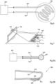
- Figure 2 illustrates apparatus 200 for forming a graphene device such as the device of Figure 1 according to an example embodiment.
- the step of forming the graphene film 100 for example involves forming mono-layers of graphene using the apparatus 200.
- a similar apparatus is described in the publication entitled “ Homogeneous Optical and Electronic Properties of Graphene Due to the Suppression of Multilayer Patches During CVD on Copper Foils", Z. Han et al., Adv. Funct. Mater., 2013, DOI: 10.1002/adfm.201301732 , the contents of which is hereby incorporated by reference.
- the apparatus 200 comprises a reaction chamber 202 in which the graphene film is formed.
- the reaction chamber 202 is a tube furnace or other type of chamber that can be heated.
- a substrate 204 for example formed of a copper foil having a thickness of between 0.1 and 100 ⁇ m, is placed within the chamber 202.
- the substrate 204 provides a surface suitable for graphene formation.
- the material of the substrate 204 is for example selected as one that provides a catalyst for graphene formation, and for example has relatively low carbon solubility.
- other possible materials for forming the substrate 204 include other metals such as nickel, cobalt, or ruthenium or copper alloys such as alloys of copper and nickel, copper and cobalt, copper and ruthenium, or dielectric materials, such as zirconium dioxide, hafnium oxide, boron nitride and aluminum oxide.
- the substrate 204 could have a 3D form.
- the dimensions of such a substrate 204 could be anywhere from 0.1 ⁇ m to several cm or more.
- the substrate 204 could be formed on a planar or 3D surface of a further substrate, for example of copper or another material such as sapphire.
- An inlet 206 of the reaction chamber 202 allows gases to be introduced into the chamber, and an outlet 208 allows gases to be extracted from the chamber.
- the inlet 206 is for example supplied with gas by three gas reservoirs 210A, 210B and 210C, which in the example of Figure 2 respectively store hydrogen (H2), argon (Ar), and methane (CH4).
- gases could be used.
- a different etching gas in other words one that is reactive with carbon, could be used, such as oxygen.
- argon another inert gas could be used, such as helium. This gas is for example used to control the overall pressure in the reaction chamber 202, and could be omitted entirely in some embodiments.
- a different organic compound gas could be used, such as butane, ethylene or acetylene.
- the inlet 206 is coupled to: reservoir 210A via a tube 212A comprising a valve 214A; reservoir 210B via a tube 212B comprising a valve 214B; and reservoir 210C via a tube 212C comprising a valve 214C.
- the valves 214A to 214C control the flow rates of the respective gases into the chamber.
- the valves 214A to 214C are for example electronically controlled by a computing device 216.
- the computing device 216 for example comprises a processing device 218, under the control of an instruction memory 220 storing program code for controlling at least part of the graphene formation process.
- the outlet 208 is for example coupled via a tube 222 to an evacuation pump 224 for evacuating gases from the reaction chamber 202.
- the rate of evacuation by the pump 224 is for example also controlled by the computing device 216.
- the computing device may also control one or more heating elements of the reaction chamber 202 to heat the interior of the chamber during the graphene formation process.
- a deposition chamber 228 is for example provided for depositing the polymer layer over the graphene film.
- a trapdoor 230 in one wall of the chamber 202 and a passageway 231 between the chambers 202, 228 permit the substrate 204 with graphene film to be transferred between the chambers 202 and 228 without being exposed to the atmosphere.
- the deposition chambers 202 and 228 could be separate from each other, and the substrate 204 with graphene film could be transferred without using a passageway.
- the deposition chamber 228 for example comprises an inlet 232 coupled via a further valve 214D to a supply chamber 234 for providing a precursor for depositing the polymer material to cover the graphene film.
- the valve is for example controlled by the computing device 216.
- the polymer material is for example deposited using gas phase deposition.
- gas phase deposition is considered here to include physical vapor deposition (PVD), chemical vapor deposition (CVD and atomic layer deposition (ALD).
- the precursor is for example heated in the supply chamber 234 to between 100°C and 500°C before being introduced as a vapor phase into the chamber 228 via the valve 214D.
- Figures 3A to 3C are cross-section views of a graphene device during its fabrication, for example using the apparatus of Figure 2 .
- a graphene film 100 has been formed by CVD over a substrate 204, which is for example a copper foil.
- Figure 3B illustrates an operation in which the polymer support is deposited covering the graphene film 100.
- the graphene is deposited over a relatively flat substrate 204, and the polymer material is deposited as a conformal layer 302 of substantially uniform thickness that encapsulates the device, including the substrate 204.
- the device is suspended such that the polymer is deposited on all faces of the device.
- the device could be turned over during the deposition process.
- the polymer material could be deposited only over the graphene film 100.
- the polymer material could be deposited in other forms, as will be described in more detail below.
- Figure 3C illustrates a subsequent operation in which the substrate 204 is removed, for example by an etching step or by delaminating the polymer layer with the graphene film 100 from the substrate 204.
- the etching step involves removing the polymer coating covering the substrate 204, for example using a plasma etch, or by scraping with a sharp blade, in order to expose the surface of the substrate.
- the substrate is then removed, for example using a suitable etch, such as an acid etch or using an electrolysis technique.
- an electrochemical delamination process may be performed as described in more detail in the publication entitled “ Electrochemical delamination of CVD-Grown Graphene Film: Toward the Recyclable Use of Copper Catalyst", Yu Wang et al., the contents of which is hereby incorporated by reference to the extent permitted by the law.
- the present inventors have found that this polymer support 102 not only repairs to some extent any defects in the graphene film 100, but also limits further degradation of the graphene film 100 during the separation of the graphene film 100 from the substrate 204.
- An advantage of the process described herein is that no transfer operation is required, reducing the risk that the properties of the graphene film will be degraded.
- graphene is generally formed using a chemical vapor deposition (CVD) process, wherein graphene is formed over a base substrate such as a copper foil.
- CVD chemical vapor deposition
- a difficulty is that it is relatively difficult to remove the graphene layer from the base substrate without damaging or polluting the graphene layer and/or degrading its conductivity.
- the polymer By depositing a polymer material by gas phase deposition in contact with the graphene film, the polymer can remain attached to the graphene while the substrate is removed, for example by etching or by a delamination process, without a transfer step.
- Figures 4A to 4C are cross-section views showing steps in a method of forming a graphene device comprising a three-dimensional graphene film according to an example embodiment.
- a graphene device comprising a three-dimensional graphene film according to an example embodiment.
- such a device is suitable for being placed on or over a 3D form, such as a human or animal member, or a device or part of a device, and for example provides the function of a sensor, of a protection barrier, or the like.
- Figure 4A illustrates an example of a cross-section of a mold 402 over which the graphene device is to be formed.
- the 3D form of this mold 402 shown in Figure 4A is merely one example used for illustration, and many different forms would be possible, depending on the particular application.
- the mold is formed of a material supporting graphene growth, such as copper.
- Figure 4B illustrates operations in which a graphene film 100 is formed over the mold 402, and a coating of polymer, such as of parylene, is then deposited over the graphene film 100.
- Figure 4C illustrates a subsequent operation in which the mold is removed, for example for example by an etching step or by delaminating the polymer layer with the graphene film 100 from the substrate 204, for example using a delaminating operation as described above.
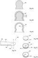
- Figure 5A illustrates a sensing device 500, which in this example is designed to be worn by a user over their index finger or other body part.
- the technique that will be represented in relation to Figure 5A could be applied a variety of different types of sensors having one or more sleeves or tubes adapted to fit around a body part of a human or animal.
- the sensor could be in the form of a glove with a sensor in each finger of the glove in order to detect finger movements.
- the sensor device 500 of Figure 5A comprises a layer of a polymer such as parylene in the form of a sleeve or tube 502 that has dimensions closely fitting an index finger of a user.
- the sleeve 502 is closed at one end to form a finger.
- a film of graphene is formed on a portion of the inside surface of the sleeve 502, and provides an electrode 504 and conductive track 506.
- the electrode 504 is positioned to contact a portion of the underside of a finger near the tip of the finger.
- the electrode 504 is coupled via the conductive track 506 to an end 508 of the sleeve 502 opposite to the fingertip. While not shown in Figure 5A , the end of the conductive track may be coupled via a wire to monitoring equipment, or a monitoring device could be implemented by an integrated circuit mounted on a side of the sleeve 502.
- Figures 5B to 5D are cross-section views of the sensor device 500 of Figure 5A during process steps for forming the sensor device of Figure 5A .
- the cross-sections of Figure 5B to 5D for example correspond to a line A-A shown in Figure 5A , that passes through a portion of the sleeve 502 close to the fingertip and passing through the electrode 504.
- a finger-shaped mold 510 of the same or approximately the same dimensions as the index finger to be used in the sensing device 500 is formed, for example of a material that does not support graphene growth, such as aluminum oxide.
- a thin plating 512 of a material such as copper, which supports graphene growth, is formed in the zone in which the electrode 504 and conductive track 506 are to be formed.
- a first process is for example described in more detail in the publication by J. Zhang et al. entitled “Electron Beam Lithography on Irregular Surfaces Using an Evaporated Resist", ACS Nana 2014, 8(4), pp 3483-3489 , the contents of which is hereby incorporated by reference to the extent permitted by the law.
- an electron or photon sensitive resin is evaporated depending on the type of lithography to be used and on the desired resolution.
- Such a resin can be applied to non-planar surfaces in a desired pattern, followed by a lithography operation.
- a second process is for example described in more detail in the publication by J. Chang et al. entitled “Facile electron-beam lithography technique for irregular and fragile substrates", Applied Physics Letters 105, 173109 (2014 ), the contents of which is hereby incorporated by reference to the extent permitted by the law.
- a resin film is prepared in advance by spin-coating and annealing. After this annealing, the resin film becomes solid and flexible, and can be transferred to the non-planar surface and follows it its 3D form. A lithography step can then be performed.
- the mold is then for example placed in a CVD chamber such as the chamber 202 of the apparatus of Figure 2 , and a graphene film 100 is selectively formed over the plating 512.
- the polymer layer in the form of the sleeve 502 is then formed by coating a layer of polymer over the mold, including over the graphene film 100.
- the polymer coating for example has a thickness of between 50 and 500 ⁇ m. Where this polymer coating contacts the graphene film 100, it provides the polymer support for the graphene film 100.
- polymer sleeve 502, and the graphene film 100 are for example removed from the mold, for example by a delamination process or electrochemical delamination process as described above.
- sensing device 500 comprises a single graphene conductive track 506 leading to a graphene plate forming the electrode 504, many other arrangements would be possible, as will now be described with reference to Figure 6 .
- Figure 6 illustrates the form of a graphene film 100 of the sensing device 500 of Figure 5A according to one example in which two conductive tracks 602, 604 are provided leading to the electrode, and the electrode is implemented in the form of a meandering track electrically connecting the track 602 to the track 604 and formed with a detection zone 606.
- the tracks 602, 604 and the meandering track are for example formed using the lithography or spin-coating process described above with relation to Figure 5B .
- the conductive tracks 602, 604 are for example coupled to a detection circuit 608 for detecting a change in resistance of the conductive track formed in the detection zone.
- the circuit 608 is adapted to apply a substantially constant current through the conductive tracks 602, 604 and to monitor the voltage drop between the conductive tracks 602, 604.
- Pressure applied to the graphene film in the zone 606 for example causes a change in the resistance of the graphene film by deforming the graphene film and/or causing a short circuit between sections of the meandering conductive track. Such a change in the resistance brings about a corresponding change in the voltage across the conductive tracks, which is detection by the detection circuit 608.
- the sensing device of Figure 6 is used in a key stroke detection system, as will now be described in more detail with reference to Figure 7 .
- Figure 7 illustrates a virtual keyboard system in which a projector 702 is provided, in this example mounted on top of a display 704.
- the projector 702 projects an image 706 of a user interface onto a surface.
- the user interface is a keyboard, but in alternative embodiments, other types of user interface can be projected.
- the screen image could be projected in order to provide the functionality of a touch-screen. In such a case, the display 704 could be omitted.
- the system also for example comprises a 3D ranging camera for detecting typing events made by a user on the projected image of the keyboard.
- a 3D ranging camera for detecting typing events made by a user on the projected image of the keyboard.
- a difficulty in such a virtual keyboard system is to confirm a typing event that has been detected visually. For example, a user may move a finger towards a key position with the intention of making a typing stroke, but then pull-back just short of touching the key position. Such a non-completed key stroke may be interpreted as an actual key stroke if based on visual data alone.
- the user for example has one or more sensing devices similar to the ones of Figures 5 and 6 attached to one or more fingers.
- the user wears gloves 708, 710 on their right and left hands respectively, comprising such a sensing device in one, several or all of its fingers.
- Figure 8A is a plan view of a sensing apparatus comprising a pair of graphene films, respectively comprising conductive track 802 and 804.
- the conductive track 802 is connected at one end to a graphene plate 806, while the conductive track 804 is connected at one end to a graphene plate 808.
- the graphene plates 806, 808 are arranged such that they overlap, and they are separated by a deformable insulating layer (not illustrated in Figure 8A ) such that they have an associated capacitance.
- An external compressive force applied to the plates 806, 808, for example caused by a finger hitting a surface will thus change the distance between the plates and cause a change in their capacitance, which can be detected by a detection circuit 809 coupled to the conductive tracks 802, 804.
- Figure 8B is a cross-section view of a sensing device 800 similar to the device 500 of Figure 5A , but adapted to comprise the sensing apparatus of Figure 8A .
- the device 800 for example comprises an outer polymer sleeve 810, having formed therein the plate 808 and the conductive track 804 (not illustrated in Figure 8B ) running along the length of the sleeve. Such a structure is for example formed by the process described with reference to Figures 5B to 5D .
- the device 800 also for example comprises an inner polymer sleeve 812, having formed, on an outer surface thereof, the graphene plate 806, positioned adjacent to the graphene plate 808, and the conductive track 802 (not illustrated in Figure 8B ).
- This structure may also be formed by the method of Figures 5B to 5D , and by then turning the finger inside-out such that the graphene plate 806 is on the outside of the inner polymer sleeve 812.
- the polymer sleeve 812 is then positioned as an inner lining of the polymer sleeve 810 to achieve the structure of Figure 8B .
- the graphene plates 806, 808 are separated by an insulating layer 814 for example formed of polymer, and which may comprise a polymer coating formed over the graphene plate 806 and/or a polymer coating formed over the graphene plate 808.
- the sensing device 800 is placed over a finger or other body part.
- a charge is then for example stored on one of the plates 806, 808 by applying a voltage between the conductive tracks 802, 804, for example by the detection circuit 809.
- the graphene plates 806, 808 then form a detection zone such that if pressure is applied in this zone, the capacitance of the plates 806, 808 will change, causing a change in the voltage on the conductive tracks 802, 804. This voltage change can be detected by the detection circuit 809.
- An advantage of the graphene device described herein is that the polymer layer supports the graphene film 100, helping to maintain relative high conductive properties of the graphene film 100 as it is removed from the mold.
- gas phase deposition allows a thin polymer coating of relatively uniform thickness to be applied that has high conformity with the roughness of the surface of the graphene film, by closely following the contours of the graphene film. In view of its high conformity and uniformity, such a polymer layer exerts a lower stress on the graphene layer than would be possible with other deposition techniques such as spin coating.
- gas phase deposition allows a supporting polymer layer to be realized that strictly conforms to a 3-dimensional shape of the graphene film, both at the nanoscale and at the microscale, respectively helping to preserve the integrity of the film by matching the wrinkles and thereby providing good electrical conductivity and helping to maintain the global 3D shape of the graphene film after the mold removal, allowing depositions on complex shapes such as gloves, etc.
- an advantage of the sensing device described herein is that the polymer coating provides a support layer that remains flexible while holding a graphene electrode in a suitable position for detecting an event such as a key stroke.
Landscapes
- Engineering & Computer Science (AREA)
- Chemical & Material Sciences (AREA)
- General Engineering & Computer Science (AREA)
- Theoretical Computer Science (AREA)
- Organic Chemistry (AREA)
- Power Engineering (AREA)
- Physics & Mathematics (AREA)
- Materials Engineering (AREA)
- Nanotechnology (AREA)
- Microelectronics & Electronic Packaging (AREA)
- Inorganic Chemistry (AREA)
- Human Computer Interaction (AREA)
- General Physics & Mathematics (AREA)
- Life Sciences & Earth Sciences (AREA)
- Manufacturing & Machinery (AREA)
- Health & Medical Sciences (AREA)
- Multimedia (AREA)
- Biophysics (AREA)
- Crystallography & Structural Chemistry (AREA)
- Pathology (AREA)
- Biomedical Technology (AREA)
- Heart & Thoracic Surgery (AREA)
- Medical Informatics (AREA)
- Molecular Biology (AREA)
- Surgery (AREA)
- Animal Behavior & Ethology (AREA)
- General Health & Medical Sciences (AREA)
- Public Health (AREA)
- Veterinary Medicine (AREA)
- Carbon And Carbon Compounds (AREA)
Applications Claiming Priority (3)
| Application Number | Priority Date | Filing Date | Title |
|---|---|---|---|
| FR1551931A FR3033554B1 (fr) | 2015-03-09 | 2015-03-09 | Procede de formation d'un dispositif en graphene |
| PCT/EP2016/054963 WO2016142400A1 (en) | 2015-03-09 | 2016-03-09 | Method of forming a graphene device |
| EP16709366.5A EP3268312B1 (de) | 2015-03-09 | 2016-03-09 | Verfahren zur formung einer graphenvorrichtung |
Related Parent Applications (2)
| Application Number | Title | Priority Date | Filing Date |
|---|---|---|---|
| EP16709366.5A Division-Into EP3268312B1 (de) | 2015-03-09 | 2016-03-09 | Verfahren zur formung einer graphenvorrichtung |
| EP16709366.5A Division EP3268312B1 (de) | 2015-03-09 | 2016-03-09 | Verfahren zur formung einer graphenvorrichtung |
Publications (2)
| Publication Number | Publication Date |
|---|---|
| EP4462234A2 true EP4462234A2 (de) | 2024-11-13 |
| EP4462234A3 EP4462234A3 (de) | 2025-04-09 |
Family
ID=54186033
Family Applications (2)
| Application Number | Title | Priority Date | Filing Date |
|---|---|---|---|
| EP16709366.5A Active EP3268312B1 (de) | 2015-03-09 | 2016-03-09 | Verfahren zur formung einer graphenvorrichtung |
| EP24203158.1A Pending EP4462234A3 (de) | 2015-03-09 | 2016-03-09 | Verfahren zur formung einer graphenvorrichtung |
Family Applications Before (1)
| Application Number | Title | Priority Date | Filing Date |
|---|---|---|---|
| EP16709366.5A Active EP3268312B1 (de) | 2015-03-09 | 2016-03-09 | Verfahren zur formung einer graphenvorrichtung |
Country Status (6)
| Country | Link |
|---|---|
| US (5) | US11577960B2 (de) |
| EP (2) | EP3268312B1 (de) |
| CN (2) | CN120793909A (de) |
| ES (1) | ES3033284T3 (de) |
| FR (1) | FR3033554B1 (de) |
| WO (1) | WO2016142400A1 (de) |
Families Citing this family (10)
| Publication number | Priority date | Publication date | Assignee | Title |
|---|---|---|---|---|
| US12059560B2 (en) | 2015-03-09 | 2024-08-13 | Centre National De La Recherche Scientifique | Method of forming a device comprising graphene |
| FR3033554B1 (fr) | 2015-03-09 | 2020-01-31 | Centre National De La Recherche Scientifique | Procede de formation d'un dispositif en graphene |
| EP3067073A1 (de) | 2015-03-09 | 2016-09-14 | Centre National De La Recherche Scientifique | Verfahren zur herstellung einer medizinischen vorrichtung mit graphen |
| CN108147400B (zh) * | 2018-01-02 | 2021-01-26 | 京东方科技集团股份有限公司 | 一种石墨烯薄膜的转移方法及装置 |
| CN108793146A (zh) * | 2018-07-03 | 2018-11-13 | 中国科学院上海微系统与信息技术研究所 | 一种转移石墨烯的方法 |
| CN109115327B (zh) * | 2018-07-10 | 2021-01-15 | 杭州高烯科技有限公司 | 一种聚合物/金属/石墨烯复合膜及其在声波探测器中的应用 |
| US12262520B2 (en) | 2018-11-30 | 2025-03-25 | The Research Foundation for The State of University New york | Graphene laminate structures |
| CN109399626B (zh) * | 2018-12-20 | 2020-05-08 | 厦门大学 | 一种可控纳米裁剪石墨烯的方法 |
| FR3131076B1 (fr) | 2021-12-22 | 2024-04-19 | Grapheal | Procede de formation d’un dispositif comprenant du graphene |
| GR1010778B (el) * | 2023-07-18 | 2024-10-01 | Ιδρυμα Τεχνολογιας Και Ερευνας/Ινστιτουτο Επιστημων Χημικης Μηχανικης, | Λεπτα και ευκαμπτα νανοσυνθετα θερμαντικα στοιχεια με βαση το γραφενιο χημικης εναποθεσης |
Citations (1)
| Publication number | Priority date | Publication date | Assignee | Title |
|---|---|---|---|---|
| US20140326700A1 (en) | 2013-05-06 | 2014-11-06 | Centre National De La Recherche Scientfique | Process and device for forming a graphene layer |
Family Cites Families (36)
| Publication number | Priority date | Publication date | Assignee | Title |
|---|---|---|---|---|
| GB0228375D0 (en) | 2002-12-05 | 2003-01-08 | Innovation And Entpr Off Of | Wound mapping |
| CN101048055A (zh) * | 2006-03-30 | 2007-10-03 | 通用电气公司 | 先进的受热器和散热器 |
| US9447251B2 (en) * | 2008-07-01 | 2016-09-20 | Vobeck Materials Corp. | Articles having a compositional gradient and methods for their manufacture |
| JP5569769B2 (ja) | 2009-08-31 | 2014-08-13 | 独立行政法人物質・材料研究機構 | グラフェンフィルム製造方法 |
| KR101405463B1 (ko) | 2010-01-15 | 2014-06-27 | 그래핀스퀘어 주식회사 | 기체 및 수분 차단용 그래핀 보호막, 이의 형성 방법 및 그의 용도 |
| EP2582288B1 (de) | 2010-06-18 | 2018-02-28 | The Regents of The University of Michigan | Implantierbare mikrokomponenten-elektroden |
| US9265665B2 (en) | 2010-07-19 | 2016-02-23 | Kci Licensing, Inc. | Inflatable off-loading wound dressing assemblies, systems, and methods |
| EP3686719B1 (de) * | 2010-12-24 | 2024-08-14 | Graphene Square Inc. | Berührungssensor mit graphen zur simultanen detektion eines drucks und einer position |
| CN102881822A (zh) * | 2011-07-13 | 2013-01-16 | 北京大学 | 一种透明柔性阻变存储器及其制备方法 |
| CN102925859A (zh) | 2011-10-23 | 2013-02-13 | 常州碳元科技发展有限公司 | 一种具有保护层结构的碳层材料的制备方法 |
| CN102925860B (zh) * | 2011-10-23 | 2015-07-01 | 碳元科技股份有限公司 | 一种具有保护层结构的碳层材料的制备方法 |
| US9177688B2 (en) * | 2011-11-22 | 2015-11-03 | International Business Machines Corporation | Carbon nanotube-graphene hybrid transparent conductor and field effect transistor |
| US9630183B2 (en) * | 2012-02-01 | 2017-04-25 | Wayne State University | Electrowetting on dielectric using graphene |
| US20140010744A1 (en) | 2012-07-05 | 2014-01-09 | Ford Global Technologies, Llc | System and method for improving operation of an scr |
| KR101450963B1 (ko) * | 2012-07-27 | 2014-10-16 | 율촌화학 주식회사 | 적층 배리어 필름 |
| WO2014066574A1 (en) * | 2012-10-25 | 2014-05-01 | Applied Materials, Inc. | Growing graphene on substrates |
| CN102920452B (zh) * | 2012-11-02 | 2015-02-11 | 上海交通大学 | 基于石墨烯的柔性冠状心电电极及其制备方法 |
| EP2747158A1 (de) * | 2012-12-24 | 2014-06-25 | Université Pierre et Marie Curie (Paris 6) | Biokompatible kohlenstoffbasierte Elektrode, Verwendung davon und Herstellungsverfahren |
| CN105163682B (zh) | 2013-03-15 | 2018-06-01 | 圣犹达医疗用品电生理部门有限公司 | 力传感消融导管 |
| US9310626B2 (en) | 2013-03-15 | 2016-04-12 | Johnson & Johnson Vision Care, Inc. | Ophthalmic devices with organic semiconductor transistors |
| CN104183701A (zh) * | 2013-05-23 | 2014-12-03 | 海洋王照明科技股份有限公司 | 一种柔性透明导电石墨烯薄膜及其制备方法和应用 |
| US9758381B2 (en) * | 2013-08-05 | 2017-09-12 | National University Of Singapore | Method to transfer two dimensional film grown on metal-coated wafer to the wafer itself in a face-to face manner |
| KR101513136B1 (ko) | 2013-10-07 | 2015-04-17 | 한국과학기술연구원 | 그래핀 필름의 제조방법, 그래핀 필름, 및 이를 포함하는 전자 소자 |
| CN103606535B (zh) * | 2013-11-26 | 2016-01-06 | 深圳市华星光电技术有限公司 | 软性显示器组件的制作方法及其制作的软性显示器组件 |
| WO2015105759A1 (en) * | 2014-01-07 | 2015-07-16 | The Trustees Of The University Of Pennsylvania | Graphene-passivated implantable electrodes |
| TWM487718U (zh) | 2014-01-15 | 2014-10-11 | Catz Inc | 導電貼片結構 |
| CN104000624B (zh) | 2014-04-24 | 2016-04-13 | 温州医科大学 | 一种贴于眼表用于眼轴测量的超声探头 |
| US10164220B1 (en) * | 2014-07-24 | 2018-12-25 | Amazon Technologies, Inc. | Graphene-based battery packaging |
| CN104480450A (zh) * | 2014-12-12 | 2015-04-01 | 重庆墨希科技有限公司 | 一种透明导电复合薄膜及其制造方法 |
| US10073522B2 (en) * | 2014-12-12 | 2018-09-11 | Regents Of The University Of Minnesota | Articles of handwear for sensing forces applied to medical devices |
| US12059560B2 (en) | 2015-03-09 | 2024-08-13 | Centre National De La Recherche Scientifique | Method of forming a device comprising graphene |
| FR3033554B1 (fr) | 2015-03-09 | 2020-01-31 | Centre National De La Recherche Scientifique | Procede de formation d'un dispositif en graphene |
| EP3067073A1 (de) | 2015-03-09 | 2016-09-14 | Centre National De La Recherche Scientifique | Verfahren zur herstellung einer medizinischen vorrichtung mit graphen |
| US20170057827A1 (en) | 2015-09-02 | 2017-03-02 | U.S.A. As Represented By The Administrator Of The National Aeronautics And Space Administration | Graphene transparent conductive electrode |
| KR102097814B1 (ko) * | 2016-10-18 | 2020-05-29 | 주식회사 엘지화학 | 고압 균질화 장치 및 이를 이용한 그래핀의 제조방법 |
| CN108793146A (zh) * | 2018-07-03 | 2018-11-13 | 中国科学院上海微系统与信息技术研究所 | 一种转移石墨烯的方法 |
-
2015
- 2015-03-09 FR FR1551931A patent/FR3033554B1/fr active Active
-
2016
- 2016-03-09 ES ES16709366T patent/ES3033284T3/es active Active
- 2016-03-09 US US15/557,039 patent/US11577960B2/en active Active
- 2016-03-09 EP EP16709366.5A patent/EP3268312B1/de active Active
- 2016-03-09 CN CN202511056076.0A patent/CN120793909A/zh active Pending
- 2016-03-09 WO PCT/EP2016/054963 patent/WO2016142400A1/en not_active Ceased
- 2016-03-09 EP EP24203158.1A patent/EP4462234A3/de active Pending
- 2016-03-09 CN CN201680026619.7A patent/CN107667071A/zh active Pending
-
2022
- 2022-12-14 US US18/081,596 patent/US12054392B2/en active Active
-
2024
- 2024-05-02 US US18/652,932 patent/US12358797B2/en active Active
-
2025
- 2025-06-25 US US19/249,262 patent/US20250320125A1/en active Pending
- 2025-06-25 US US19/249,221 patent/US20250320124A1/en active Pending
Patent Citations (1)
| Publication number | Priority date | Publication date | Assignee | Title |
|---|---|---|---|---|
| US20140326700A1 (en) | 2013-05-06 | 2014-11-06 | Centre National De La Recherche Scientfique | Process and device for forming a graphene layer |
Non-Patent Citations (6)
| Title |
|---|
| HUAN DU ET AL.: "A Virtual Keyboard Based on True-3D Optical Ranging", PROCEEDINGS OF THE BRITISH MACHINE VISION CONFERENCE, vol. 1, pages 220 - 229 |
| I. KHRAPACH ET AL.: "Novel Highly Conductive and Transparent Graphene-Based Conductors", ADVANCED MATERIALS, vol. 24, 2012, pages 2844 - 2849, XP002728448, DOI: 10.1002/ADMA.201200489 |
| J. CHANG ET AL.: "Facile electron-beam lithography technique for irregular and fragile substrates", APPLIED PHYSICS LETTERS, vol. 105, 2014, pages 173109, XP012201957, DOI: 10.1063/1.4900505 |
| J. ZHANG ET AL.: "Electron Beam Lithography on Irregular Surfaces Using an Evaporated Resist", ACS NANA, vol. 8, no. 4, 2014, pages 3483 - 3489 |
| YU WANG, ELECTROCHEMICAL DELAMINATION OF CVD-GROWN GRAPHENE FILM: TOWARD THE RECYCLABLE USE OF COPPER CATALYST |
| Z. HAN ET AL.: "Homogeneous Optical and Electronic Properties of Graphene Due to the Suppression of Multilayer Patches During CVD on Copper Foils", ADV. FUNCT. MATER., 2013 |
Also Published As
| Publication number | Publication date |
|---|---|
| US20240279067A1 (en) | 2024-08-22 |
| EP3268312B1 (de) | 2025-05-14 |
| US20250320125A1 (en) | 2025-10-16 |
| EP4462234A3 (de) | 2025-04-09 |
| US20180057361A1 (en) | 2018-03-01 |
| US11577960B2 (en) | 2023-02-14 |
| US12054392B2 (en) | 2024-08-06 |
| US20230183071A1 (en) | 2023-06-15 |
| ES3033284T3 (en) | 2025-08-01 |
| FR3033554B1 (fr) | 2020-01-31 |
| US20250320124A1 (en) | 2025-10-16 |
| CN107667071A (zh) | 2018-02-06 |
| EP3268312C0 (de) | 2025-05-14 |
| FR3033554A1 (fr) | 2016-09-16 |
| WO2016142400A1 (en) | 2016-09-15 |
| EP3268312A1 (de) | 2018-01-17 |
| CN120793909A (zh) | 2025-10-17 |
| US12358797B2 (en) | 2025-07-15 |
Similar Documents
| Publication | Publication Date | Title |
|---|---|---|
| US12358797B2 (en) | Sensor device formed from conductive graphene film | |
| TWI551925B (zh) | A conductive laminate, a transparent conductive laminate having a pattern wiring, and an optical device | |
| US9215797B2 (en) | Transfer sheet provided with transparent conductive film mainly composed of graphene, method for manufacturing same, and transparent conductor | |
| EP3067073A1 (de) | Verfahren zur herstellung einer medizinischen vorrichtung mit graphen | |
| KR101221581B1 (ko) | 그래핀을 포함하는 유연투명전극 기판의 제조방법 및 이에 따라 제조되는 유연투명전극 기판 | |
| EP3013119A1 (de) | Transparente Heizvorrichtung mit Graphen-Film | |
| WO2013176336A1 (ko) | 플라즈마를 이용한 금속 배선이 함몰된 유연 기판의 제조방법 및 이에 따라 제조되는 유연 기판 | |
| CN110243506A (zh) | 一种压阻式压力传感器及其制备方法 | |
| CN104195516B (zh) | 金属掺杂非晶碳压阻传感元件、其制备方法与调控方法 | |
| US11393655B2 (en) | Liquid chip for electron microscope including electrode | |
| CN104089570B (zh) | 一种压阻传感元件及其制备方法 | |
| CN104477894A (zh) | 一种转移石墨烯的方法 | |
| US11749800B2 (en) | High performance stretchable electrode with full area coverage and method for manufacturing the same | |
| US10868121B2 (en) | Method for forming apparatus comprising two dimensional material | |
| KR20140108829A (ko) | 롤투롤 방식을 이용한 그래핀 필름의 분리, 전사 방법 | |
| CN103252936B (zh) | 复合层结构及具有其的触控显示装置 | |
| KR101381240B1 (ko) | 터치 스크린 패널의 제조 방법 및 이에 의하여 제조된 터치 스크린 패널 | |
| US20180170759A1 (en) | Graphene synthesis | |
| KR101706963B1 (ko) | 그래핀 복합 전극의 제조 방법 | |
| CN104538438A (zh) | 石墨烯掺杂材料及其制备方法、电极、像素结构、显示装置 | |
| Sato et al. | Integration of multilayer graphene wires onto tungsten plugs for carbon/metal hybrid interconnects | |
| KR20150106269A (ko) | 그래핀 전사장치 | |
| KR20170000328U (ko) | 기판 상에 재료를 증착하기 위한 증착 장치 | |
| TW201517066A (zh) | 功能性膜之圖案化方法、電子裝置之製造方法及透明導電性薄膜 |
Legal Events
| Date | Code | Title | Description |
|---|---|---|---|
| PUAI | Public reference made under article 153(3) epc to a published international application that has entered the european phase |
Free format text: ORIGINAL CODE: 0009012 |
|
| STAA | Information on the status of an ep patent application or granted ep patent |
Free format text: STATUS: REQUEST FOR EXAMINATION WAS MADE |
|
| 17P | Request for examination filed |
Effective date: 20240927 |
|
| AC | Divisional application: reference to earlier application |
Ref document number: 3268312 Country of ref document: EP Kind code of ref document: P |
|
| AK | Designated contracting states |
Kind code of ref document: A2 Designated state(s): AL AT BE BG CH CY CZ DE DK EE ES FI FR GB GR HR HU IE IS IT LI LT LU LV MC MK MT NL NO PL PT RO RS SE SI SK SM TR |
|
| PUAL | Search report despatched |
Free format text: ORIGINAL CODE: 0009013 |
|
| AK | Designated contracting states |
Kind code of ref document: A3 Designated state(s): AL AT BE BG CH CY CZ DE DK EE ES FI FR GB GR HR HU IE IS IT LI LT LU LV MC MK MT NL NO PL PT RO RS SE SI SK SM TR |
|
| RIC1 | Information provided on ipc code assigned before grant |
Ipc: C01B 32/194 20170101ALI20250304BHEP Ipc: C01B 32/186 20170101ALI20250304BHEP Ipc: H01G 11/32 20130101ALI20250304BHEP Ipc: A61B 5/00 20060101ALI20250304BHEP Ipc: G06F 3/01 20060101AFI20250304BHEP |