EP4459002A1 - Maskierungsspannvorrichtung - Google Patents
Maskierungsspannvorrichtung Download PDFInfo
- Publication number
- EP4459002A1 EP4459002A1 EP22915797.9A EP22915797A EP4459002A1 EP 4459002 A1 EP4459002 A1 EP 4459002A1 EP 22915797 A EP22915797 A EP 22915797A EP 4459002 A1 EP4459002 A1 EP 4459002A1
- Authority
- EP
- European Patent Office
- Prior art keywords
- workpiece
- masking fixture
- eave
- masking
- coating film
- Prior art date
- Legal status (The legal status is an assumption and is not a legal conclusion. Google has not performed a legal analysis and makes no representation as to the accuracy of the status listed.)
- Pending
Links
Images




Classifications
-
- C—CHEMISTRY; METALLURGY
- C23—COATING METALLIC MATERIAL; COATING MATERIAL WITH METALLIC MATERIAL; CHEMICAL SURFACE TREATMENT; DIFFUSION TREATMENT OF METALLIC MATERIAL; COATING BY VACUUM EVAPORATION, BY SPUTTERING, BY ION IMPLANTATION OR BY CHEMICAL VAPOUR DEPOSITION, IN GENERAL; INHIBITING CORROSION OF METALLIC MATERIAL OR INCRUSTATION IN GENERAL
- C23C—COATING METALLIC MATERIAL; COATING MATERIAL WITH METALLIC MATERIAL; SURFACE TREATMENT OF METALLIC MATERIAL BY DIFFUSION INTO THE SURFACE, BY CHEMICAL CONVERSION OR SUBSTITUTION; COATING BY VACUUM EVAPORATION, BY SPUTTERING, BY ION IMPLANTATION OR BY CHEMICAL VAPOUR DEPOSITION, IN GENERAL
- C23C4/00—Coating by spraying the coating material in the molten state, e.g. by flame, plasma or electric discharge
- C23C4/01—Selective coating, e.g. pattern coating, without pre-treatment of the material to be coated
-
- H—ELECTRICITY
- H10—SEMICONDUCTOR DEVICES; ELECTRIC SOLID-STATE DEVICES NOT OTHERWISE PROVIDED FOR
- H10P—GENERIC PROCESSES OR APPARATUS FOR THE MANUFACTURE OR TREATMENT OF DEVICES COVERED BY CLASS H10
- H10P72/00—Handling or holding of wafers, substrates or devices during manufacture or treatment thereof
- H10P72/70—Handling or holding of wafers, substrates or devices during manufacture or treatment thereof for supporting or gripping
-
- B—PERFORMING OPERATIONS; TRANSPORTING
- B05—SPRAYING OR ATOMISING IN GENERAL; APPLYING FLUENT MATERIALS TO SURFACES, IN GENERAL
- B05B—SPRAYING APPARATUS; ATOMISING APPARATUS; NOZZLES
- B05B12/00—Arrangements for controlling delivery; Arrangements for controlling the spray area
- B05B12/16—Arrangements for controlling delivery; Arrangements for controlling the spray area for controlling the spray area
- B05B12/20—Masking elements, i.e. elements defining uncoated areas on an object to be coated
- B05B12/26—Masking elements, i.e. elements defining uncoated areas on an object to be coated for masking cavities
-
- C—CHEMISTRY; METALLURGY
- C23—COATING METALLIC MATERIAL; COATING MATERIAL WITH METALLIC MATERIAL; CHEMICAL SURFACE TREATMENT; DIFFUSION TREATMENT OF METALLIC MATERIAL; COATING BY VACUUM EVAPORATION, BY SPUTTERING, BY ION IMPLANTATION OR BY CHEMICAL VAPOUR DEPOSITION, IN GENERAL; INHIBITING CORROSION OF METALLIC MATERIAL OR INCRUSTATION IN GENERAL
- C23C—COATING METALLIC MATERIAL; COATING MATERIAL WITH METALLIC MATERIAL; SURFACE TREATMENT OF METALLIC MATERIAL BY DIFFUSION INTO THE SURFACE, BY CHEMICAL CONVERSION OR SUBSTITUTION; COATING BY VACUUM EVAPORATION, BY SPUTTERING, BY ION IMPLANTATION OR BY CHEMICAL VAPOUR DEPOSITION, IN GENERAL
- C23C4/00—Coating by spraying the coating material in the molten state, e.g. by flame, plasma or electric discharge
- C23C4/02—Pretreatment of the material to be coated, e.g. for coating on selected surface areas
-
- C—CHEMISTRY; METALLURGY
- C23—COATING METALLIC MATERIAL; COATING MATERIAL WITH METALLIC MATERIAL; CHEMICAL SURFACE TREATMENT; DIFFUSION TREATMENT OF METALLIC MATERIAL; COATING BY VACUUM EVAPORATION, BY SPUTTERING, BY ION IMPLANTATION OR BY CHEMICAL VAPOUR DEPOSITION, IN GENERAL; INHIBITING CORROSION OF METALLIC MATERIAL OR INCRUSTATION IN GENERAL
- C23C—COATING METALLIC MATERIAL; COATING MATERIAL WITH METALLIC MATERIAL; SURFACE TREATMENT OF METALLIC MATERIAL BY DIFFUSION INTO THE SURFACE, BY CHEMICAL CONVERSION OR SUBSTITUTION; COATING BY VACUUM EVAPORATION, BY SPUTTERING, BY ION IMPLANTATION OR BY CHEMICAL VAPOUR DEPOSITION, IN GENERAL
- C23C4/00—Coating by spraying the coating material in the molten state, e.g. by flame, plasma or electric discharge
- C23C4/12—Coating by spraying the coating material in the molten state, e.g. by flame, plasma or electric discharge characterised by the method of spraying
- C23C4/123—Spraying molten metal
Definitions
- the present disclosure relates to a structure of a masking fixture that can be used when spraying a workpiece.
- a technology for spraying a ceramic insulating film onto a metal workpiece (also called “base material” or “component”) in order to provide a high voltage and heat resistance (for example, Patent Literature 1).
- Patent Literature 1 Japanese Unexamined Patent Application Publication No. 2014-013874
- the thermal spray process uses a heat source to melt or soften materials such as metals and ceramics and then injects the molten particles onto a workpiece to form a coating film, so it is difficult to separate the areas where the coating film is deposited from those where the coating film is not deposited. Therefore, it is necessary to mask the areas on the workpiece where the coating film is not to be deposited beforehand. For example, when the workpiece has openings, the openings need to be masked to prevent them from being filled with the coating film.
- using masking tape is time-consuming and it is difficult to precisely adjust the extent of the masking.
- a masking fixture includes an insertion portion fitted into an opening of a workpiece, a covering portion above the insertion portion covering the opening of the workpiece, and an eave portion above the covering portion projecting outwards from an outer edge of the covering portion.
- the eave portion is preferably located higher than a top surface of the workpiece when the insertion portion is fitted into the opening of the workpiece.
- the eave portion may include a protruding portion at an upper side.
- the eave portion may have a cross-sectional taper shape.
- the masking fixture is preferably made of resin.
- the masking fixture which has the eave portion at the upper part and is fixed by inserting it into the opening of the workpiece, simplifies the masking process and improves productivity.
- FIG. 1 shows a structure of a masking fixture 100 according to an embodiment of the present disclosure.
- FIG. 1A shows a plan view of the masking fixture 100 and
- FIG. 1B shows a cross-sectional view corresponding to A-B shown in the plan view.
- the masking fixture 100 shown in FIG. 1A and FIG. 1B is a masking fixture that is attached to a portion where a coating film is not formed when the coating film is formed on the surface of the workpiece by a thermal spray process.
- the masking fixture 100 is an elongated pin-shaped component having a shape in which a plurality of portions with different external diameters are connected along the longitudinal direction in appearance.
- the masking fixture 100 having the external shape shown in FIG. 1A and FIG. 1B can be provided as an integrated molding.
- the masking fixture 100 can be divided into portions named: an insertion portion 102, a covering portion 104 above the insertion portion 102, and an eave portion 106 above the covering portion 104.
- the masking fixture 100 may further include a protruding portion 108 protruding upwards above the eave portion 106.
- the insertion portion 102 is a portion inserted into an opening (not shown) in the workpiece and has the function of fixing the masking fixture 100 to the workpiece.
- the covering portion 104 is a portion that covers the opening and has the function of preventing any coating film to be formed on the opening.
- the eave portion 106 has a function of adjusting a range of film deposition so that the coating film is not deposited thickly on a side of the covering portion 104.
- the protruding portion 108 is disposed for an operator to hold the masking fixture 100 between the fingertips when attaching and removing it from the workpiece.
- FIG. 1A and FIG. 1B show that the insertion portion 102, the covering portion 104 and the eave portion 106 configuring the masking fixture 100 are cylindrical, each having a different external diameter.
- an external diameter D2 of the covering portion 104 is larger than an external diameter D1 of the insertion portion 102
- an external diameter D3 of the eave portion 106 is larger than the external diameter D2 of the covering portion 104.
- An external diameter D4 of the protruding portion 108 is optional and is required to be smaller than the external diameter D3 so as not to impair the function of the eave portion 106.
- a molten or softened material sprayed during thermal spraying is ideally sprayed from a direction that is roughly perpendicular to a surface of the masking fixture.
- the area under the eave portion 106 is shaded and acts to inhibit the deposition of the molten or softened material being sprayed, but the coating film is formed to some extent even in the shaded area of the eave portion 106 due to the presence of a come around.
- a thickness of the coating film formed under the eave portion 106 by the thermal spraying process can be adjusted by a length P1 of the protruding eave portion 106 and a height H1 of the covering portion 104.
- the external diameter D3 of the eave portion 106 has the relationship D3 > D2 compared to the external diameter D2 of the covering portion 104
- the length P1 to which the eave portion 106 protrudes can be freely adjusted by the external diameter D3 of the eave portion 106.
- the height H1 of the covering portion 104 can also be set independently.
- FIG. 1A and FIG. 1B show the shape of the masking fixture 100 having a cylindrical outline and being used for masking circular openings formed in the workpiece. However, when the openings formed in the workpiece are square, the masking fixture may have a prism-shaped outline.
- the masking fixture 100 may be applied to various thermal spray materials. Metals, alloys, cermet, and ceramics are examples of thermal spray materials.
- the thermal spray material is sprayed onto the workpiece, including the area to which the masking fixture 100 is attached.
- the coating film formed on the surface of the workpiece by the thermal spray process is preferably firmly adhered, but it is preferable that the thermal spray material does not adhere to the surface of the masking fixture 100 (it is difficult to adhere) or can be easily removed even if it does adhere to the surface of the masking fixture 100.
- the masking fixture 100 is preferably made of a resin material or at least the surface is coated with a resin material.
- the resin material is preferably a fluoropolymer, for example PTFE (polytetrafluoroethylene), due to its heat resistance and the ease of removing the coating film formed by the thermal spraying process.
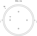
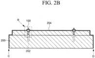
- FIG. 2 shows the masking fixture 100 attached to a workpiece 200.
- FIG. 2A shows a plan view of the workpiece 200 and
- FIG. 2B shows a cross-sectional structure corresponding to C-D shown in the plan view.
- FIG. 2A and FIG. 2B show a case where the workpiece 200 is a substrate stage supporting a semiconductor substrate or a glass substrate in a semiconductor manufacturing apparatus.
- the workpiece 200 is not limited to the shape shown in the figures, and there is no particular limitation in shape as long as the masking fixture 100 is attached to the area where the coating film is formed by the thermal spraying process.
- FIG. 2A shows an example where the masking fixture 100 is attached to four points on the workpiece 200.
- FIG. 2B shows that the workpiece 200 has openings 202.
- the openings 202 have a predetermined depth from the surface of the workpiece 200.
- the masking fixture 100 is inserted into each of the openings 202.
- a coating film 204 is formed on an upper surface and a side surface of the workpiece 200 by the thermal spraying process, the coating film is not formed on the openings 202 due to the masking fixture 100.
- a thickness of the coating film 204 formed by the thermal spraying process is around 100 ⁇ m to 1,500 ⁇ m.
- the masking fixture 100 which is attached to the surface of the workpiece 200, preferably protrudes upwards sufficiently higher than the thickness of the coating film 204, as it becomes difficult to remove the fixture if it is embedded by the coating film 204.
- the masking fixture 100 preferably protrudes at least 1 mm above the surface of the workpiece 200.
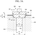
- FIG. 3A shows an enlarged view of the region R shown in FIG. 2B .
- FIG. 3A is a cross-sectional view of the masking fixture 100 attached to the workpiece 200.
- FIG. 3A shows a shape in which an opening groove 203 having a predetermined depth F1 from the upper surface of the workpiece 200 and a diameter K2 wider than a diameter K1 is formed in the upper part of the opening 202 having the diameter K1.
- FIG. 3A shows a shape in which a counterbore having a depth F1 and a diameter K2 is formed at the top of the opening 202 having the diameter K1.
- an upper edge of the aperture groove 203 is preferably counter-bored (shaved) in a tapered shape over a width W1.
- the masking fixture 100 has the insertion portion 102 having the external diameter D1, the covering portion 104 having the external diameter D2 and the eave portion 106 having the external diameter D3.
- the external diameter D1 of the insertion portion 102 and the diameter K1 of the opening 202 are approximately the same diameter, while the external diameter D2 of the covering portion 104 and the diameter K2 of the opening groove 203 are approximately the same diameter.
- the masking fixture 100 can be attached to the workpiece 200 in such a way that the insertion portion 102 is inserted into the opening 202 and the covering portion 104 is fitted into the opening groove 203, so that it cannot easily fall out during the thermal spraying process.
- the masking fixture 100 can then cover (plug) the opening 202 by the masking fixture 100, as the covering portion 104 has an external diameter that is approximately the same as the opening groove 203.
- the eave portion 106 is located higher than the top surface of the workpiece 200 when the masking fixture 100 is attached to the workpiece 200. That is, when the masking fixture 100 is attached to the workpiece 200, the eave portion 106 is arranged to float upwards from the surface of the workpiece 200, rather than in contact with the workpiece 200.
- FIG. 3A shows a situation where a bottom edge of the eave portion 106 is located at a height T1 higher than the top surface of the workpiece 200, due to the height H1 of the covering portion 104 being greater than the depth F1 of the opening groove 203.
- the eave portion 106 is shaped to protrude from the covering portion 104 by the length P1.
- the length P1 of the protruding eave portion 106 may be roughly the same as the width W1 of the tapered portion at the upper end of the opening groove 203.
- the coating film In the area shaded by the eave portion 106, that is, the tapered portion, the coating film is not deposited at all, but the coating film 204 is deposited as the molten or softened material comes around the eave portion 106.
- the coating film 204 deposited on the tapered portion gradually becomes thinner from the area overlapping the outer edge of the eave portion 106 to the inner region. This change in thickness of the coating film 204 is due to a decrease in the amount of molten or softened material going around the eave portion 106 towards the inner side of the eave portion 106.
- the coating film 204 may be stressed and cracks or peeling may occur.
- FIG. 3B shows a tapered shape (reverse tapered shape) in which an upper end portion protrudes outward from a lower end portion in the cross-sectional shape of the eave portion 106.
- the length P1 of the protruding eave portion 106 may be greater than the width W1 of the tapered portion of the opening groove 203. Since the eave portion 106 has a tapered shape, the amount of molten or softened material that can come around can be increased and the thickness of the coating film 204 deposited on the tapered portion of the opening groove 203 can be increased.
- the thickness of the coating film 204 by the shape of the eave portion 106, as the amount of molten or softened material come around can be adjusted by the taper angle of the taper of the eave portion 106 (that is, the amount of come around can be increased when the taper rises close to vertical, and vice versa, and the amount of come around can be reduced).
- FIG. 4 shows an example in which the cross-sectional shape of the end portion of the eave portion 106 is opposite to that of FIG. 3B , and the end portion of the eave portion 106 has a tapered shape (forward tapered shape) such that the lower end portion protrudes outward from the upper end portion.
- a tapered shape forward tapered shape
- the film deposition range and the thickness of the coating film 204 formed by the thermal spraying process on the surface of the workpiece 200 can be adjusted.
- the film deposition range of the coating film 204 can be adjusted by the external shape of the masking fixture 100, so that it can flexibly respond to changes in the size and shape of the openings 202 formed in the workpiece 200.
- the masking fixture 100 can be easily attached and detached by simply inserting it into the opening 202 of the workpiece 200 and pulling it out again, thereby improving productivity.
- the masking fixture 100 is made of resin to prevent the build-up of thermally sprayed coating, and even if it does build-up, the coating can be easily removed so that it can be reused.
Landscapes
- Chemical & Material Sciences (AREA)
- Engineering & Computer Science (AREA)
- Physics & Mathematics (AREA)
- Plasma & Fusion (AREA)
- Chemical Kinetics & Catalysis (AREA)
- Materials Engineering (AREA)
- Mechanical Engineering (AREA)
- Metallurgy (AREA)
- Organic Chemistry (AREA)
- Details Or Accessories Of Spraying Plant Or Apparatus (AREA)
- Coating By Spraying Or Casting (AREA)
- Container, Conveyance, Adherence, Positioning, Of Wafer (AREA)
Applications Claiming Priority (2)
| Application Number | Priority Date | Filing Date | Title |
|---|---|---|---|
| JP2021005010U JP3236603U (ja) | 2021-12-29 | 2021-12-29 | マスキング治具 |
| PCT/JP2022/046646 WO2023127573A1 (ja) | 2021-12-29 | 2022-12-19 | マスキング治具 |
Publications (2)
| Publication Number | Publication Date |
|---|---|
| EP4459002A1 true EP4459002A1 (de) | 2024-11-06 |
| EP4459002A4 EP4459002A4 (de) | 2025-07-30 |
Family
ID=80351942
Family Applications (1)
| Application Number | Title | Priority Date | Filing Date |
|---|---|---|---|
| EP22915797.9A Pending EP4459002A4 (de) | 2021-12-29 | 2022-12-19 | Maskierungsspannvorrichtung |
Country Status (7)
| Country | Link |
|---|---|
| US (1) | US20240342740A1 (de) |
| EP (1) | EP4459002A4 (de) |
| JP (1) | JP3236603U (de) |
| KR (1) | KR20240119288A (de) |
| CN (1) | CN118414448A (de) |
| TW (1) | TWI864527B (de) |
| WO (1) | WO2023127573A1 (de) |
Families Citing this family (2)
| Publication number | Priority date | Publication date | Assignee | Title |
|---|---|---|---|---|
| JP3236293U (ja) * | 2021-12-10 | 2022-02-09 | 日本発條株式会社 | メタルマスク |
| CN116921102A (zh) * | 2022-03-30 | 2023-10-24 | 中国航发商用航空发动机有限责任公司 | 喷涂遮蔽工装件及喷涂方法 |
Family Cites Families (18)
| Publication number | Priority date | Publication date | Assignee | Title |
|---|---|---|---|---|
| JPS5962367A (ja) * | 1982-09-30 | 1984-04-09 | Mazda Motor Corp | マスキング塗装法 |
| JPS59160569A (ja) * | 1983-03-03 | 1984-09-11 | Sumitomo Metal Ind Ltd | 部分溶射方法 |
| JPH0315161Y2 (de) * | 1985-02-01 | 1991-04-03 | ||
| JPS62170169U (de) * | 1986-04-16 | 1987-10-28 | ||
| JPH0525748Y2 (de) * | 1986-08-06 | 1993-06-29 | ||
| JPH0677860U (ja) * | 1993-04-15 | 1994-11-01 | 名古屋油化株式会社 | マスキング材 |
| US6830622B2 (en) * | 2001-03-30 | 2004-12-14 | Lam Research Corporation | Cerium oxide containing ceramic components and coatings in semiconductor processing equipment and methods of manufacture thereof |
| JP2003090229A (ja) * | 2001-09-19 | 2003-03-28 | Amagasaki Tokuzaiken:Kk | ガスタービン尾筒のコーティング方法および詰栓 |
| US20030224198A1 (en) * | 2002-01-11 | 2003-12-04 | Nissan Technical Center North America, Inc. | Reusable masking device for sprayable bed liner |
| DE10392994C5 (de) * | 2002-08-02 | 2013-08-14 | Mitsubishi Heavy Industries, Ltd. | Wärmesperrschicht-Beschichtungsverfahren und dessen Verwendung |
| EP1835045A1 (de) * | 2006-03-15 | 2007-09-19 | Siemens Aktiengesellschaft | Verfahren zur Herstellung eines beschichteten Bauteils |
| WO2011136075A1 (ja) * | 2010-04-28 | 2011-11-03 | 株式会社アルバック | 真空処理装置並びに基板とアラインメントマスクの移動方法及び位置合わせ方法並びに成膜方法 |
| US10276410B2 (en) | 2011-11-25 | 2019-04-30 | Nhk Spring Co., Ltd. | Substrate support device |
| US9259802B2 (en) | 2012-07-26 | 2016-02-16 | Electro Scientific Industries, Inc. | Method and apparatus for collecting material produced by processing workpieces |
| JP6235449B2 (ja) * | 2014-12-03 | 2017-11-22 | 三菱日立パワーシステムズ株式会社 | 溶射皮膜形成方法、タービン用高温部品、タービン、溶射皮膜形成用マスキングピン及びマスキング部材 |
| JP6387889B2 (ja) * | 2015-04-15 | 2018-09-12 | トヨタ自動車株式会社 | 溶射被膜形成方法 |
| US10953424B2 (en) * | 2019-01-03 | 2021-03-23 | The Boeing Company | Flexible three-dimensional maskants |
| KR102936833B1 (ko) * | 2019-03-01 | 2026-03-11 | 닛폰 하츠죠 가부시키가이샤 | 스테이지 및 스테이지 제작 방법 |
-
2021
- 2021-12-29 JP JP2021005010U patent/JP3236603U/ja active Active
-
2022
- 2022-12-19 EP EP22915797.9A patent/EP4459002A4/de active Pending
- 2022-12-19 KR KR1020247022564A patent/KR20240119288A/ko active Pending
- 2022-12-19 CN CN202280084368.3A patent/CN118414448A/zh active Pending
- 2022-12-19 WO PCT/JP2022/046646 patent/WO2023127573A1/ja not_active Ceased
- 2022-12-21 TW TW111149086A patent/TWI864527B/zh active
-
2024
- 2024-06-22 US US18/751,200 patent/US20240342740A1/en active Pending
Also Published As
| Publication number | Publication date |
|---|---|
| WO2023127573A1 (ja) | 2023-07-06 |
| US20240342740A1 (en) | 2024-10-17 |
| CN118414448A (zh) | 2024-07-30 |
| KR20240119288A (ko) | 2024-08-06 |
| TWI864527B (zh) | 2024-12-01 |
| EP4459002A4 (de) | 2025-07-30 |
| JP3236603U (ja) | 2022-03-02 |
| TW202329302A (zh) | 2023-07-16 |
Similar Documents
| Publication | Publication Date | Title |
|---|---|---|
| US20240342740A1 (en) | Masking fixture | |
| KR102311487B1 (ko) | 반도체 패키지의 제조 방법 | |
| CN108914058A (zh) | 一种精密金属掩膜版、蒸镀装置和蒸镀制程 | |
| CN108118290A (zh) | 掩模及其制造方法 | |
| US6189943B1 (en) | Robot hand | |
| KR101727057B1 (ko) | 디스펜싱 지그 | |
| US20160261160A1 (en) | Substrate manufactured from sheet metal and resin, motor provided with substrate, and soldering method therefor | |
| JP6506056B2 (ja) | セラミック部材の製造方法 | |
| EP4446455A1 (de) | Metallmaske | |
| CN108603647A (zh) | 用于机动车照明装置的光模块 | |
| US20160276249A1 (en) | Semiconductor device | |
| TW202223122A (zh) | 金屬遮罩的製造方法 | |
| US20120269599A1 (en) | Threaded structures with solder management features | |
| JP2001323397A (ja) | 薄膜形成装置及びそのコンタクト治具の製造方法 | |
| KR20230173570A (ko) | 정전척 | |
| CN108603274A (zh) | 用于遮盖应以热喷覆层而被覆层的构件的方法 | |
| KR102741639B1 (ko) | 기판 접합체 및 기판 접합 방법 | |
| CN110724928A (zh) | 掩膜板 | |
| CN112575286A (zh) | 金属遮罩 | |
| KR102520177B1 (ko) | 파인메탈마스크 조립체의 제조 방법 | |
| KR20210084135A (ko) | 용액 마스킹 방식에 의한 기재의 코팅 방법 | |
| JP7698554B2 (ja) | 基板の製造方法 | |
| US20140283993A1 (en) | Etching apparatus | |
| CN108990345B (zh) | 壳体及壳体的装饰件安装方法 | |
| KR20160147176A (ko) | 비지에이 반도체 패키지의 전자파 차폐막 형성 방법 및 그 방법에 의해 생산되는 비지에이 반도체 패키지 |
Legal Events
| Date | Code | Title | Description |
|---|---|---|---|
| STAA | Information on the status of an ep patent application or granted ep patent |
Free format text: STATUS: THE INTERNATIONAL PUBLICATION HAS BEEN MADE |
|
| PUAI | Public reference made under article 153(3) epc to a published international application that has entered the european phase |
Free format text: ORIGINAL CODE: 0009012 |
|
| STAA | Information on the status of an ep patent application or granted ep patent |
Free format text: STATUS: REQUEST FOR EXAMINATION WAS MADE |
|
| 17P | Request for examination filed |
Effective date: 20240626 |
|
| AK | Designated contracting states |
Kind code of ref document: A1 Designated state(s): AL AT BE BG CH CY CZ DE DK EE ES FI FR GB GR HR HU IE IS IT LI LT LU LV MC ME MK MT NL NO PL PT RO RS SE SI SK SM TR |
|
| DAV | Request for validation of the european patent (deleted) | ||
| DAX | Request for extension of the european patent (deleted) | ||
| A4 | Supplementary search report drawn up and despatched |
Effective date: 20250701 |
|
| RIC1 | Information provided on ipc code assigned before grant |
Ipc: C23C 4/02 20060101AFI20250625BHEP Ipc: H01L 21/683 20060101ALI20250625BHEP Ipc: B05B 12/26 20180101ALI20250625BHEP |