EP4456161A1 - Prozessanordnung sowie verfahren zur fertigung einer elektrode für eine batteriezelle - Google Patents
Prozessanordnung sowie verfahren zur fertigung einer elektrode für eine batteriezelle Download PDFInfo
- Publication number
- EP4456161A1 EP4456161A1 EP24164169.5A EP24164169A EP4456161A1 EP 4456161 A1 EP4456161 A1 EP 4456161A1 EP 24164169 A EP24164169 A EP 24164169A EP 4456161 A1 EP4456161 A1 EP 4456161A1
- Authority
- EP
- European Patent Office
- Prior art keywords
- measuring
- electrode
- active material
- material layer
- station
- Prior art date
- Legal status (The legal status is an assumption and is not a legal conclusion. Google has not performed a legal analysis and makes no representation as to the accuracy of the status listed.)
- Pending
Links
Images

Classifications
-
- H—ELECTRICITY
- H01—ELECTRIC ELEMENTS
- H01M—PROCESSES OR MEANS, e.g. BATTERIES, FOR THE DIRECT CONVERSION OF CHEMICAL ENERGY INTO ELECTRICAL ENERGY
- H01M4/00—Electrodes
- H01M4/02—Electrodes composed of, or comprising, active material
- H01M4/13—Electrodes for accumulators with non-aqueous electrolyte, e.g. for lithium-accumulators; Processes of manufacture thereof
- H01M4/139—Processes of manufacture
-
- H—ELECTRICITY
- H01—ELECTRIC ELEMENTS
- H01M—PROCESSES OR MEANS, e.g. BATTERIES, FOR THE DIRECT CONVERSION OF CHEMICAL ENERGY INTO ELECTRICAL ENERGY
- H01M4/00—Electrodes
- H01M4/02—Electrodes composed of, or comprising, active material
- H01M4/04—Processes of manufacture in general
- H01M4/0402—Methods of deposition of the material
-
- B—PERFORMING OPERATIONS; TRANSPORTING
- B05—SPRAYING OR ATOMISING IN GENERAL; APPLYING FLUENT MATERIALS TO SURFACES, IN GENERAL
- B05C—APPARATUS FOR APPLYING FLUENT MATERIALS TO SURFACES, IN GENERAL
- B05C9/00—Apparatus or plant for applying liquid or other fluent material to surfaces by means not covered by any preceding group, or in which the means of applying the liquid or other fluent material is not important
- B05C9/08—Apparatus or plant for applying liquid or other fluent material to surfaces by means not covered by any preceding group, or in which the means of applying the liquid or other fluent material is not important for applying liquid or other fluent material and performing an auxiliary operation
- B05C9/12—Apparatus or plant for applying liquid or other fluent material to surfaces by means not covered by any preceding group, or in which the means of applying the liquid or other fluent material is not important for applying liquid or other fluent material and performing an auxiliary operation the auxiliary operation being performed after the application
-
- B—PERFORMING OPERATIONS; TRANSPORTING
- B05—SPRAYING OR ATOMISING IN GENERAL; APPLYING FLUENT MATERIALS TO SURFACES, IN GENERAL
- B05C—APPARATUS FOR APPLYING FLUENT MATERIALS TO SURFACES, IN GENERAL
- B05C9/00—Apparatus or plant for applying liquid or other fluent material to surfaces by means not covered by any preceding group, or in which the means of applying the liquid or other fluent material is not important
- B05C9/08—Apparatus or plant for applying liquid or other fluent material to surfaces by means not covered by any preceding group, or in which the means of applying the liquid or other fluent material is not important for applying liquid or other fluent material and performing an auxiliary operation
- B05C9/14—Apparatus or plant for applying liquid or other fluent material to surfaces by means not covered by any preceding group, or in which the means of applying the liquid or other fluent material is not important for applying liquid or other fluent material and performing an auxiliary operation the auxiliary operation involving heating or cooling
-
- G—PHYSICS
- G01—MEASURING; TESTING
- G01N—INVESTIGATING OR ANALYSING MATERIALS BY DETERMINING THEIR CHEMICAL OR PHYSICAL PROPERTIES
- G01N27/00—Investigating or analysing materials by the use of electric, electrochemical, or magnetic means
- G01N27/02—Investigating or analysing materials by the use of electric, electrochemical, or magnetic means by investigating impedance
- G01N27/04—Investigating or analysing materials by the use of electric, electrochemical, or magnetic means by investigating impedance by investigating resistance
- G01N27/041—Investigating or analysing materials by the use of electric, electrochemical, or magnetic means by investigating impedance by investigating resistance of a solid body
-
- G—PHYSICS
- G01—MEASURING; TESTING
- G01N—INVESTIGATING OR ANALYSING MATERIALS BY DETERMINING THEIR CHEMICAL OR PHYSICAL PROPERTIES
- G01N33/00—Investigating or analysing materials by specific methods not covered by groups G01N1/00 - G01N31/00
- G01N33/0078—Testing material properties on manufactured objects
-
- G—PHYSICS
- G01—MEASURING; TESTING
- G01R—MEASURING ELECTRIC VARIABLES; MEASURING MAGNETIC VARIABLES
- G01R27/00—Arrangements for measuring resistance, reactance, impedance, or electric characteristics derived therefrom
- G01R27/02—Measuring real or complex resistance, reactance, impedance, or other two-pole characteristics derived therefrom, e.g. time constant
- G01R27/08—Measuring resistance by measuring both voltage and current
-
- G—PHYSICS
- G01—MEASURING; TESTING
- G01R—MEASURING ELECTRIC VARIABLES; MEASURING MAGNETIC VARIABLES
- G01R31/00—Arrangements for testing electric properties; Arrangements for locating electric faults; Arrangements for electrical testing characterised by what is being tested not provided for elsewhere
- G01R31/36—Arrangements for testing, measuring or monitoring the electrical condition of accumulators or electric batteries, e.g. capacity or state of charge [SoC]
- G01R31/382—Arrangements for monitoring battery or accumulator variables, e.g. SoC
-
- G—PHYSICS
- G01—MEASURING; TESTING
- G01R—MEASURING ELECTRIC VARIABLES; MEASURING MAGNETIC VARIABLES
- G01R31/00—Arrangements for testing electric properties; Arrangements for locating electric faults; Arrangements for electrical testing characterised by what is being tested not provided for elsewhere
- G01R31/36—Arrangements for testing, measuring or monitoring the electrical condition of accumulators or electric batteries, e.g. capacity or state of charge [SoC]
- G01R31/385—Arrangements for measuring battery or accumulator variables
- G01R31/3865—Arrangements for measuring battery or accumulator variables related to manufacture, e.g. testing after manufacture
-
- H—ELECTRICITY
- H01—ELECTRIC ELEMENTS
- H01M—PROCESSES OR MEANS, e.g. BATTERIES, FOR THE DIRECT CONVERSION OF CHEMICAL ENERGY INTO ELECTRICAL ENERGY
- H01M10/00—Secondary cells; Manufacture thereof
- H01M10/05—Accumulators with non-aqueous electrolyte
- H01M10/052—Li-accumulators
- H01M10/0525—Rocking-chair batteries, i.e. batteries with lithium insertion or intercalation in both electrodes; Lithium-ion batteries
-
- H—ELECTRICITY
- H01—ELECTRIC ELEMENTS
- H01M—PROCESSES OR MEANS, e.g. BATTERIES, FOR THE DIRECT CONVERSION OF CHEMICAL ENERGY INTO ELECTRICAL ENERGY
- H01M10/00—Secondary cells; Manufacture thereof
- H01M10/42—Methods or arrangements for servicing or maintenance of secondary cells or secondary half-cells
- H01M10/4285—Testing apparatus
-
- H—ELECTRICITY
- H01—ELECTRIC ELEMENTS
- H01M—PROCESSES OR MEANS, e.g. BATTERIES, FOR THE DIRECT CONVERSION OF CHEMICAL ENERGY INTO ELECTRICAL ENERGY
- H01M4/00—Electrodes
- H01M4/02—Electrodes composed of, or comprising, active material
- H01M4/04—Processes of manufacture in general
-
- H—ELECTRICITY
- H01—ELECTRIC ELEMENTS
- H01M—PROCESSES OR MEANS, e.g. BATTERIES, FOR THE DIRECT CONVERSION OF CHEMICAL ENERGY INTO ELECTRICAL ENERGY
- H01M4/00—Electrodes
- H01M4/02—Electrodes composed of, or comprising, active material
- H01M4/04—Processes of manufacture in general
- H01M4/0402—Methods of deposition of the material
- H01M4/0404—Methods of deposition of the material by coating on electrode collectors
-
- H—ELECTRICITY
- H01—ELECTRIC ELEMENTS
- H01M—PROCESSES OR MEANS, e.g. BATTERIES, FOR THE DIRECT CONVERSION OF CHEMICAL ENERGY INTO ELECTRICAL ENERGY
- H01M4/00—Electrodes
- H01M4/02—Electrodes composed of, or comprising, active material
- H01M4/04—Processes of manufacture in general
- H01M4/043—Processes of manufacture in general involving compressing or compaction
- H01M4/0435—Rolling or calendering
-
- Y—GENERAL TAGGING OF NEW TECHNOLOGICAL DEVELOPMENTS; GENERAL TAGGING OF CROSS-SECTIONAL TECHNOLOGIES SPANNING OVER SEVERAL SECTIONS OF THE IPC; TECHNICAL SUBJECTS COVERED BY FORMER USPC CROSS-REFERENCE ART COLLECTIONS [XRACs] AND DIGESTS
- Y02—TECHNOLOGIES OR APPLICATIONS FOR MITIGATION OR ADAPTATION AGAINST CLIMATE CHANGE
- Y02E—REDUCTION OF GREENHOUSE GAS [GHG] EMISSIONS, RELATED TO ENERGY GENERATION, TRANSMISSION OR DISTRIBUTION
- Y02E60/00—Enabling technologies; Technologies with a potential or indirect contribution to GHG emissions mitigation
- Y02E60/10—Energy storage using batteries
Definitions
- the invention relates to a process arrangement for producing an electrode for a battery cell according to the preamble of claim 1 and a method for producing such an electrode according to claim 10.
- the electrodes of a lithium-ion battery cell can be manufactured in large-scale production in a continuous process in which a conductor foil is continuously guided as a continuous web through a coating station in which the conductor foil is coated with active material on one or both sides.
- the electrode web thus formed then passes through a drying station in which the active material coated onto the conductor foil is dried. This is followed by a calendering station in which the active material coated onto the conductor foil is compressed to a predefined layer thickness.
- the continuous process ends at a cutting station in which the electrode web is suspended and/or cut to size to form the electrode.
- the electrode thus produced is then integrated into an electrode/separator stack that can be installed in a battery cell.
- the size of the internal resistance of such a battery cell is important for the performance of the battery cell.
- the internal resistance of the battery cell is influenced by, among other things, the specific resistance of the electrode active material and the contact resistance of the active material layer to the conductor foil.
- An analysis device from HIOKO (see brochure "electrode resistance measurement system RM2610 from HIOKO) is known for measuring the specific resistance of the active material layer and the contact resistance, with which the specific resistance and the contact resistance of already finished electrodes can be measured randomly. If the analysis device records an excessively high measurement value for the specific resistance or the contact resistance, all electrodes already manufactured from the entire coating batch of a production interval must be sent to a material scrap and can therefore no longer be used for further battery cell production.
- a method and a device for measuring a coating thickness on a substrate is known.
- the method can also be used specifically to measure the layer thickness of an active material layer on a conductor foil for producing an electrode.
- the object of the invention is to provide a process arrangement and a method for manufacturing an electrode for a battery cell, in which a quality inspection of the electrode can be carried out with less lost material compared to the prior art.
- the invention is based on a process arrangement for producing an electrode for a battery cell.
- a conductor foil is continuously guided as a continuous web through processing stations, specifically to form an electrode web.
- the electrode web is suspended and/or cut to size in a final cutting station to form the electrode.
- a measuring station with a measuring device is integrated in the process arrangement, in which the specific resistance of an active material layer and/or the contact resistance of the active material layer to the conductor foil or a value correlating therewith is measured.
- the measuring process according to the invention does not take place on the finished electrode. Rather, the measuring process takes place directly on the electrode web that has not yet been fed to the cutting station, i.e. before the electrode is finished. In this way, an "in-line" quality check of the specific resistance or the contact resistance between the film and the coating is provided. If quality problems are identified in an electrode web section in the measuring station, this electrode web section is sent to a material reject, while other (perfectly tested) electrode web sections from the same coating batch go through the normal process for manufacturing the electrodes. In this way, the material loss during electrode production can be greatly reduced compared to the prior art.
- the process arrangement can have the following as a processing station: a coating station in which a conductor foil as a continuous web can be coated with active material on one or both sides; a drying station for drying the active material layer coated on the conductor foil; and a calendering station in which the The active material coated with a conductor foil is compressed to a predefined layer thickness.
- the calendering station is directly or indirectly followed by the cutting station, in which the electrode web is cut to form the electrode.
- the measuring station for measuring the specific resistance and/or the contact resistance can preferably be arranged immediately before or after the calendering station. Depending on requirements, the specific resistance and the contact resistance can therefore be recorded at an early stage of the process, preferably before the electrode web passes through the calendering station.
- the measuring station integrated into the process arrangement can have an evaluation unit in which a resistance measurement value recorded by the measuring device is compared with a target value stored in the evaluation unit. If there is a significant deviation from the currently recorded resistance measurement value, a currently measured electrode track section can be separated from the regular electrode production and sent to a material scrap, while the other electrode track sections with a perfect resistance measurement value are used for further battery cell production.
- the measuring device can be designed in the manner of an analysis device from HIOKI (see brochure "electrode resistance measurement system RM2610 from HIOKO).
- the measuring device can have at least one micro-electrode array, the electrodes of which are in non-destructive contact with the surface of the active material layer of the electrode track during the measurement.
- the micro-electrode array can be divided into a voltage measuring array and a current measuring array. The voltage measurement and the current measurement can therefore be carried out separately. With the help of the micro-electrode array, a section of the electrode track can therefore be subjected to a predefined current flow at multiple points.
- the resulting potential distribution can be recorded with the help of the electrodes of the voltage measuring array at multiple measuring points on the surface of the active material layer.
- the current is not only conducted through the conductor foil, but also through the active material layer, so that both the contact resistance and the specific resistance can be measured.
- a calculation unit can be assigned to the micro-electrode array. Data from the measured current flow and the measured potential distribution, the layer thickness of the active material layer and the specific resistance of the conductor foil are fed into the calculation unit. In the calculation unit, on the basis of A FEM simulation is carried out on the basis of this data, which is used to determine the specific resistance and the contact resistance of the currently measured electrode track section.
- the measuring station can have a roller arrangement with at least one measuring roller.
- the electrode track runs over the measuring roller.
- the measuring device can be arranged directly on the outer circumference of the measuring roller, which enables a technically simple "in-line” quality inspection.
- the measuring device cannot be arranged directly on a rigid base body of the measuring roller, but rather on the base material of the measuring roller with an elastically flexible buffer material in between.
- the buffer material acts like an overload protection spring, so that the measuring device always presses against the active material layer of the endless web with a predefined pressure force that is determined by the spring constant of the elastically flexible buffer material.
- the measuring process can be carried out reliably regardless of tolerance deviations in the layer thickness of the active material layer.
- the outer circumference of the measuring roller can be covered with an abrasion-resistant coating outside the measuring device. In this way, roller material abrasion can be avoided, which would lead to contamination of the active material layer.
- the roller arrangement has two measuring rollers over which the electrode track runs with both sides. In this case, one side of the electrode track can be brought into measuring contact with the first measuring roller, while the other side of the electrode track can be brought into measuring contact with the second measuring roller.
- the specific resistance ⁇ of the active material layer 3 and the contact resistance ⁇ of the active material layer 3 to the conductor foil 1 can be measured.
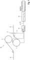
- the core of the invention is that the measuring station M is integrated in the process arrangement for continuous electrode production. This means that the measuring process can be carried out "in line", i.e. during the continuous production process directly on the electrode track E, i.e. at a process point before the electrode is finished.
- the measuring station M has a roller arrangement consisting of two measuring rollers 5, 7, over which the electrode track E runs with its two sides.
- the measuring rollers 5, 7 have the measuring devices 4, which are positioned circumferentially distributed on the outer circumference of each of the measuring rollers 5, 7.
- Current-carrying contacts of the measuring devices 4 can be integrated into the respective measuring roller 5, 7, for example, by means of a cable or by means of a battery solution.
- the two measuring rollers 5, 7 are in the Figure 1 a precision thickness measurement 17 is connected downstream, by means of which a local thickness of the electrode track E is detected.
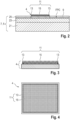
- a measuring device 4 is shown in detail.
- This is realized as a chip with electrode array 11, which is in the Figures 2 to 4 is shown schematically to the extent that it is necessary for understanding the invention.
- the total width of the chip 4 is of the order of magnitude of the coating thickness.
- the chip 4 is according to the Figure 2 Component of a flexible printed circuit board (FPC) design, which consists of a thin, flexible plastic substrate 9 on which electrical conductor tracks and the chip 4 are applied.
- the chip 4 has a micro-electrode array 11, which is divided into a current measuring array 13 and a voltage measuring array 15.
- the current measuring array 13 consists of outer current measuring electrodes on the edge, while the voltage measuring array 15 consists of inner voltage measuring electrodes that are surrounded by the outer current measuring electrodes.
- the current measurement and the voltage measurement are therefore carried out independently of one another by means of the current measuring array 13 and the voltage measuring array 15.
- the electrodes of the micro-electrode array 11 are in non-destructive contact with the surface of the active material layer 3 of the electrode track E.
- An electrode track section that is currently to be measured is subjected to a predefined current flow I at multiple points using the micro-electrode array 11.
- the resulting potential distribution is recorded at multiple measuring points on the surface of the active material layer 3 by the electrodes of the voltage measuring array 15.
- the electrodes of the outer current measuring array 13 can be used as a current source or sink during the measuring process, while the electrodes of the inner voltage measuring array 15 can be used for voltage measurement.
- Each of the electrodes can have a separately controllable or readable channel (this can also be coded).
- the signal connection of the electrodes of the chip 4 to the evaluation unit 19 can be carried out by wireless (5G, WiFi) or wired, inductive contacts after digital coding of the signals.
- the measuring device 4 is in the Figure 1 a calculation unit 16 is assigned to it, into which the data recorded by the current measuring array 13 and the voltage measuring array 15, the data recorded by a thickness measurement 17 of the electrode track E (i.e. the measured electrode track thickness s) can be read.
- the calculation unit 16 determines the specific resistance ⁇ of the active material layer 3 and the contact resistance ⁇ of the active material layer 3 to the arrester film 1 of the electrode track section currently being measured.
- the calculation unit 16 works by means of a local FEM simulation. Therefore, in the calculation unit 16, a simulation of the active material layers 3 located under the chip 4 takes place with the aid of a simulation model and the layer thickness measurement.
- the determined resistance values ⁇ , ⁇ are fed to an evaluation unit 19, which compares the resistance values ⁇ , ⁇ with corresponding target values ⁇ target , ⁇ target. If there is a significant deviation in the currently recorded resistance measurement values, the currently measured electrode track section is not used for further electrode production, but rather is sent to material scrap. If the current resistance measurement values ⁇ , ⁇ are in the range of the target values ⁇ target , ⁇ target without any major deviation, the currently measured electrode track section is used for further battery cell production.
- a current flow I between current measuring electrodes of the current measuring array 13 is indicated with a dashed line. Accordingly, the current I does not flow exclusively through the arrester foil 1, but also through the active material layer 3, so that both the specific resistance ⁇ of the active material layer 3 and the contact resistance ⁇ of the active material layer 3 to the arrester foil 1 can be measured with great accuracy.
- the material structure of the measuring rollers 5, 7 is shown roughly schematically. Accordingly, the respective measuring roller 5, 7 has a rigid base material 21.
- the flexible printed circuit board design FPC is not arranged directly on the rigid base material 21 of the measuring roller 5, but rather with an intermediate layer of an elastically flexible buffer material 23.
- the buffer material 23 acts like an overload protection spring, by means of which the measuring device 4 (i.e. the chip) always presses against the active material layer 3 of the endless web E with a predefined pressure force, regardless of, for example, tolerance deviations in the layer thickness s of the electrode web E.
- the measuring roller 5 is coated on the outer circumference outside the measuring device 4 with an abrasion-resistant coating 25 (made of, for example, PTFE), thereby preventing operational abrasion of the roller material, which could lead to contamination of the active material layer 3.
- an abrasion-resistant coating 25 made of, for example, PTFE
- the chip 4 can also be applied directly to the measuring roller 5. 7 or embedded in a solid layer.
- the roller structure can also be implemented without an abrasion-resistant layer 25.
- the abrasion-resistant layer 25 can also be implemented from metals, such as chrome, nickel, or ceramic coatings, instead of PTFE.
- Another embodiment is a chip with spring-loaded, individual contacts. This can be ensured by any type of spring. It is important that there is no electrical contact between the various electrodes during operation.
Landscapes
- Chemical & Material Sciences (AREA)
- Engineering & Computer Science (AREA)
- Chemical Kinetics & Catalysis (AREA)
- Electrochemistry (AREA)
- Manufacturing & Machinery (AREA)
- General Chemical & Material Sciences (AREA)
- Physics & Mathematics (AREA)
- General Physics & Mathematics (AREA)
- Health & Medical Sciences (AREA)
- Life Sciences & Earth Sciences (AREA)
- Biochemistry (AREA)
- General Health & Medical Sciences (AREA)
- Analytical Chemistry (AREA)
- Immunology (AREA)
- Pathology (AREA)
- Materials Engineering (AREA)
- Food Science & Technology (AREA)
- Medicinal Chemistry (AREA)
- Battery Electrode And Active Subsutance (AREA)
- Fixed Capacitors And Capacitor Manufacturing Machines (AREA)
- Secondary Cells (AREA)
- Investigating Or Analyzing Materials By The Use Of Electric Means (AREA)
Abstract
Die Erfindung betrifft eine Prozessanordnung zur Fertigung einer Elektrode für eine Batteriezelle, in der eine Ableiter Folie (1) als Endlosbahn kontinuierlich durch Bearbeitungsstationen führbar ist, und zwar unter Bildung einer Elektrodenbahn (E), die an einer abschließenden Schneidstation zur Elektrode abgehängt und/oder zugeschnitten wird. Erfindungsgemäß weist die Prozessanordnung eine Messstation (M) mit zumindest einer Messeinrichtung (4) auf, in der der spezifische Widerstand (ρ) einer Aktivmaterial-Schicht (3) und/oder der Übergangswiderstand (Ω) der Aktivmaterial-Schicht (3) zur Ableiter Folie (1) oder ein damit korrelierender Wert messbar ist.
Description
- Die Erfindung betrifft eine Prozessanordnung zur Fertigung einer Elektrode für eine Batteriezelle nach dem Oberbegriff des Anspruches 1 sowie ein Verfahren zur Fertigung einer solchen Elektrode nach Anspruch 10.
- Die Elektroden einer Lithium-lonen-Batteriezelle sind in einer Großserienfertigung in einem kontinuierlichen Prozess fertigbar, bei dem eine Ableiterfolie als Endlosbahn kontinuierlich durch eine Beschichtungsstation geführt wird, in der die Ableiterfolie ein- oder beidseitig mit Aktivmaterial beschichtet wird. Die so gebildete Elektrodenbahn durchläuft anschließend eine Trockenstation, in der das auf die Ableiterfolie beschichtete Aktivmaterial getrocknet wird. Danach folgt eine Kalandrierstation, in der das auf die Ableiterfolie beschichtete Aktivmaterial bis auf eine vordefinierte Schichtdicke verdichtet wird. Der kontinuierliche Prozess endet an einer Schneidstation, in der die Elektrodenbahn zur Elektrode abgehängt und/oder zugeschnitten wird. Die so hergestellte Elektrode wird anschließend in einen Elektroden-/Separatorstapel integriert, der in eine Batteriezelle verbaubar ist.
- Die Größe des Innenwiderstands einer solchen Batteriezelle ist von Bedeutung für die Leistungsfähigkeit der Batteriezelle. Der Batteriezellen-Innenwiderstand wird unter anderem durch den spezifischen Widerstand des Elektroden-Aktivmaterials und durch den Übergangswiderstand der Aktivmaterial-Schicht zur Ableiter Folie mitgeprägt. Zur Messung des spezifischen Widerstands der Aktivmaterial-Schicht sowie des Übergangswiderstands ist ein Analysegerät der Firma HIOKO (siehe Prospekt "electrode resistance measurement system RM2610 der Firma HIOKO) bekannt, mit dem der spezifische Widerstand sowie der Übergangswiderstand bereits fertiggestellter Elektroden stichprobenartig messbar sind. Sofern das Analysegerät einen übermäßig hohen Messwert für den spezifischen Widerstand oder den Übergangswiderstand erfasst, müssen sämtliche bereits gefertigten Elektroden aus der gesamten Beschichtungscharge eines Produktions-Intervalls einem Materialausschuss zugeführt werden und sind diese daher nicht mehr für die weitere Batteriezellen-Fertigung einsetzbar.
- Aus der
DE 10 2014 006 870 A1 ist ein Verfahren sowie eine Vorrichtung zur Messung einer Beschichtungsstärke auf einem Substrat bekannt. Das Verfahren kann speziell auch zur Messung der Schichtdicke einer Aktivmaterial-Schicht auf einer Ableiterfolie zur Herstellung einer Elektrode eingesetzt werden. - Die Aufgabe der Erfindung besteht darin, eine Prozessanordnung sowie ein Verfahren zur Fertigung einer Elektrode für eine Batteriezelle bereitzustellen, in dem eine Qualitätsprüfung der Elektrode mit im Vergleich zum Stand der Technik weniger Verlustmaterial durchführbar ist.
- Die Aufgabe ist durch die Merkmale des Anspruches 1 oder des Anspruches 10 gelöst. Bevorzugte Weiterbildungen der Erfindung sind in den Unteransprüchen offenbart.
- Die Erfindung geht von einer Prozessanordnung zur Fertigung einer Elektrode für eine Batteriezelle aus. In dem Fertigungsprozess wird eine Ableiterfolie als Endlosbahn kontinuierlich durch Bearbeitungsstationen geführt, und zwar unter Bildung einer Elektrodenbahn. Die Elektrodenbahn wird in einer abschließenden Schneidstation zur Elektrode abgehängt und/oder zugeschnitten. Gemäß dem kennzeichnenden Teil des Anspruches 1 ist in der Prozessanordnung eine Messstation mit einer Messeinrichtung integriert, in der der spezifische Widerstand einer Aktivmaterial-Schicht und/oder der Übergangswiderstand der Aktivmaterial-Schicht zur Ableiter Folie bzw. ein damit korrelierender Wert gemessen wird.
- Der erfindungsgemäße Messvorgang findet im Gegensatz zum Stand der Technik nicht erst an der fertiggestellten Elektrode statt. Vielmehr erfolgt der Messvorgang bereits unmittelbar an der noch nicht der Schneidstation zugeführten Elektrodenbahn, das heißt noch vor Fertigstellung der Elektrode. Auf diese Weise ist eine "in-line"-Qualitätsprüfung des spezifischen Widerstands bzw. des Übergangswiderstands zwischen Folie und Beschichtung bereitgestellt. Werden in der Messstation Qualitätsprobleme in einem Elektrodenbahn-Abschnitt erkannt, so wird dieser Elektrodenbahn-Abschnitt einem Materialausschuss zugeführt, während andere (einwandfrei geprüfte) Elektrodenbahn-Abschnitte derselben Beschichtungscharge den normalen Prozess zur Fertigung der Elektroden durchlaufen. Auf diese Weise kann das Verlustmaterial bei der Elektrodenherstellung im Vergleich zum Stand der Technik in hohem Maße reduziert werden.
- In einer technischen Umsetzung kann die Prozessanordnung als Bearbeitungsstation folgendes aufweisen: eine Beschichtungsstation, in der eine Ableiterfolie als Endlosbahn ein- oder beidseitig mit Aktivmaterial beschichtbar ist; eine Trockenstation zum Trocknen des auf die Ableiter Folie beschichtete Aktivmaterial-Schicht; und eine Kalandrierstation in der das auf die Ableiterfolie beschichtete Aktivmaterial bis auf eine vordefinierte Schichtdicke verdichtet wird. Der Kalandrierstation ist mittelbar oder unmittelbar die Schneidstation nachgeschaltet, in der die Elektrodenbahn zur Elektrode abgehängt wird.
- Die Messstation zur Messung des spezifischen Widerstands und/oder des Übergangswiderstand kann bevorzugt unmittelbar vor oder nach der Kalandrierstation angeordnet werden. Je nach Bedarf kann daher der spezifische Widerstand sowie der Übergangswiderstands bereits zu einem frühen Prozesszeitpunkt erfasst werden, und zwar bevorzugt schon bevor die Elektrodenbahn die Kalandrierstation durchläuft.
- Die in der Prozessanordnung eingebundene Messstation kann eine Auswerteeinheit aufweisen, in der ein von der Messeinrichtung erfasster Widerstands-Messwert mit einem in der Auswerteeinheit hinterlegten Sollwert verglichen wird. Bei einer signifikanten Abweichung des aktuell erfassten Widerstands-Messwerts kann ein aktuell vermessener Elektrodenbahn-Abschnitt aus der regulären Elektrodenfertigung ausgegliedert und einem Materialausschuss zugeführt werden, während die anderen Elektrodenbahn-Abschnitte mit einwandfreiem Widerstands-Messwert für die weitere Batteriezellenfertigung eingesetzt werden.
- Die Messeinrichtung kann nach Art eines Analysegeräts der Firma HIOKI (siehe Prospekt "electrode resistance measurement system RM2610 der Firma HIOKO) realisiert sein. In diesem Fall kann die Messeinrichtung zumindest ein Mikro-Elektroden-Array aufweisen, dessen Elektroden während der Messung in zerstörungsfreiem Kontakt mit der Oberfläche der Aktivmaterial-Schicht der Elektrodenbahn sind. Das Mikro-Elektroden-Array kann unterteilt sein in ein Spannungsmess-Array sowie in ein Strommess-Array. Die Spannungsmessung sowie die Strommessung können daher voneinander getrennt durchgeführt werden. Mit Hilfe des Mikro-Elektroden-Arrays kann daher ein Elektrodenbahn-Abschnitt an multiplen Punkten mit einem vordefinierten Stromfluss beaufschlagt werden. Die daraus resultierende Potentialverteilung kann mit Hilfe der Elektroden des Spannungsmess-Arrays an multiplen Messpunkten auf der Oberfläche der Aktivmaterial-Schicht erfasst werden. Beim Messvorgang wird der Strom nicht ausschließlich durch die Ableiterfolie geleitet, sondern auch durch die Aktivmaterial-Schicht, so dass sowohl der Übergangswiderstand als auch der spezifische Widerstand messbar ist.
- Dem Mikro-Elektroden-Array kann eine Berechnungseinheit zugeordnet sein. In die Berechnungseinheit werden Daten aus dem gemessenen Stromfluss sowie der gemessenen Potential-Verteilung, der Schichtdicke der Aktivmaterial-Schicht sowie des spezifischen Widerstands der Ableiterfolie eingespeist. In der Berechnungseinheit findet auf der Grundlage dieser Daten eine FEM-Simulation statt, anhand der der spezifische Widerstand sowie der Übergangswiderstands des aktuell vermessenen Elektrodenbahn-Abschnittes ermittelt wird.
- In einer konkreten Ausführungsvariante kann die Messstation eine Walzenanordnung mit zumindest einer Messwalze aufweisen. Über die Messwalze verläuft die Elektrodenbahn. Die Messeinrichtung kann in diesem Fall unmittelbar auf dem Außenumfang der Messwalze angeordnet sein, wodurch eine prozesstechnisch einfache "in-line"-Qualitätsprüfung ermöglicht ist.
- Im Hinblick auf eine prozesssichere Qualitätsprüfung kann die Messeinrichtung nicht unmittelbar auf einem starren Grundkörper der Messwalze angeordnet sein, sondern vielmehr unter Zwischenlage eines elastisch nachgiebigen Puffermaterials auf dem Grundmaterial der Messwalze angeordnet sein. Das Puffermaterial wirkt nach Art einer Überlastungsschutz-Feder, so dass die Messeinrichtung stets mit einer vordefinierten Andruckkraft, die von der Federkonstante des elastisch nachgiebigen Puffermaterials bestimmt wird, gegen die Aktivmaterial-Schicht der Endlosbahn drückt. Der Messvorgang kann in diesem Fall betriebssicher unabhängig von Toleranzabweichungen in der Schichtdicke der Aktivmaterial-Schicht durchgeführt werden.
- Der Außenumfang der Messwalze kann außerhalb der Messeinrichtung mit einer abriebsfesten Beschichtung überzogen sein. Auf diese Weise kann ein Walzenmaterial-Abrieb vermieden werden, der zu einer Verunreinigung der Aktivmaterial-Schicht führen würde.
- Zur Steigerung der Messgenauigkeit ist es bevorzugt, wenn die Walzenanordnung zwei Messwalzen aufweist, über die Elektrodenbahn mit ihren beiden Seiten läuft. In diesem Fall kann die eine Seite der Elektrodenbahn in Messkontakt mit der ersten Messwalze gebracht werden, während die andere Seite der Elektrodenbahn in Messkontakt mit der zweiten Messwalze bringbar ist.
- Nachfolgend ist ein Ausführungsbeispiel der Erfindung anhand der beigefügten Figuren beschrieben.
- Es zeigen:
- Figuren 1 bis 5
- unterschiedliche Ansichten, anhand derer eine erfindungsgemäße Messstation der Prozessanordnung veranschaulicht sind.
- Mit Hilfe einer Messeinrichtung 4 der Messstation M kann der spezifische Widerstand ρ der Aktivmaterial-Schicht 3 sowie der Übergangswiderstand Ω der Aktivmaterial-Schicht 3 zur Ableiter Folie 1 gemessen werden. Der Kern der Erfindung besteht darin, dass die Messstation M in der Prozessanordnung zur kontinuierlichen Elektrodenfertigung integriert ist. Dadurch ist der Messvorgang "in line", also während des kontinuierlichen Fertigungsprozesses unmittelbar an der Elektrodenbahn E durchführbar, das heißt schon zu einem Prozesszeitpunkt vor Fertigstellung der Elektrode.
- Wie aus der
Figur 1 weiter hervorgeht, weist die Messstation M eine Walzenanordnung aus zwei Messwalzen 5, 7 auf, über die die Elektrodenbahn E mit ihren beiden Seiten läuft. Das heißt, dass gemäß derFigur 1 die eine Seite der Elektrodenbahn E in Messkontakt mit der ersten Messwalze 5 bringbar ist, während die andere Seite der Elektrodenbahn E in Messkontakt mit der zweiten Messwalze 7 bringbar ist. Die Messwalzen 5, 7 weisen die Messeinrichtungen 4 auf, die umfangsverteilt am Außenumfang jeder der Messwalzen 5, 7 positioniert sind. Stromführende Kontakte der Messeinrichtungen 4 können beispielhaft kabelgebunden oder mittels Batterielösung in die jeweilige Messwalze 5, 7 eingebunden sein. Zudem ist den beiden Messwalzen 5, 7 in derFigur 1 eine Präzisions-Dickenmessung 17 nachgeschaltet, mittels der eine lokale Dicke der Elektrodenbahn E erfasst wird. - Von den Messeinrichtungen 4 ist in den
Figur 2 bis 5 eine Messeinrichtung 4 im Detail dargestellt. Diese ist als ein Chip mit Elektroden-Array 11 realisiert, der in denFiguren 2 bis 4 schematisch insoweit dargestellt ist, als es für das Verständnis der Erfindung erforderlich ist. Die Gesamtbreite des Chips 4 ist in der Größenordnung der Beschichtungsdicke bemessen. Zudem ist der Chip 4 gemäß derFigur 2 Bestandteil eines flexiblen Leiterplatten-Designs (flexible printed circuit) FPC, das aus einem dünnen biegsamen Kunststoffsubstrat 9 besteht, auf dem elektrische Leiterbahnen sowie der Chip 4 aufgebracht sind. Der Chip 4 weist ein Mikro-Elektroden-Array 11 auf, das in ein Strommess-Array 13 sowie in ein Spannungsmess-Array 15 unterteilt ist. Das Strommess-Array 13 besteht aus randseitigen äußeren Strommess-Elektroden, während das Spannungsmess-Array 15 aus inneren Spannungsmess-Elektroden besteht, die von den äußeren Strommess-Elektroden umzogen sind. Die Strommessung sowie die Spannungsmessung erfolgen daher mittels des Strommess-Arrays 13 und des Spannungsmess-Arrays 15 voneinander unabhängig. Während eines Messvorgangs (Figur 5 ) sind die Elektroden des Mikro-Elektroden-Arrays 11 in zerstörungsfreiem Kontakt mit der Oberfläche der Aktivmaterial-Schicht 3 der Elektrodenbahn E. Ein aktuell zu vermessender Elektrodenbahn-Abschnitt wird mit Hilfe des Mikro-Elektroden-Arrays 11 an multiplen Punkten mit einem vordefinierten Stromfluss I beaufschlagt. Die daraus resultierende Potential-Verteilung wird an multiplen Messpunkten auf der Oberfläche der Aktivmaterial-Schicht 3 von den Elektroden des Spannungsmess-Arrays 15 erfasst. - Die Elektroden des äußeren Strommess-Arrays 13 sind während des Messvorgangs wahlweise als Stromquelle oder -senke nutzbar, während die Elektroden des inneren Spannungsmess-Arrays 15 für eine Spannungsmessung nutzbar sind. Dabei kann jede der Elektroden über einen gesondert ansteuerbaren oder auslesbaren Kanal (dieser kann auch kodiert werden) verfügen. Die Signalverbindung der Elektroden des Chips 4 zur Auswerteeinheit 19 kann durch kabellose (5G, Wifi) oder kabelgebundene, induktive Kontakte nach digitaler Codierung der Signale ausgeführt werden.
- Der Messeinrichtung 4 ist in der
Figur 1 eine Berechnungseinheit 16 zugeordnet, in die die von dem Strommess-Array 13 und dem Spannungsmess-Array 15 erfassten Daten, die von einer Dickenmessung 17 der Elektrodenbahn E erfassten Daten (das heißt die gemessene Elektrodenbahn-Dicke s) einlesbar sind. Auf der Grundlage dieser Daten sowie des spezifischen Widerstands der Ableiter Folie 1 ermittelt die Berechnungseinheit 16 den spezifischen Widerstand ρ der Aktivmaterial-Schicht 3 sowie den Übergangswiderstand Ω der Aktivmaterial-Schicht 3 zur Ableiter Folie 1 des aktuell vermessenen Elektrodenbahn-Abschnittes. Die Berechnungseinheit 16 arbeitet mittels einer lokalen FEM-Simulation. Von daher erfolgt in der Berechnungseinheit 16 eine Simulation der unter dem Chip 4 befindlichen Aktivmaterial-Schichten 3 mit Hilfe eines Simulationsmodells und der Schichtdickenmessung. - Die ermittelten Widerstands-Werte ρ, Ω werden einer Auswerteeinheit 19 zugeführt, die die Widerstands-Werte ρ, Ω mit entsprechenden Sollwerten ρsoll, Ωsoll vergleicht. Bei einer signifikanten Abweichung der aktuell erfassten Widerstands-Messwerte wird der aktuell vermessene Elektrodenbahn-Abschnitt nicht für die weitere Elektrodenfertigung verwendet, sondern vielmehr einem Materialausschuss zugeführt. Sofern sich die aktuellen Widerstands-Messwerte ρ, Ω ohne größere Abweichung im Bereich der Sollwerte ρsoll, Ωsoll befinden, wird der aktuell vermessene Elektrodenbahn-Abschnitt für die weitere Batteriezellenfertigung verwendet.
- In der
Figur 5 ist mit gestrichelter Linie ein Stromfluss I zwischen Strommess-Elektroden des Strommess-Arrays 13 angedeutet. Demnach fließt der Strom I nicht ausschließlich durch die Ableiterfolie 1, sondern auch durch die Aktivmaterial-Schicht 3, so dass sowohl der spezifische Widerstand ρ der Aktivmaterial-Schicht 3 als auch der Übergangswiderstand Ω der Aktivmaterial-Schicht 3 zur Ableiter Folie 1 mit großer Genauigkeit messbar ist. - In der
Figur 2 ist grob schematisch der Materialaufbau der Messwalzen 5, 7 gezeigt. Demnach weist die jeweilige Messwalze 5, 7 ein starres Grundmaterial 21 auf. Das flexible Leiterplatten-Design FPC ist nicht unmittelbar, sondern vielmehr unter Zwischenlage eines elastisch nachgiebigen Puffermaterials 23 auf dem starren Grundmaterial 21 der Messwalze 5 angeordnet. Das Puffermaterial 23 wirkt nach Art einer Überlastschutz-Feder, mittels der die Messeinrichtung 4 (das heißt der Chip) stets mit einer vordefinierten Andruckkraft gegen die Aktivmaterial-Schicht 3 der Endlosbahn E drückt, und zwar unabhängig von zum Beispiel Toleranzabweichungen in der Schichtdicke s der Elektrodenbahn E. Zudem ist die Messwalze 5 am Außenumfang außerhalb der Messeinrichtung 4 mit einer abriebsfesten Beschichtung 25 (aus zum Beispiel PTFE) überzogen, wodurch ein betriebsbedingter Walzenmaterial-Abrieb vermieden wird, der zu einer Verunreinigung der Aktivmaterial-Schicht 3 führen könnte. - Alternativ zum gezeigten Ausführungsbeispiel kann der Chip 4 auch zum Beispiel direkt auf die Messwalze 5. 7 aufgebracht oder in eine feste Schicht eingebettet sein. Der Walzenaufbau kann ferner auch ohne abriebsfeste Schicht 25 realisiert werden. Zudem kann die abriebsfeste Schicht 25 - anstelle von PTFE - auch aus Metallen, etwa Chrom, Nickel, oder aus Keramikbeschichtungen realisiert werden. Zudem ist ein weiteres Ausführungsbeispiel ein Chip mit gefederten, einzelnen Kontakten. Dies kann durch eine beliebige Art Feder gewährleistet werden. Wichtig ist, dass es im Betrieb keinen elektrischen Kontakt zwischen den verschiedenen Elektroden gibt.
-
- 1
- Ableiterfolie
- 3
- Aktivmaterial-Schicht
- 4
- Messeinrichtung
- 5, 7
- Messwalzen
- 9
- Kunststoffsubstrat
- 11
- Mikro-Elektroden-Array
- 13
- Strommess-Array
- 15
- Spannungsmess-Array
- 16
- Berechnungseinheit
- 17
- Dickenmessung
- 19
- Auswerteeinheit
- 21
- Walzen-Grundmaterial
- 23
- Puffermaterial
- 25
- abriebsfeste Beschichtung
- E
- Elektrodenbahn
- M
- Messstation
- FPC
- flexibles Leiterplatten-Design
- ρ
- spezifischer Widerstand
- Ω
- Übergangswiderstand
- s
- Schichtdicke der Elektrodenbahn E
- I
- Stromfluss
Claims (9)
- Prozessanordnung zur Fertigung einer Elektrode für eine Batteriezelle, in der eine Ableiterfolie (1) als Endlosbahn kontinuierlich durch Bearbeitungsstationen führbar ist, und zwar unter Bildung einer Elektrodenbahn (E), die an einer abschließenden Schneidstation zur Elektrode abgelängt und/oder zugeschnitten wird, dadurch gekennzeichnet, dass die Prozessanordnung eine Messstation (M) mit zumindest einer Messeinrichtung (4) aufweist, in der der spezifische Widerstand (p) einer Aktivmaterial-Schicht (3) und/oder der Übergangswiderstand (Ω) der Aktivmaterial-Schicht (3) zur Ableiter Folie (1) oder ein damit korrelierender Wert messbar ist, und dass insbesondere der Messvorgang unmittelbar an der Elektrodenbahn (E) (in line), das heißt noch vor der Fertigstellung der Elektrode durchführbar ist.
- Prozessanordnung nach Anspruch 1, dadurch gekennzeichnet, dass die Prozessanordnung als Bearbeitungsstationen aufweist:- eine Beschichtungsstation, in der die Ableiter Folie (1) ein- oder beidseitig mit der Aktivmaterial-Schicht (3) beschichtbar ist,- eine Trockenstation zum Trocknen der auf der Ableiter Folie (1) beschichteten Aktivmaterial-Schicht (3),- eine Kalandrierstation, in der die auf die Ableiter Folie (1) beschichtete Aktivmaterial-Schicht (3) bis auf eine vordefinierte Schichtdicke verdichtbar ist, und dass die Schneidstation der Kalandrierstation prozesstechnisch nachgeschaltet ist.
- Prozessanordnung nach Anspruch 1 oder 2, dadurch gekennzeichnet, dass die Messstation (M) der Kalandrierstation prozesstechnisch unmittelbar vor- und/oder nachgeschaltet ist, so dass der spezifische Widerstand (p) bzw. der Übergangswiderstand (Ω) vor und/oder nach dem Kalandriervorgang messbar ist.
- Prozessanordnung nach Anspruch 1, 2 oder 3, dadurch gekennzeichnet, dass die Messstation (M) eine Auswerteeinheit (19) aufweist, die einen von der Messeinrichtung (4) erfassten Widerstands-Messwert (ρ, Ω) mit einem Sollwert (ρsoll, Ωsoll) vergleicht, und dass insbesondere bei einer signifikanten Abweichung des aktuell erfassten Widerstands-Messwerts (ρ, Ω) der aktuell vermessene Elektrodenbahn-Abschnitt nicht für die Elektrodenfertigung verwendet wird, sondern einem Materialausschuss zugeführt wird.
- Prozessanordnung nach einem der vorhergehenden Ansprüche, dadurch gekennzeichnet, dass die Messeinrichtung (4) zumindest ein Mikro-Elektroden-Array (11) aufweist, dessen Elektroden während der Messung in zerstörungsfreiem Kontakt mit der Oberfläche der Aktivmaterial-Schicht (3) sind.
- Prozessanordnung nach Anspruch 5, dadurch gekennzeichnet, dass mittels des Mikro-Elektroden-Arrays (11) ein Elektrodenbahn-Abschnitt an multiplen Punkten mit einem vordefinierten Stromfluss (I) beaufschlagbar ist, und dass die daraus resultierende Potential-Verteilung an multiplen Messpunkten auf der Oberfläche der Aktivmaterial-Schicht (3) erfassbar ist, und/oder dass das Mikro-Elektroden-Array (11) unterteilt ist in ein Strommess-Array (13), dessen Elektroden als Stromquelle sowie Stromsenke zur Erzeugung des Stromflusses (I) wirken, und in ein Spannungsmess-Array (15), dessen Elektroden die aus dem Stromfluss (I) resultierende Potential-Verteilung messen, und/oder dass insbesondere dem Mikro-Elektroden-Array (11) eine Berechnungseinheit (16) zugeordnet ist, die auf der Grundlage des Stromflusses (I), der erfassten Potential-Verteilung, der Schichtdicke (s) der Aktivmaterial-Schicht (3) und des spezifischen Widerstands der Ableiterfolie (1) den spezifischen Widerstand (p) der Aktivmaterial-Schicht (3) sowie den Übergangswiderstand (Ω) berechnet, und zwar insbesondere mittels einer FEM-Simulation.
- Prozessanordnung nach einem der vorhergehenden Ansprüche, dadurch gekennzeichnet, dass die Messstation (M) eine Walzenanordnung mit zumindest einer Messwalze (5, 7) aufweist, über die die Elektrodenbahn (E) läuft, und dass insbesondere die Messeinrichtung (4) am Außenumfang der Messwalze (5, 7) angeordnet ist, oder dass die Messstation (M) einen mit der Elektrodenbahn (E) bewegungsgekoppelten linear verstellbaren Schlitten aufweist, mittels dem die Messeinrichtung (4) über eine lineare Messstrecke in Messkontakt mit der Elektrodenbahn (E) bringbar ist.
- Prozessanordnung nach Anspruch 7, dadurch gekennzeichnet, dass die Messeinrichtung (4) nicht unmittelbar auf einem starren Grundmaterial (21) der Messwalze (5, 7) angeordnet ist, sondern unter Zwischenlage eines elastisch nachgiebigen Puffermaterials (23) auf dem Grundmaterial (21) der Messwalze (5, 7) angeordnet ist, so dass insbesondere die Messeinrichtung (4) mit einer vordefinierten Andruckkraft gegen die Aktivmaterial-Schicht (3) der Elektrodenbahn (E) drückt, und zwar bevorzugt unabhängig von Toleranzabweichungen in der Schichtdicke der Aktivmaterial-Schicht (3), und dass insbesondere der Außenumfang der Messwalze (5, 7) im Bereich außerhalb der Messeinrichtung (4) mit einer abriebsfesten Beschichtung (25) überzogen ist, um eine Verunreinigung der Aktivmaterial-Schicht (3) durch Walzenmaterial-Abrieb zu vermeiden, und/oder dass die Walzenanordnung zwei Messwalzen (5, 7) aufweist, über die die Elektrodenbahn (E) mit ihren beiden Seiten läuft, so dass die eine Seite der Elektrodenbahn (E) in Messkontakt mit der ersten Messwalze (5) bringbar ist, und die andere Seite der Elektrodenbahn (E) in Messkontakt mit der zweiten Messwalze (7) bringbar ist.
- Verfahren zur Fertigung einer Elektrode in einer Prozessanordnung nach einem der vorhergehenden Ansprüche.
Applications Claiming Priority (1)
| Application Number | Priority Date | Filing Date | Title |
|---|---|---|---|
| DE102023203853.6A DE102023203853A1 (de) | 2023-04-26 | 2023-04-26 | Prozessanordnung sowie Verfahren zur Fertigung einer Elektrode für eine Batteriezelle |
Publications (1)
| Publication Number | Publication Date |
|---|---|
| EP4456161A1 true EP4456161A1 (de) | 2024-10-30 |
Family
ID=90366460
Family Applications (1)
| Application Number | Title | Priority Date | Filing Date |
|---|---|---|---|
| EP24164169.5A Pending EP4456161A1 (de) | 2023-04-26 | 2024-03-18 | Prozessanordnung sowie verfahren zur fertigung einer elektrode für eine batteriezelle |
Country Status (7)
| Country | Link |
|---|---|
| US (1) | US20240363828A1 (de) |
| EP (1) | EP4456161A1 (de) |
| JP (1) | JP7774668B2 (de) |
| KR (1) | KR20240158159A (de) |
| CN (1) | CN118867137A (de) |
| CA (1) | CA3236451A1 (de) |
| DE (1) | DE102023203853A1 (de) |
Citations (7)
| Publication number | Priority date | Publication date | Assignee | Title |
|---|---|---|---|---|
| JP2005249758A (ja) * | 2004-03-08 | 2005-09-15 | Fuji Xerox Co Ltd | シートの抵抗測定装置および方法 |
| US20080199775A1 (en) * | 2007-02-01 | 2008-08-21 | Hideharu Takezawa | Battery, examination method and manufacturing method for negative electrode thereof, and examination apparatus and manufacturing apparatus for negative electrode thereof |
| DE102008053009A1 (de) * | 2008-10-23 | 2010-04-29 | Li-Tec Battery Gmbh | Elektroden für eine nach galvanischen Prinzipien arbeitende elektrische Einrichtung, wie Lithium-Ionen-Zellen, und Verfahren zu deren Herstellung |
| DE102014006870A1 (de) | 2014-05-10 | 2014-11-27 | Daimler Ag | Verfahren und Vorrichtung zur Messung einer Beschichtungsstärke auf einem Substrat |
| JP2017077548A (ja) * | 2015-10-22 | 2017-04-27 | トヨタ自動車株式会社 | 塗布装置 |
| JP2018113110A (ja) * | 2017-01-09 | 2018-07-19 | トヨタ自動車株式会社 | 電池の製造方法 |
| DE102021210784A1 (de) * | 2021-09-28 | 2023-03-30 | Volkswagen Aktiengesellschaft | Verfahren zur Herstellung einer strukturierten Elektrodenlage für eine Lithium-Ionen-Batteriezelle |
Family Cites Families (3)
| Publication number | Priority date | Publication date | Assignee | Title |
|---|---|---|---|---|
| JP5994220B2 (ja) * | 2011-08-04 | 2016-09-21 | 日産自動車株式会社 | 電極シートの検査装置 |
| DE102014101051A1 (de) * | 2014-01-29 | 2015-07-30 | Thyssenkrupp Ag | Verfahren und Vorrichtung zur Herstellung eines Elektrodenstapels |
| JP6210929B2 (ja) * | 2014-04-23 | 2017-10-11 | 日置電機株式会社 | 判定装置および判定方法 |
-
2023
- 2023-04-26 DE DE102023203853.6A patent/DE102023203853A1/de active Pending
-
2024
- 2024-03-18 EP EP24164169.5A patent/EP4456161A1/de active Pending
- 2024-03-29 JP JP2024055530A patent/JP7774668B2/ja active Active
- 2024-04-22 CN CN202410483405.9A patent/CN118867137A/zh active Pending
- 2024-04-23 KR KR1020240053774A patent/KR20240158159A/ko active Pending
- 2024-04-25 CA CA3236451A patent/CA3236451A1/en active Pending
- 2024-04-25 US US18/646,718 patent/US20240363828A1/en active Pending
Patent Citations (7)
| Publication number | Priority date | Publication date | Assignee | Title |
|---|---|---|---|---|
| JP2005249758A (ja) * | 2004-03-08 | 2005-09-15 | Fuji Xerox Co Ltd | シートの抵抗測定装置および方法 |
| US20080199775A1 (en) * | 2007-02-01 | 2008-08-21 | Hideharu Takezawa | Battery, examination method and manufacturing method for negative electrode thereof, and examination apparatus and manufacturing apparatus for negative electrode thereof |
| DE102008053009A1 (de) * | 2008-10-23 | 2010-04-29 | Li-Tec Battery Gmbh | Elektroden für eine nach galvanischen Prinzipien arbeitende elektrische Einrichtung, wie Lithium-Ionen-Zellen, und Verfahren zu deren Herstellung |
| DE102014006870A1 (de) | 2014-05-10 | 2014-11-27 | Daimler Ag | Verfahren und Vorrichtung zur Messung einer Beschichtungsstärke auf einem Substrat |
| JP2017077548A (ja) * | 2015-10-22 | 2017-04-27 | トヨタ自動車株式会社 | 塗布装置 |
| JP2018113110A (ja) * | 2017-01-09 | 2018-07-19 | トヨタ自動車株式会社 | 電池の製造方法 |
| DE102021210784A1 (de) * | 2021-09-28 | 2023-03-30 | Volkswagen Aktiengesellschaft | Verfahren zur Herstellung einer strukturierten Elektrodenlage für eine Lithium-Ionen-Batteriezelle |
Also Published As
| Publication number | Publication date |
|---|---|
| JP2024159533A (ja) | 2024-11-08 |
| CN118867137A (zh) | 2024-10-29 |
| JP7774668B2 (ja) | 2025-11-21 |
| CA3236451A1 (en) | 2025-06-17 |
| DE102023203853A1 (de) | 2024-10-31 |
| US20240363828A1 (en) | 2024-10-31 |
| KR20240158159A (ko) | 2024-11-04 |
Similar Documents
| Publication | Publication Date | Title |
|---|---|---|
| EP3564015B1 (de) | Strukturbauteil sowie system und verfahren zur detektion von beschädigungen | |
| DE102013004679B4 (de) | Vorrichtung und Verfahren zum Bearbeiten von Leiterplatten | |
| EP0508062A1 (de) | Verfahren und Vorrichtung zur Prüfung einer elektrischen Leiteranordnung | |
| EP2431622A1 (de) | Rotierbares Wälzlager | |
| EP3492188B1 (de) | Vorrichtung mit verschleissteil und messeinrichtung für verschleiss | |
| DE102007031299A1 (de) | Bearbeitungsmaschine zum Bearbeiten eines Werkstücks | |
| EP4456161A1 (de) | Prozessanordnung sowie verfahren zur fertigung einer elektrode für eine batteriezelle | |
| DE102016212666A1 (de) | Verfahren zur Herstellung eines Leiterplattenelements und Leiterplattenelement | |
| DE4406674A1 (de) | Verfahren zum Prüfen einer zu prüfenden Elektrodenplatte | |
| WO2004008566A2 (de) | Vorrichtung und zur prüfung einer elektroden-membran-einheit | |
| DE102016001580A1 (de) | Verfahren zum Herstellen einer Membran-Elektroden-Anordnung für eine Brennstoffzelle | |
| DE102022105284B4 (de) | Maschinelle Handhabungsvorrichtung und Verfahren zum Handhaben eines elektrisch leitfähigen Blechwerkstücks sowie maschinelle Anordnung für die Blechbearbeitung | |
| AT513766A2 (de) | Verfahren zur Messung der Materialstärke breiter Folien | |
| EP4270573A2 (de) | Verfahren und vorrichtung zum detektieren einer kante bei der herstellung eines zellstapels | |
| EP3826781B1 (de) | Verfahren und vorrichtung zur ermittlung der seitlichen bandkontur oder der position der bandkanten eines laufenden metallbandes | |
| DE102024100075A1 (de) | Inline-qualitätsprüfung von metallfolien während der produktion | |
| DE102017126303A1 (de) | Fühlerlehre sowie Verfahren zum parallelen Ausrichten der Siegelfläche einer Sonotrode mit der Siegelfläche eines Gegenwerkzeuges | |
| EP1867422A2 (de) | Vorrichtung und Verfahren zur elektrochemischen Bearbeitung von Werkstücken | |
| DE2437673C3 (de) | Vorrichtung zum Prüfen von Innenlagen mehrlagiger Leiterplatten | |
| DE102021105584A1 (de) | Verfahren zur Herstellung einer Markierung, Verfahren zur Herstellung einer Energiespeicherzelle sowie Kraftfahrzeug | |
| DE10003679A1 (de) | Verfahren und Vorrichtungen zum Erfassen von Fehlern der Beschichtung eines Trägermaterials | |
| EP3619541B1 (de) | Vorrichtung und verfahren zur kontaktierung eines elektronischen oder elektrischen systems | |
| DE102024125919A1 (de) | Systeme und verfahren zur inline-überwachung von eigenschaften einer bahn während eines herstellungsverfahrens | |
| DE102020133783A1 (de) | Verfahren und Vorrichtung zur Gütebestimmung einer Sinterpastenschicht | |
| WO1997026780A1 (de) | Leiterplatten-trägervorrichtung |
Legal Events
| Date | Code | Title | Description |
|---|---|---|---|
| PUAI | Public reference made under article 153(3) epc to a published international application that has entered the european phase |
Free format text: ORIGINAL CODE: 0009012 |
|
| STAA | Information on the status of an ep patent application or granted ep patent |
Free format text: STATUS: THE APPLICATION HAS BEEN PUBLISHED |
|
| AK | Designated contracting states |
Kind code of ref document: A1 Designated state(s): AL AT BE BG CH CY CZ DE DK EE ES FI FR GB GR HR HU IE IS IT LI LT LU LV MC ME MK MT NL NO PL PT RO RS SE SI SK SM TR |
|
| STAA | Information on the status of an ep patent application or granted ep patent |
Free format text: STATUS: REQUEST FOR EXAMINATION WAS MADE |
|
| 17P | Request for examination filed |
Effective date: 20250430 |
|
| RAP1 | Party data changed (applicant data changed or rights of an application transferred) |
Owner name: POWERCO SE |