EP4455736A1 - Röntgendetektor - Google Patents
Röntgendetektor Download PDFInfo
- Publication number
- EP4455736A1 EP4455736A1 EP22912024.1A EP22912024A EP4455736A1 EP 4455736 A1 EP4455736 A1 EP 4455736A1 EP 22912024 A EP22912024 A EP 22912024A EP 4455736 A1 EP4455736 A1 EP 4455736A1
- Authority
- EP
- European Patent Office
- Prior art keywords
- circuit unit
- gate
- flexible circuit
- sensor panel
- ray detector
- Prior art date
- Legal status (The legal status is an assumption and is not a legal conclusion. Google has not performed a legal analysis and makes no representation as to the accuracy of the status listed.)
- Pending
Links
Images

Classifications
-
- G—PHYSICS
- G01—MEASURING; TESTING
- G01T—MEASUREMENT OF NUCLEAR OR X-RADIATION
- G01T1/00—Measuring X-radiation, gamma radiation, corpuscular radiation, or cosmic radiation
- G01T1/16—Measuring radiation intensity
- G01T1/20—Measuring radiation intensity with scintillation detectors
- G01T1/2018—Scintillation-photodiode combinations
- G01T1/20188—Auxiliary details, e.g. casings or cooling
-
- G—PHYSICS
- G01—MEASURING; TESTING
- G01T—MEASUREMENT OF NUCLEAR OR X-RADIATION
- G01T1/00—Measuring X-radiation, gamma radiation, corpuscular radiation, or cosmic radiation
- G01T1/16—Measuring radiation intensity
- G01T1/20—Measuring radiation intensity with scintillation detectors
- G01T1/2018—Scintillation-photodiode combinations
- G01T1/20184—Detector read-out circuitry, e.g. for clearing of traps, compensating for traps or compensating for direct hits
-
- G—PHYSICS
- G01—MEASURING; TESTING
- G01T—MEASUREMENT OF NUCLEAR OR X-RADIATION
- G01T1/00—Measuring X-radiation, gamma radiation, corpuscular radiation, or cosmic radiation
- G01T1/16—Measuring radiation intensity
- G01T1/20—Measuring radiation intensity with scintillation detectors
- G01T1/2018—Scintillation-photodiode combinations
- G01T1/20182—Modular detectors, e.g. tiled scintillators or tiled photodiodes
-
- G—PHYSICS
- G01—MEASURING; TESTING
- G01T—MEASUREMENT OF NUCLEAR OR X-RADIATION
- G01T1/00—Measuring X-radiation, gamma radiation, corpuscular radiation, or cosmic radiation
- G01T1/16—Measuring radiation intensity
- G01T1/24—Measuring radiation intensity with semiconductor detectors
- G01T1/244—Auxiliary details, e.g. casings, cooling, damping or insulation against damage by, e.g. heat, pressure or the like
-
- H—ELECTRICITY
- H10—SEMICONDUCTOR DEVICES; ELECTRIC SOLID-STATE DEVICES NOT OTHERWISE PROVIDED FOR
- H10F—INORGANIC SEMICONDUCTOR DEVICES SENSITIVE TO INFRARED RADIATION, LIGHT, ELECTROMAGNETIC RADIATION OF SHORTER WAVELENGTH OR CORPUSCULAR RADIATION
- H10F39/00—Integrated devices, or assemblies of multiple devices, comprising at least one element covered by group H10F30/00, e.g. radiation detectors comprising photodiode arrays
- H10F39/10—Integrated devices
- H10F39/12—Image sensors
- H10F39/18—Complementary metal-oxide-semiconductor [CMOS] image sensors; Photodiode array image sensors
- H10F39/189—X-ray, gamma-ray or corpuscular radiation imagers
-
- H—ELECTRICITY
- H10—SEMICONDUCTOR DEVICES; ELECTRIC SOLID-STATE DEVICES NOT OTHERWISE PROVIDED FOR
- H10F—INORGANIC SEMICONDUCTOR DEVICES SENSITIVE TO INFRARED RADIATION, LIGHT, ELECTROMAGNETIC RADIATION OF SHORTER WAVELENGTH OR CORPUSCULAR RADIATION
- H10F39/00—Integrated devices, or assemblies of multiple devices, comprising at least one element covered by group H10F30/00, e.g. radiation detectors comprising photodiode arrays
- H10F39/10—Integrated devices
- H10F39/12—Image sensors
- H10F39/191—Photoconductor image sensors
- H10F39/195—X-ray, gamma-ray or corpuscular radiation imagers
Definitions
- the present disclosure relates to an X-ray detector.
- An X-ray detector is used for medical or industrial purposes as a digital X-ray image sensor device.
- the X-ray detector includes a sensor panel, gate ICs each mounted on flexible printed circuit boards (FPCBs) each connected to one side of the sensor panel, readout ICs each mounted on another FPCBs each connected to another side adjacent to the one side of the sensor panel, a gate circuit unit such as a PCB electrically connected to the gate ICs, and a readout circuit unit such as yet another PCB electrically connected to the readout ICs.
- FPCBs flexible printed circuit boards
- the X-ray detector In the case of an X-ray detector that is used to detect defects in pipes as the industrial X-ray detector, the X-ray detector needs to be bent to match the round outer appearance of the pipe to prevent image distortion. When the X-ray detector is bent in this way, there may be a problem of damage to at least one of the gate circuit units or read out circuit units.
- the present disclosure has been made keeping in mind the above problems occurring in the related art and aims to provide a way to prevent damage to circuit units even when an X-ray detector is bent.
- a X-ray detector including: a sensor panel having flexible characteristics; at least one first flexible circuit unit configured to be attached along a first edge of the sensor panel and have a gate IC mounted thereon; at least one second flexible circuit unit configured to be attached along a second edge of the sensor panel and have a readout IC mounted thereon; a third flexible circuit unit configured to be attached to one end of the first edge; and a main circuit unit configured to be connected to the third flexible circuit unit and have a timing controller mounted thereon, wherein a gate control signal output from the main circuit unit is provided to the gate IC via the third flexible circuit unit.
- the sensor panel may include a first connection wire connecting the third flexible circuit unit and the first flexible circuit unit.
- the sensor panel may be provided with a plurality of the first flexible circuit units each having the gate IC mounted thereon along the first edge, and the sensor panel may include second connection wires, the wire configured to electrically connect the gate ICs of the first flexible circuit units adjacent to each other.
- the X-ray detector may further include a driving circuit unit configured to be connected between the second flexible circuit unit and the main circuit unit.
- the X-ray detector may further include a first support board with flexible characteristics configured to support a rear side of the sensor panel.
- the X-ray detector may further include a second support board having one surface configured to have the driving circuit unit placed thereon and an opposite surface configured to have the main circuit unit placed thereon.
- the driving circuit unit and the main circuit unit may be located on one side of the second edge so as not to overlap the sensor panel in a planar manner.
- the main circuit unit and the gate ICs are configured to be electrically connected through the third flexible circuit unit so that the gate control signal can be transmitted, thereby allowing a circuit unit of the hard material for driving the gate IC to be eliminated.
- the X-ray detector may be bent without any damage to its components, as there is no separate circuit unit for driving the gate IC present in this direction.
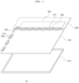
- FIG. 1 is a perspective view schematically showing an X-ray detector according to an embodiment of the present disclosure.
- FIG. 1 some components of the X-ray detector are shown for convenience of explanation.
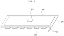
- FIG. 2 is a perspective view schematically showing a main board, a second support board, and second and third flexible circuit units of the X-ray detector according to the embodiment of the present disclosure.
- FIG. 3 is a block diagram schematically showing the X-ray detector according to the embodiment of the present disclosure.
- the X-ray detector 10 may include a sensor panel 100, first flexible circuit units 200 configured to have gate ICs 210 respectively mounted thereon, second flexible circuit units 300 configured to have readout ICs 310 respectively mounted thereon, a third flexible circuit unit 400, a driving circuit unit 350, a main circuit unit 500, a first support board 610, and a second support board 620.
- At least one gate IC 210 may be used, but in the present embodiment, a case in which a plurality of gate ICs 210 and a plurality of first flexible circuit units 200 on which the plurality of gate ICs 210 is respectively mounted is used as an example.
- the first flexible circuit unit may be composed of an FPCB as an example.
- at least one readout IC 310 may be used, but in the present embodiment, a case in which a plurality of readout ICs 310 and a plurality of second flexible circuit units 300 on which the plurality of readout ICs 310 is respectively mounted is used as an example.
- the second flexible circuit unit may be composed of an FPCB as an example.
- the sensor panel 100 generates an electrical signal corresponding to the incident X-rays.
- pixels P which are unit elements that detect X-rays may be disposed in a matrix form.
- the sensor panel 100 may be a direct method that directly converts X-rays into electrical signals or an indirect method that converts X-rays into visible light and then converts them into electrical signals.
- the X-ray detector 10 may further include a phosphor. This phosphor is disposed on the front surface of the sensor panel 100, where X-rays are incident, and may convert the incident X-rays into visible light.
- a plurality of gate wires GL and a plurality of read out wires RL that cross each other may be provided in the sensor panel 100.
- the plurality of gate wires GL may extend, for example, along a first direction (or row direction) and be connected to the pixels P disposed in the corresponding row line.
- gate signals are sequentially applied to the plurality of gate wires GL from the plurality of gate ICs 210, and the gate signals may be transmitted to the pixels P of the corresponding row lines.
- the plurality of read out lines RL may extend, for example, along a second direction (or column direction) and be connected to pixels P disposed in a corresponding column line.
- the read out wires RL may be applied with electrical signals generated from the pixels P of the corresponding column line, respectively, and the electrical signals may be transmitted to the corresponding readout IC 310.
- the sensor panel 100 may be configured to have flexible characteristics.
- a substrate on which the sensor array elements of the sensor panel 100 are provided may be made of a material with flexible characteristics, such as plastic, or thin glass to have flexible characteristics.
- First flexible circuit units 200 with gate ICs 210 respectively mounted thereon may be connected to an edge of one side of the sensor panel 100, for example, a first edge.
- One end of the corresponding gate wire GL is connected to the output terminal of the first flexible circuit unit 200, and the gate signal output from the gate IC 210 mounted on the first flexible circuit unit 200 may be applied to the gate wire GL.
- the second flexible circuit units 300 with flexible characteristics, on which readout IC s 310 are respectively mounted may be connected.
- One end of the corresponding read out wire RL is connected to the output terminal of the second flexible circuit unit 300, and the electrical signal of the pixel transmitted through the read out wire RL may be input to the readout IC 310 that is mounted on the corresponding second flexible circuit unit 300.
- the driving circuit unit 350 corresponds to a circuit unit for driving the readout IC 310 and may be connected to the plurality of second flexible circuit units 300.
- the driving circuit unit 350 may be applied with the electrical signal output from the readout IC 310.
- the driving circuit unit 350 may output a read out control signal to the readout IC 310 to control the operation of the readout IC 310.
- Such a driving circuit unit 350 may be made of a PCB which is a hard material with the characteristic of not being substantially bent.
- the third flexible circuit unit 400 having flexible characteristics may be connected to one end part of the first edge.
- the third flexible circuit unit 400 may be connected to one end part of the first edge located adjacent to the second edge.
- the third flexible circuit unit 400 may be attached to the first edge area between the corner that is located between the first and second edges and the area where the first flexible circuit unit 210 which is closest to the second edge is attached.
- the main circuit unit 500 and the gate ICs 210 may be electrically connected. Accordingly, the gate control signals that control the driving of the gate ICs 210 may be output from the main circuit unit 500 and then transmitted to the gate ICs 210 through the third flexible circuit unit 400.
- the gate control signal is configured to be transmitted through the third flexible circuit unit 400 by electrically connecting the main circuit unit 500 and the gate ICs 210, a circuit unit for driving the gate ICs made of hard material may be eliminated.
- the circuit unit for driving the gate IC is not used, there is no circuit unit present to drive the gate IC that could be damaged when the X-ray detector 10 is bent, bending the sensor panel 100 along the longitudinal direction of the first edge. Accordingly, the X-ray detector 10 may be freely bent in the direction that the gate ICs 210 are attached.
- the electrical connection structure of the third flexible circuit unit 400 and the gate ICs 210 will be examined in more detail.
- the gate IC 210 closest to the third flexible circuit unit 400 is referred to as the first gate IC 210a, and the remaining gate ICs 210 are referred to as the second gate ICs 210b.
- a space between the first flexible circuit unit 200, on which the first gate IC 210a is mounted, and the third flexible circuit unit 400 may be connected through a first connection wire 121 provided on the substrate of the sensor panel 100. Accordingly, the gate control signal output from the third flexible circuit unit 400 may be input to the first flexible circuit unit 200 via the first connection wire 121 and transmitted to the first gate IC 210a.
- a space between the adjacent gate ICs 210 and, more specifically, a space between adjacent first flexible circuit units 200 may be connected through a second connection wire 122 provided on the substrate of the sensor panel 100.
- a space between the first flexible circuit unit 200, on which the first gate IC 210a is mounted, and the adjacent first flexible circuit unit 200, on which the second gate IC 210b is mounted may be connected through the second connection wire 122 provided on the substrate of the sensor panel 100.
- a space between one first flexible circuit unit 200, on which the second gate IC 210b is mounted, and another first flexible circuit unit 200, on which the second gate IC 210b is mounted and which is located at the rear end of, or adjacent to, the one first flexible circuit unit 200, may be connected through the second connection wire 122 provided on the substrate of the sensor panel 100. Accordingly, the gate control signal provided to the first flexible circuit unit 200, on which the first gate IC 210a is mounted, may be transmitted to the second gate IC 210b via the second connection wire 122.
- the main circuit unit 500 is configured to output control signals that control the operation of the sensor panel 100, gate ICs 210, and readout IC s 310 and to also receive electrical signals output from the readout IC s 310.
- a timing controller 510 is mounted on the main circuit unit 500, and the timing controller 510 may generate various control signals including a gate control signal and a read out control signal.
- the gate control signal may be output to the third flexible circuit unit 400 and provided to the gate ICs 210, and the read out control signal may be output to the driving circuit unit 350 and then provided to the readout IC s 310.
- the electrical signal of the pixel output from the readout IC s 310 is provided to the main circuit unit 500 through the driving circuit unit 350 and may be signal processed in the timing controller 510.
- a first support board 610 may be attached to the sensor panel 100.
- the first support board 610 may be made of a material with flexible characteristics.
- the first support board 610 may have the function of supporting and protecting the sensor panel 100.
- the first support board 610 may cover (or shield) a rear surface of the sensor panel 100 and may further cover the side surfaces of the sensor panel 100.
- Such a first support board 610 may be bent together with the sensor panel 100 and may maintain its shape by supporting the sensor panel 100 in a bent state.
- the second support board 620 may have one surface with the driving circuit unit 350 placed thereon and an opposite surface with the main circuit unit 500 placed thereon.
- the driving circuit unit 350 may be attached to a front surface of the second support board 620
- the main circuit unit 500 may be attached to a rear surface of the second support board 620.
- the second support board 620 may be disposed so as not to overlap the sensor panel 100 in a planar manner.
- the driving circuit unit 350 and the main circuit unit 500 may be disposed so as not to overlap the sensor panel 100 in the planar manner.
- the industrial X-ray detector 10 may have in a flat configuration an X-ray detection area, where the sensor panel 100 is located, and a peripheral area, as one side of the X-ray detection area, where a handle is provided, on one side of the second edge of the sensor panel 100.
- the driving circuit unit 350 and the main circuit unit 500 may be disposed in this peripheral area.
- the X-ray detection area when performing an X-ray inspection, may be bent according to the outer appearance of the inspection object, and the peripheral area where the handle is provided may not be bent and may maintain a substantially flat state.
- the bending direction is the longitudinal direction of the first edge of the sensor panel 100 where the gate ICs 210 are disposed, and there is no separate circuit unit for driving the gate IC present in this direction. Accordingly, the X-ray detector 10 may be bent without any damage to its components.
Landscapes
- Health & Medical Sciences (AREA)
- Physics & Mathematics (AREA)
- Life Sciences & Earth Sciences (AREA)
- General Physics & Mathematics (AREA)
- High Energy & Nuclear Physics (AREA)
- Molecular Biology (AREA)
- Spectroscopy & Molecular Physics (AREA)
- Measurement Of Radiation (AREA)
- Toxicology (AREA)
Applications Claiming Priority (2)
| Application Number | Priority Date | Filing Date | Title |
|---|---|---|---|
| KR1020210187564A KR20230097753A (ko) | 2021-12-24 | 2021-12-24 | 엑스선 디텍터 |
| PCT/KR2022/021188 WO2023121391A1 (ko) | 2021-12-24 | 2022-12-23 | 엑스선 디텍터 |
Publications (2)
| Publication Number | Publication Date |
|---|---|
| EP4455736A1 true EP4455736A1 (de) | 2024-10-30 |
| EP4455736A4 EP4455736A4 (de) | 2026-04-22 |
Family
ID=86903177
Family Applications (1)
| Application Number | Title | Priority Date | Filing Date |
|---|---|---|---|
| EP22912024.1A Pending EP4455736A4 (de) | 2021-12-24 | 2022-12-23 | Röntgendetektor |
Country Status (6)
| Country | Link |
|---|---|
| US (1) | US12585033B2 (de) |
| EP (1) | EP4455736A4 (de) |
| JP (1) | JP2025508296A (de) |
| KR (1) | KR20230097753A (de) |
| CN (1) | CN118541623A (de) |
| WO (1) | WO2023121391A1 (de) |
Families Citing this family (1)
| Publication number | Priority date | Publication date | Assignee | Title |
|---|---|---|---|---|
| KR102747067B1 (ko) * | 2022-10-13 | 2024-12-26 | 주식회사 디알텍 | 엑스선 디텍터 |
Family Cites Families (10)
| Publication number | Priority date | Publication date | Assignee | Title |
|---|---|---|---|---|
| JP2006250899A (ja) * | 2005-03-14 | 2006-09-21 | Fuji Photo Film Co Ltd | テープキャリアおよびこれを用いた放射線検出装置 |
| JP2010078415A (ja) | 2008-09-25 | 2010-04-08 | Fujifilm Corp | 放射線検出装置及び放射線画像撮影システム |
| JP2011075327A (ja) * | 2009-09-29 | 2011-04-14 | Fujifilm Corp | 放射線撮影装置 |
| US11061153B2 (en) * | 2016-12-22 | 2021-07-13 | Carestream Health, Inc. | Flexible digital radiography detector |
| JP6869064B2 (ja) * | 2017-03-22 | 2021-05-12 | 富士フイルム株式会社 | 放射線画像撮影装置 |
| KR102846813B1 (ko) * | 2019-12-23 | 2025-08-14 | 한국전기연구원 | 곡면형 적층 구조 섬광체를 갖는 듀얼 방사선 디텍터 |
| KR102782004B1 (ko) * | 2020-02-06 | 2025-03-18 | 캐논 덴시칸 디바이스 가부시키가이샤 | 방사선 검출기 |
| JP2021179396A (ja) * | 2020-05-15 | 2021-11-18 | キヤノン電子管デバイス株式会社 | 放射線検出器 |
| US20210358995A1 (en) | 2020-05-15 | 2021-11-18 | Canon Electron Tubes & Devices Co., Ltd. | Radiation detector |
| KR102747067B1 (ko) * | 2022-10-13 | 2024-12-26 | 주식회사 디알텍 | 엑스선 디텍터 |
-
2021
- 2021-12-24 KR KR1020210187564A patent/KR20230097753A/ko active Pending
-
2022
- 2022-12-23 US US18/723,518 patent/US12585033B2/en active Active
- 2022-12-23 EP EP22912024.1A patent/EP4455736A4/de active Pending
- 2022-12-23 JP JP2024538366A patent/JP2025508296A/ja active Pending
- 2022-12-23 CN CN202280090013.5A patent/CN118541623A/zh active Pending
- 2022-12-23 WO PCT/KR2022/021188 patent/WO2023121391A1/ko not_active Ceased
Also Published As
| Publication number | Publication date |
|---|---|
| US12585033B2 (en) | 2026-03-24 |
| WO2023121391A1 (ko) | 2023-06-29 |
| US20250085444A1 (en) | 2025-03-13 |
| EP4455736A4 (de) | 2026-04-22 |
| KR20230097753A (ko) | 2023-07-03 |
| JP2025508296A (ja) | 2025-03-26 |
| CN118541623A (zh) | 2024-08-23 |
Similar Documents
| Publication | Publication Date | Title |
|---|---|---|
| US9615477B2 (en) | Connecting device, flat panel device, image sensor, display and touch apparatus | |
| US20230350470A1 (en) | Display device | |
| JP4401488B2 (ja) | 光電変換装置 | |
| US20100224785A1 (en) | Radiation detector | |
| JP4383899B2 (ja) | 放射線撮像装置及び放射線撮像システム | |
| EP4455736A1 (de) | Röntgendetektor | |
| CN101295484B (zh) | 液晶显示装置 | |
| US11415715B2 (en) | Radiation image capturing apparatus | |
| CN108267904B (zh) | 显示面板 | |
| JP2000023961A (ja) | 乳房撮影用x線装置 | |
| CN109616507A (zh) | mura补偿装置、显示面板、显示装置及mura补偿方法 | |
| US20050145903A1 (en) | Semiconductor device, radiation detection device, and radiation detection system | |
| US6937258B2 (en) | Flat panel display device | |
| US11520057B2 (en) | Radiation image capturing apparatus | |
| JPH1093061A (ja) | 画像検出装置、アレイ基板および画像検出装置の製造方法 | |
| US20220057533A1 (en) | Flexible substrate chip-on flex repair | |
| JP3432124B2 (ja) | イメージセンサ及びそれを用いた情報処理装置 | |
| EP4603877A1 (de) | Röntgendetektor | |
| US12117572B2 (en) | Radiography apparatus | |
| JP7536523B2 (ja) | 放射線撮影装置 | |
| JP2014041116A (ja) | 放射線撮影装置 | |
| KR102344857B1 (ko) | 인트라오랄 x선 센서 및 그 제조 방법 | |
| JP2007184407A (ja) | 電磁波検出装置及び放射線撮像システム | |
| US12239475B2 (en) | Radiation image detector comprising a plurality of gate control circuits, a plurality of readout control circuits, and a power supply circuit | |
| JP2002100753A (ja) | 半導体装置及び放射線検出装置並びに放射線撮像システム |
Legal Events
| Date | Code | Title | Description |
|---|---|---|---|
| STAA | Information on the status of an ep patent application or granted ep patent |
Free format text: STATUS: THE INTERNATIONAL PUBLICATION HAS BEEN MADE |
|
| PUAI | Public reference made under article 153(3) epc to a published international application that has entered the european phase |
Free format text: ORIGINAL CODE: 0009012 |
|
| STAA | Information on the status of an ep patent application or granted ep patent |
Free format text: STATUS: REQUEST FOR EXAMINATION WAS MADE |
|
| 17P | Request for examination filed |
Effective date: 20240621 |
|
| AK | Designated contracting states |
Kind code of ref document: A1 Designated state(s): AL AT BE BG CH CY CZ DE DK EE ES FI FR GB GR HR HU IE IS IT LI LT LU LV MC ME MK MT NL NO PL PT RO RS SE SI SK SM TR |
|
| DAV | Request for validation of the european patent (deleted) | ||
| DAX | Request for extension of the european patent (deleted) | ||
| REG | Reference to a national code |
Ref country code: DE Ref legal event code: R079 Free format text: PREVIOUS MAIN CLASS: G01T0001200000 Ipc: H10F0039000000 |
|
| A4 | Supplementary search report drawn up and despatched |
Effective date: 20260320 |
|
| RIC1 | Information provided on ipc code assigned before grant |
Ipc: H10F 39/00 20250101AFI20260316BHEP Ipc: G01T 1/20 20060101ALI20260316BHEP |