EP4443508A1 - Anzeigesubstrat, anzeigetafel und anzeigevorrichtung - Google Patents
Anzeigesubstrat, anzeigetafel und anzeigevorrichtung Download PDFInfo
- Publication number
- EP4443508A1 EP4443508A1 EP22950965.8A EP22950965A EP4443508A1 EP 4443508 A1 EP4443508 A1 EP 4443508A1 EP 22950965 A EP22950965 A EP 22950965A EP 4443508 A1 EP4443508 A1 EP 4443508A1
- Authority
- EP
- European Patent Office
- Prior art keywords
- base substrate
- electrode
- orthographic projection
- substrate
- equal
- Prior art date
- Legal status (The legal status is an assumption and is not a legal conclusion. Google has not performed a legal analysis and makes no representation as to the accuracy of the status listed.)
- Pending
Links
Images


Classifications
-
- H—ELECTRICITY
- H10—SEMICONDUCTOR DEVICES; ELECTRIC SOLID-STATE DEVICES NOT OTHERWISE PROVIDED FOR
- H10D—INORGANIC ELECTRIC SEMICONDUCTOR DEVICES
- H10D86/00—Integrated devices formed in or on insulating or conducting substrates, e.g. formed in silicon-on-insulator [SOI] substrates or on stainless steel or glass substrates
-
- G—PHYSICS
- G02—OPTICS
- G02F—OPTICAL DEVICES OR ARRANGEMENTS FOR THE CONTROL OF LIGHT BY MODIFICATION OF THE OPTICAL PROPERTIES OF THE MEDIA OF THE ELEMENTS INVOLVED THEREIN; NON-LINEAR OPTICS; FREQUENCY-CHANGING OF LIGHT; OPTICAL LOGIC ELEMENTS; OPTICAL ANALOGUE/DIGITAL CONVERTERS
- G02F1/00—Devices or arrangements for the control of the intensity, colour, phase, polarisation or direction of light arriving from an independent light source, e.g. switching, gating or modulating; Non-linear optics
- G02F1/01—Devices or arrangements for the control of the intensity, colour, phase, polarisation or direction of light arriving from an independent light source, e.g. switching, gating or modulating; Non-linear optics for the control of the intensity, phase, polarisation or colour
- G02F1/13—Devices or arrangements for the control of the intensity, colour, phase, polarisation or direction of light arriving from an independent light source, e.g. switching, gating or modulating; Non-linear optics for the control of the intensity, phase, polarisation or colour based on liquid crystals, e.g. single liquid crystal display cells
- G02F1/133—Constructional arrangements; Operation of liquid crystal cells; Circuit arrangements
- G02F1/136—Liquid crystal cells structurally associated with a semi-conducting layer or substrate, e.g. cells forming part of an integrated circuit
- G02F1/1362—Active matrix addressed cells
- G02F1/136213—Storage capacitors associated with the pixel electrode
-
- G—PHYSICS
- G02—OPTICS
- G02F—OPTICAL DEVICES OR ARRANGEMENTS FOR THE CONTROL OF LIGHT BY MODIFICATION OF THE OPTICAL PROPERTIES OF THE MEDIA OF THE ELEMENTS INVOLVED THEREIN; NON-LINEAR OPTICS; FREQUENCY-CHANGING OF LIGHT; OPTICAL LOGIC ELEMENTS; OPTICAL ANALOGUE/DIGITAL CONVERTERS
- G02F1/00—Devices or arrangements for the control of the intensity, colour, phase, polarisation or direction of light arriving from an independent light source, e.g. switching, gating or modulating; Non-linear optics
- G02F1/01—Devices or arrangements for the control of the intensity, colour, phase, polarisation or direction of light arriving from an independent light source, e.g. switching, gating or modulating; Non-linear optics for the control of the intensity, phase, polarisation or colour
- G02F1/13—Devices or arrangements for the control of the intensity, colour, phase, polarisation or direction of light arriving from an independent light source, e.g. switching, gating or modulating; Non-linear optics for the control of the intensity, phase, polarisation or colour based on liquid crystals, e.g. single liquid crystal display cells
- G02F1/133—Constructional arrangements; Operation of liquid crystal cells; Circuit arrangements
- G02F1/136—Liquid crystal cells structurally associated with a semi-conducting layer or substrate, e.g. cells forming part of an integrated circuit
- G02F1/1362—Active matrix addressed cells
- G02F1/136286—Wiring, e.g. gate line, drain line
- G02F1/13629—Multilayer wirings
-
- G—PHYSICS
- G02—OPTICS
- G02F—OPTICAL DEVICES OR ARRANGEMENTS FOR THE CONTROL OF LIGHT BY MODIFICATION OF THE OPTICAL PROPERTIES OF THE MEDIA OF THE ELEMENTS INVOLVED THEREIN; NON-LINEAR OPTICS; FREQUENCY-CHANGING OF LIGHT; OPTICAL LOGIC ELEMENTS; OPTICAL ANALOGUE/DIGITAL CONVERTERS
- G02F1/00—Devices or arrangements for the control of the intensity, colour, phase, polarisation or direction of light arriving from an independent light source, e.g. switching, gating or modulating; Non-linear optics
- G02F1/01—Devices or arrangements for the control of the intensity, colour, phase, polarisation or direction of light arriving from an independent light source, e.g. switching, gating or modulating; Non-linear optics for the control of the intensity, phase, polarisation or colour
- G02F1/13—Devices or arrangements for the control of the intensity, colour, phase, polarisation or direction of light arriving from an independent light source, e.g. switching, gating or modulating; Non-linear optics for the control of the intensity, phase, polarisation or colour based on liquid crystals, e.g. single liquid crystal display cells
- G02F1/133—Constructional arrangements; Operation of liquid crystal cells; Circuit arrangements
- G02F1/136—Liquid crystal cells structurally associated with a semi-conducting layer or substrate, e.g. cells forming part of an integrated circuit
- G02F1/1362—Active matrix addressed cells
- G02F1/1368—Active matrix addressed cells in which the switching element is a three-electrode device
-
- H—ELECTRICITY
- H10—SEMICONDUCTOR DEVICES; ELECTRIC SOLID-STATE DEVICES NOT OTHERWISE PROVIDED FOR
- H10D—INORGANIC ELECTRIC SEMICONDUCTOR DEVICES
- H10D86/00—Integrated devices formed in or on insulating or conducting substrates, e.g. formed in silicon-on-insulator [SOI] substrates or on stainless steel or glass substrates
- H10D86/40—Integrated devices formed in or on insulating or conducting substrates, e.g. formed in silicon-on-insulator [SOI] substrates or on stainless steel or glass substrates characterised by multiple TFTs
- H10D86/441—Interconnections, e.g. scanning lines
-
- H—ELECTRICITY
- H10—SEMICONDUCTOR DEVICES; ELECTRIC SOLID-STATE DEVICES NOT OTHERWISE PROVIDED FOR
- H10D—INORGANIC ELECTRIC SEMICONDUCTOR DEVICES
- H10D86/00—Integrated devices formed in or on insulating or conducting substrates, e.g. formed in silicon-on-insulator [SOI] substrates or on stainless steel or glass substrates
- H10D86/40—Integrated devices formed in or on insulating or conducting substrates, e.g. formed in silicon-on-insulator [SOI] substrates or on stainless steel or glass substrates characterised by multiple TFTs
- H10D86/451—Integrated devices formed in or on insulating or conducting substrates, e.g. formed in silicon-on-insulator [SOI] substrates or on stainless steel or glass substrates characterised by multiple TFTs characterised by the compositions or shapes of the interlayer dielectrics
-
- H—ELECTRICITY
- H10—SEMICONDUCTOR DEVICES; ELECTRIC SOLID-STATE DEVICES NOT OTHERWISE PROVIDED FOR
- H10D—INORGANIC ELECTRIC SEMICONDUCTOR DEVICES
- H10D86/00—Integrated devices formed in or on insulating or conducting substrates, e.g. formed in silicon-on-insulator [SOI] substrates or on stainless steel or glass substrates
- H10D86/40—Integrated devices formed in or on insulating or conducting substrates, e.g. formed in silicon-on-insulator [SOI] substrates or on stainless steel or glass substrates characterised by multiple TFTs
- H10D86/481—Integrated devices formed in or on insulating or conducting substrates, e.g. formed in silicon-on-insulator [SOI] substrates or on stainless steel or glass substrates characterised by multiple TFTs integrated with passive devices, e.g. auxiliary capacitors
-
- H—ELECTRICITY
- H10—SEMICONDUCTOR DEVICES; ELECTRIC SOLID-STATE DEVICES NOT OTHERWISE PROVIDED FOR
- H10D—INORGANIC ELECTRIC SEMICONDUCTOR DEVICES
- H10D86/00—Integrated devices formed in or on insulating or conducting substrates, e.g. formed in silicon-on-insulator [SOI] substrates or on stainless steel or glass substrates
- H10D86/40—Integrated devices formed in or on insulating or conducting substrates, e.g. formed in silicon-on-insulator [SOI] substrates or on stainless steel or glass substrates characterised by multiple TFTs
- H10D86/60—Integrated devices formed in or on insulating or conducting substrates, e.g. formed in silicon-on-insulator [SOI] substrates or on stainless steel or glass substrates characterised by multiple TFTs wherein the TFTs are in active matrices
-
- G—PHYSICS
- G02—OPTICS
- G02F—OPTICAL DEVICES OR ARRANGEMENTS FOR THE CONTROL OF LIGHT BY MODIFICATION OF THE OPTICAL PROPERTIES OF THE MEDIA OF THE ELEMENTS INVOLVED THEREIN; NON-LINEAR OPTICS; FREQUENCY-CHANGING OF LIGHT; OPTICAL LOGIC ELEMENTS; OPTICAL ANALOGUE/DIGITAL CONVERTERS
- G02F1/00—Devices or arrangements for the control of the intensity, colour, phase, polarisation or direction of light arriving from an independent light source, e.g. switching, gating or modulating; Non-linear optics
- G02F1/01—Devices or arrangements for the control of the intensity, colour, phase, polarisation or direction of light arriving from an independent light source, e.g. switching, gating or modulating; Non-linear optics for the control of the intensity, phase, polarisation or colour
- G02F1/13—Devices or arrangements for the control of the intensity, colour, phase, polarisation or direction of light arriving from an independent light source, e.g. switching, gating or modulating; Non-linear optics for the control of the intensity, phase, polarisation or colour based on liquid crystals, e.g. single liquid crystal display cells
- G02F1/133—Constructional arrangements; Operation of liquid crystal cells; Circuit arrangements
- G02F1/1333—Constructional arrangements; Manufacturing methods
- G02F1/133345—Insulating layers
-
- G—PHYSICS
- G02—OPTICS
- G02F—OPTICAL DEVICES OR ARRANGEMENTS FOR THE CONTROL OF LIGHT BY MODIFICATION OF THE OPTICAL PROPERTIES OF THE MEDIA OF THE ELEMENTS INVOLVED THEREIN; NON-LINEAR OPTICS; FREQUENCY-CHANGING OF LIGHT; OPTICAL LOGIC ELEMENTS; OPTICAL ANALOGUE/DIGITAL CONVERTERS
- G02F1/00—Devices or arrangements for the control of the intensity, colour, phase, polarisation or direction of light arriving from an independent light source, e.g. switching, gating or modulating; Non-linear optics
- G02F1/01—Devices or arrangements for the control of the intensity, colour, phase, polarisation or direction of light arriving from an independent light source, e.g. switching, gating or modulating; Non-linear optics for the control of the intensity, phase, polarisation or colour
- G02F1/13—Devices or arrangements for the control of the intensity, colour, phase, polarisation or direction of light arriving from an independent light source, e.g. switching, gating or modulating; Non-linear optics for the control of the intensity, phase, polarisation or colour based on liquid crystals, e.g. single liquid crystal display cells
- G02F1/133—Constructional arrangements; Operation of liquid crystal cells; Circuit arrangements
- G02F1/1333—Constructional arrangements; Manufacturing methods
- G02F1/1343—Electrodes
- G02F1/134309—Electrodes characterised by their geometrical arrangement
- G02F1/134372—Electrodes characterised by their geometrical arrangement for fringe field switching [FFS] where the common electrode is not patterned
-
- G—PHYSICS
- G02—OPTICS
- G02F—OPTICAL DEVICES OR ARRANGEMENTS FOR THE CONTROL OF LIGHT BY MODIFICATION OF THE OPTICAL PROPERTIES OF THE MEDIA OF THE ELEMENTS INVOLVED THEREIN; NON-LINEAR OPTICS; FREQUENCY-CHANGING OF LIGHT; OPTICAL LOGIC ELEMENTS; OPTICAL ANALOGUE/DIGITAL CONVERTERS
- G02F1/00—Devices or arrangements for the control of the intensity, colour, phase, polarisation or direction of light arriving from an independent light source, e.g. switching, gating or modulating; Non-linear optics
- G02F1/01—Devices or arrangements for the control of the intensity, colour, phase, polarisation or direction of light arriving from an independent light source, e.g. switching, gating or modulating; Non-linear optics for the control of the intensity, phase, polarisation or colour
- G02F1/13—Devices or arrangements for the control of the intensity, colour, phase, polarisation or direction of light arriving from an independent light source, e.g. switching, gating or modulating; Non-linear optics for the control of the intensity, phase, polarisation or colour based on liquid crystals, e.g. single liquid crystal display cells
- G02F1/133—Constructional arrangements; Operation of liquid crystal cells; Circuit arrangements
- G02F1/136—Liquid crystal cells structurally associated with a semi-conducting layer or substrate, e.g. cells forming part of an integrated circuit
- G02F1/1362—Active matrix addressed cells
- G02F1/136227—Through-hole connection of the pixel electrode to the active element through an insulation layer
Definitions
- the present disclosure relates to the field of display technology, and in particular, to a display substrate, a display panel and a display device.
- TFT-LCD Thin Film Transistor Liquid Crystal Display
- TFT-LCDs are widely used in various products of large, medium and small sizes, covering almost the major electronic products of the information society of today, such as liquid crystal televisions, high definition digital televisions, computers (desktops and notebooks), mobile phones, tablet computers, navigators, vehicle displays, projection displays, video cameras, digital cameras, electronic watches, calculators, electronic instruments, meters, public displays, and illusion displays.
- the embodiments of the present disclosure provide a display substrate, a display panel and a display device, and the specific scheme is as follows.
- an embodiment of the present disclosure provides a display substrate, including:
- an orthographic projection of a portion of each of at least a part of the data lines on the base substrate is within the orthographic projection of the first electrode on the base substrate, the first electrode includes a plurality of slits, and a minimum distance between each of the plurality of slits and the data line in the extension direction of the gate line is greater than 1.5 ⁇ m.
- the display substrate according to the embodiment of the present disclosure further includes a transistor, a gate of the transistor is in the same layer and made of the same material as the data line, a first electrode and a second electrode of the transistor are in the same layer and made of the same material as the gate line; the gate of the transistor is electrically connected to the gate line, and the first electrode of the transistor is electrically connected to the data line.
- the display substrate according to the embodiment of the present disclosure further includes a first transfer electrode, which is in the same layer and made of the same material as the first electrode; the first transfer electrode is electrically connected to the gate of the transistor through a first via penetrating through the first insulating layer and the second insulating layer, and is electrically connected to the gate line through a second via penetrating through the second insulating layer.
- an orthographic projection of the first via on the base substrate is within an orthographic projection of the gate of the transistor on the base substrate, an aperture of the first via in a direction away from the base substrate is gradually increased, the first via includes a first port close to the base substrate, a length of the first port in the extension direction of the gate line is greater than or equal to 3 ⁇ m, and a width of the first port in the extension direction of the data line is greater than or equal to 6 ⁇ m.
- an orthographic projection of the second via on the base substrate is within the orthographic projection of the gate line on the base substrate, an aperture of the second via in the direction away from the base substrate is gradually increased, the second via includes a second port close to the base substrate, a length of the second port in the extension direction of the gate line is greater than or equal to 3 ⁇ m, and a width of the second port in the extension direction of the data line is greater than or equal to 8 ⁇ m.
- the gate line includes a protrusion arranged side by side with the first electrode of the transistor, the orthographic projection of the first via on the base substrate is not overlapped with an orthographic projection of the protrusion on the base substrate, and the orthographic projection of the second via on the substrate is within the orthographic projection of the protrusion on the base substrate.
- the orthographic projection of the protrusion on the base substrate and the orthographic projection of the gate of the transistor on the base substrate have an overlap region, and the overlap region is configured to serve as a region to place a spacer.
- a minimum distance between the first electrode of the transistor and the protrusion is greater than or equal to 5 ⁇ m.
- the gate line includes a wiring portion that is integrally provided with the protrusion, a line width of the wiring portion in the extension direction of the data line is greater than or equal to 5 ⁇ m.
- the wiring portion and the protrusion form an accommodating groove
- the first electrode of the transistor is in the accommodating groove
- the orthographic projection of the gate of the transistor on the base substrate is partially overlapped with an orthographic projection of the accommodating groove on the base substrate.
- the first electrode of the transistor includes a first subsection extending along the extension direction of the gate lines, an orthographic projection of the first subsection on the base substrate is partially overlapped with the orthographic projection of the gate of the transistor on the base substrate, and is not overlapped with the orthographic projection of the data line on the substrate, and a distance between the first subsection and the wiring portion is greater than or equal to 5 ⁇ m.
- a width of the first subsection in the extension direction of the data line is greater than or equal to 3 ⁇ m.
- the first via and the second via are integrally provided as a first through hole
- an orthographic projection of the first through hole on the base substrate is within the orthographic projection of the first transfer electrode on the base substrate
- a one-side excess distance of the orthographic projection of the first transfer electrode on the base substrate relative to the orthographic projection of the first through hole on the base substrate in the extension direction of the data line is greater than or equal to 3 ⁇ m
- a one-side excess distance of the orthographic projection of the first transfer electrode on the base substrate relative to the orthographic projection of the first through hole on the base substrate in the extension direction of the gate line is greater than or equal to 3 ⁇ m.
- a minimum distance between the orthographic projection of the first electrode of the transistor on the base substrate and the orthographic projection of the first transfer electrode on the base substrate is greater than or equal to 3 ⁇ m.
- the display substrate further includes: a second transfer electrode, which is in the same layer and made of the same material as the first transfer electrode; the second transfer electrode is electrically connected to the data line through a third via penetrating through the first insulating layer and the second insulating layer, and is electrically connected to the first electrode of the transistor through a fourth via penetrating through the second insulating layer.
- the data line includes a widened portion
- an orthographic projection of the third via on the base substrate is within an orthographic projection of the widened portion on the base substrate, an aperture of the third via in a direction away from the base substrate is gradually increased
- the third via includes a third port close to the base substrate, a length of the third port in the extension direction of the gate line is greater than or equal to 6 ⁇ m, and a width of the third port in the extension direction of the data line is greater than or equal to 3 ⁇ m.
- the first electrode of the transistor includes a second subsection, an orthographic projection of the second subsection on the base substrate is within the orthographic projection of the widened portion on the base substrate, an orthographic projection of the fourth via on the base substrate is within the orthographic projection of the second subsection on the base substrate, an aperture of the fourth via in the direction away from the base substrate is gradually increased, the fourth via includes a fourth port close to the base substrate, a length of the fourth port in the extension direction of the date line is greater than or equal to 8 ⁇ m, and a width of the fourth port in the extension direction of the data line is greater than or equal to 3 ⁇ m.
- a distance between the widened portion and the gate of the transistor electrically connected to the widened portion is greater than or equal to 4.8 ⁇ m.
- an orthographic projection of the second transfer electrode on the base substrate is within the orthographic projection of the widened portion on the base sub strate.
- the gate line includes a wiring portion having a substantially uniform line width and a protrusion integrally provided with the wiring portion, the wiring portion and the protrusion form an accommodating groove, and the orthographic projection of the widened portion on the base substrate is within an orthographic projection of the accommodating groove on the base substrate.
- the third via and the fourth via are integrally provided as a second through hole
- an orthographic projection of the second through hole on the base substrate is within the orthographic projection of the second transfer electrode on the base substrate
- a one-side excess distance of the orthographic projection of the second transfer electrode on the base substrate relative to the orthographic projection of the second through hole on the base substrate in the extension direction of the data line is greater than or equal to 3 ⁇ m
- a one-side excess distance of the orthographic projection of the second transfer electrode on the base substrate relative to the orthographic projection of the second through hole on the base substrate in the extension direction of the gate line is greater than or equal to 3 ⁇ m.
- the display substrate according to the embodiment of the present disclosure further includes a second electrode, which forms a capacitor together with the first electrode, the capacitor is a storage capacitor or a liquid crystal capacitor, the first electrode of the storage capacitor is a pixel electrode, the first electrode or the second electrode of the liquid crystal capacitor is a pixel electrode, and the pixel electrode is electrically connected to the second electrode of the transistor.
- an orthographic projection of the second electrode on the base substrate is within an region surrounded by orthographic projections of respective data lines on the base substrate and orthographic projections of respective gate lines on the base substrate, and a distance between the orthographic projection of the second electrode on the base substrate and the orthographic projection of the data lines on the substrate is greater than or equal to 6.4 ⁇ m.
- the second electrode is in the same layer as the data lines and is made of a different material from the data line.
- the display substrate according to the embodiment of the present disclosure further includes a resistance reduction line, which is in the same layer and made of the same material as the second electrode, the resistance reduction line being electrically connected to the data line in a contact manner, and a distance between an orthographic projection of the resistance reduction line on the base substrate and the orthographic projection of the second electrode on the base substrate is greater than or equal to 4.8 ⁇ m.
- the second electrode is a pixel electrode
- the display substrate further includes: a third transfer electrode, which is in the same layer and made of the same material as the first electrode; and the third transfer electrode is electrically connected to the second electrode through a fifth via penetrating through the first insulating layer and the second insulating layer, and is electrically connected to the second electrode of the transistor through a sixth via penetrating through the second insulating layer.
- an orthographic projection of the fifth via on the base substrate is within the orthographic projection of the second electrode on the base substrate, an aperture of the fifth via in a direction away from the base substrate is gradually increased, the fifth via includes a fifth port close to the base substrate, a length of the fifth port in the extension direction of the gate line is greater than or equal to 3 ⁇ m, and a width of the fifth port in the extension direction of the data line is greater than or equal to 6 ⁇ m.
- an orthographic projection of the sixth via on the base substrate is within an orthographic projection of the second electrode of the transistor on the base substrate, an aperture of the sixth via in a direction away from the base substrate is gradually increased, the sixth via includes a sixth port close to the base substrate, a length of the sixth port in the extension direction of the gate line is greater than or equal to 3 ⁇ m, and a width of the sixth port in the extension direction of the data line is greater than or equal to 8 ⁇ m.
- the fifth via and the sixth via are integrally provided as a third through hole
- an orthographic projection of the third through hole on the base substrate is within an orthographic projection of the third transfer electrode on the base substrate
- a one-side excess distance of the orthographic projection of the third transfer electrode on the base substrate relative to the orthographic projection of the third through hole on the base substrate in the extension direction of the data line is greater than or equal to 3 ⁇ m
- a one-side excess distance of the orthographic projection of the third transfer electrode on the base substrate relative to the orthographic projection of the third through hole on the base substrate in the extension direction of the gate line is greater than or equal to 3 ⁇ m.
- the first electrode includes an avoidance slot
- the third transfer electrode is in the avoidance slot
- a distance between the third transfer electrode and the avoidance slot is greater than or equal to 4 ⁇ m.
- the display substrate according to the embodiment of the present disclosure further includes a connection line, which is in the same layer and made of the same material as the first electrode, and the connection line is electrically connected to a non-pixel electrode in the extension direction of the data line.
- the gate line includes a wiring portion having a substantially uniform line width and a protrusion integrally provided with the wiring portion, the wiring portion and the protrusion form an accommodating groove, and the connection line crosses over the accommodating groove along the extension direction of the data line.
- a distance between an orthographic projection of the connection line on the base substrate and an orthographic projection of the protrusion closest to the wiring portion on the base substrate is greater than or equal to 3 ⁇ m.
- a distance between the orthographic projection of the connection line on the base substrate and the orthographic projection of the data line closest to the connection line on the base substrate is greater than or equal to 4 ⁇ m.
- a width of the connection line in the extension direction of the gate line is greater than or equal to 4 ⁇ m.
- the first electrode of the transistor is electrically connected to the data line through an eighth via penetrating through the first insulating layer.
- the second electrode of the transistor is electrically connected to the pixel electrode through a ninth via penetrating through the first insulating layer.
- the first insulating layer has a thickness greater than or equal to 3500 ⁇ and less than or equal to 4500 ⁇
- the second insulating layer has a thickness greater than or equal to 2000 ⁇ and less than or equal to 7000 ⁇ .
- an embodiment of the present disclosure provides a display panel.
- the display panel includes: a display substrate and an opposite substrate which are opposite to each other, and a liquid crystal layer between the display substrate and the opposite substrate, the display substrate being the display substrate of any one of claims 1 to 42.
- the first electrode includes an electrode strip, an orthographic projection of the electrode strip is overlapped with the data line;
- the opposite substrate includes a black matrix, the black matrix including a black matrix strip extending in the extension direction of the data line, an orthographic projection of a part of the black matrix strip on the base substrate is within the orthographic projection of the electrode strip on the base substrate, and a width of the black matrix strip in the extension direction of the gate line is greater than or equal to 8 ⁇ m.
- an embodiment of the present disclosure provides a display device including the display panel according to the embodiment of the present disclosure.
- embodiments described in the present disclosure should not be construed as limited to the particular shapes of regions as illustrated in present disclosure, and are to include deviations in shapes that result, for example, from manufacturing.
- regions illustrated or described as flat may typically have rough and/or nonlinear features; the sharp corners illustrated may be rounded, etc.
- the regions illustrated in the figures are schematic in nature and their sizes and shapes are not intended to illustrate the precise shape of a region, not to reflect a true scale, and are merely intended to illustrate the present disclosure.
- the same or similar reference numerals are used throughout the drawings to refer to the same or similar elements or elements having the same or similar functions. For a clear and concise description of the embodiments of the present disclosure, a detailed description of known functions and known components is omitted from the present disclosure.
- an element or layer when an element or layer is referred to as being “on” or “connected to” another element or layer, it may be directly on or connected to the another element or layer, or intervening elements or layers may be present.
- an element or layer When an element or layer is referred to as being “disposed on” a side of another element or layer, the element or layer may be directly on the side of the another element or layer, or may be directly connected to the another element or layer, or intervening elements or layers may be present.
- no intervening elements or layers are present.
- the term “and/or” encompasses any and all combinations of one or more of the associated listed items.
- the liquid crystal display devices in the existing technology include advanced super dimension switch (ADS) type liquid crystal displays, high aperture-advanced super dimension switch (HADS) type liquid crystal displays, in-plane switch (IPS) type liquid crystal displays, and vertical alignment (VA) type liquid crystal displays.
- ADS advanced super dimension switch
- HADS high aperture-advanced super dimension switch
- IPS in-plane switch
- VA vertical alignment
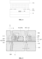
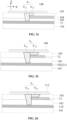
- FIG. 1 shows a display substrate of an advanced super dimension switch type liquid crystal display
- FIG. 2 shows a display substrate of a high aperture-advanced super dimension switch type liquid crystal display
- FIG. 3 shows a display substrate of an in-plane switch type liquid crystal display
- FIG. 4 shows a vertical alignment type liquid crystal display.
- PVX inorganic insulating layer
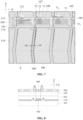
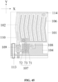
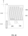
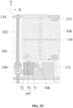
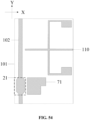
- an embodiment of the present disclosure provides a display substrate, as shown in FIGs. 5 to 22 , the display substrate includes:
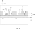
- the display substrate by sequentially arranging a layer of data lines 102, a first insulating layer 103, a layer of gate lines 104, a second insulating layer 105 and a layer of the first electrode 106 on the base substrate 101, two insulating layers, i.e., the first insulating layer 103 and the second insulating layer 105, are simultaneously present between the layer where the data lines 102 are positioned and the layer where the first electrode 106 is positioned that is farther away from the base substrate 101.
- the distance between the layer where the data lines 102 are positioned and the layer where the first electrode 106 is positioned is larger, the coupling capacitance between the data line 102 and the first electrode 106 can be reduced, the load on the data line 102 caused by the coupling capacitance is reduced, the pixel charging rate is favorably improved, and the temperature of a driving chip (IC) is reduced.
- IC driving chip
- the present disclosure reduces the coupling capacitance between the data line 102 and the first electrode 106 utilizing the first insulating layer 103 and the second insulating layer 105 in the related technology, it is not necessary to add an organic insulating layer to reduce the coupling capacitance between the data line 102 and the first electrode 106, and based on this, the process complexity would not be increased.
- the thickness of the first insulating layer 103 is greater than or equal to 3500 ⁇ and less than or equal to 4500 ⁇
- the thickness of the second insulating layer 105 is greater than or equal to 2000 ⁇ and less than or equal to 7000 ⁇ .
- the thickness of the first insulating layer 103 is 4500 ⁇
- the thickness of the second insulating layer 105 is 7000 ⁇ , in which case the thickness of the insulating layer between the data line 102 and the first electrode 106 may be 11500 ⁇ , greatly reducing the load on the data lines 102, and improving the pixel charging rate.
- an orthographic projection of a portion of each of at least a part of the data lines 102 on the base substrate 101 is positioned within the orthographic projection of the first electrode 106 on the base substrate 101.
- the first electrode 106 includes a plurality of slits S, and a minimum distance d1 from the slit S to the data line 102 in the extension direction X of the gate line 104 is greater than 1.5 ⁇ m, in other words, the first electrode 106 may include an electrode strip 106' between two slits S closest to the data line 102, and an orthographic projection of the electrode strip 106' on the base substrate 101 exceeds by at least 1.5 ⁇ m, for example, 2.2 ⁇ m, relative to the orthographic projection of the data line 102 on the base substrate 101. With this arrangement, the electrode strip 106' can cover the data line 102 even after process fluctuation occurs.
- the optimal luminous efficiency design effect of the first electrode 106 can still be achieved.
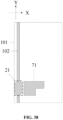
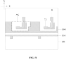
- the display substrate may further include a transistor 107, where a gate 71 of the transistor 107 is disposed in the same layer and made of the same material as the data line 102, a first electrode 72 and a second electrode 73 of the transistor 107 are disposed in the same layer and made of the same material as the gate line 104, so that the transistor 107 is a bottom gate transistor, and light is shielded by the gate 71 of the transistor 107, thereby preventing the light from irradiating the channel of the transistor 107 to affect the stability of the transistor 107.
- the gate 71 of the transistor 107 is electrically connected to a gate line 104, the first electrode 72 of the transistor 107 is electrically connected to a data line 102, and the second electrode 73 of the transistor 107 is electrically connected to a pixel electrode.
- an active layer 74 of the transistor 107 may be made of a material such as amorphous silicon, polysilicon, oxide, or the like; the first electrode 72 of the transistor 107 may be a source and the second electrode 73 of the transistor 107 is a drain, or the first electrode 72 of the transistor 107 is a drain and the second electrode 73 is a source; the transistor 107 may be a P-type transistor or an N-type transistor, which is not limited herein.
- the display substrate may further include a first transfer electrode 108, which is disposed in the same layer and made of the same material as the first electrode 106; the first transfer electrode 108 is electrically connected to the gate 71 of the transistor 107 through a first via V 11 penetrating through the first insulating layer 103 and the second insulating layer 105, and is electrically connected to the gate line 104 through a second via V 12 penetrating through the second insulating layer 105, that is, electrical connection between the gate line 104 and the gate 71 of the transistor 107 is achieved utilizing the first transfer electrode 108.
- the fabrication of the first transfer electrode 108 can be completed at the same time of fabricating the first electrode 106, thereby avoiding an additional process for fabricating the first transfer electrode 108.
- a second via V 12 penetrating through the second insulating layer 105 and used for electrically connecting the first transfer electrode 108 and the gate line 104 and a first via V 11 penetrating through the first insulating layer 103 and the second insulating layer 105 and used for electrically connecting the first transfer electrode 108 and the gate 71 of the transistor 107 can be simultaneously formed in one single patterning process, thereby avoiding an additional process of patterning the first insulating layer 103.
- the gate line 104 may alternatively be electrically connected to the gate 71 of the transistor 107 through a seventh via V 1 ' penetrating through the first insulating layer 103.
- an orthographic projection of the first via V 11 on the base substrate 101 is positioned within the orthographic projection of the gate 71 of the transistor 107 on the base substrate 101, an aperture of the first via V 11 in a direction Z away from the base substrate 101 is gradually increased, and the first via V 11 includes a first port close to the base substrate 101.
- a length B of the first port in an extension direction X of the gate line 104 may be set to be greater than or equal to 3 ⁇ m, and a width F' of the first port in an extension direction Y of the data line 102 is set to be greater than or equal to 6 ⁇ m.
- the length B is 5.75 ⁇ m
- the width F' is 6 ⁇ m.
- an orthographic projection of the second via V 12 on the base substrate 101 is positioned within the orthographic projection of the gate line 104 on the base substrate 101, an aperture of the second via V 12 in a direction Z away from the base substrate 101 is gradually increased, and the second via V 12 includes a second port close to the base substrate 101.
- a length C of the second port in the extension direction X of the gate line 104 may be set to be greater than or equal to 3 ⁇ m, and a width F of the second port in the extension direction Y of the data line 102 is set to be greater than or equal to 8 ⁇ m.
- the length C is 6.25 ⁇ m, and the width F is 8 ⁇ m.
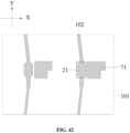
- the gate line 104 includes a protrusion 41 disposed side by side with the first electrode 72 of the transistor 107, the orthographic projection of the first via V 11 on the base substrate 101 is not overlapped with an orthographic projection of the protrusion 41 on the base substrate 101, and the orthographic projection of the second via V 12 on the base substrate 101 is positioned within the orthographic projection of the protrusion 41 on the base substrate 101.
- an area of the protrusion 41 is larger, which facilitates the the lap joint of the protrusion 41 with the first transfer electrode 108 through the second via V 12 .
- a line width of the gate line 104 is increased at only the protrusion 41, so that an overall line width of the gate line 104 is avoided to be larger, and the shielding of the backlight by the gate line 104 is reduced, thus the transmittance is improved.
- the first via V 11 and the second via V 12 may be integrally provided as a first through hole V 1 .
- an orthographic projection of the first through hole V 1 on the base substrate 101 is positioned within the orthographic projection of the first transfer electrode 108 on the base substrate 101, and a one-side excess distance A/D/E/G of the orthographic projection of the first transfer electrode 108 on the base substrate 101 relative to the orthographic projection of the first through hole V 1 on the base substrate 101 in the extension direction Y of the data line 102 and/or the extension direction X of the gate line 104 is greater than or equal to 3 ⁇ m, for example, the one-side excess distances A, D, E, G are 5.55 ⁇ m, 5.75 ⁇ m, 5.5 ⁇ m, respectively.
- the one-side excess distance A/D/E/G of the orthographic projection of the first transfer electrode 108 on the base substrate 101 relative to the orthographic projection of the first through hole V 1 on the base substrate 101 in the extension direction Y of the data line 102 and/or the extension direction X of the gate line 104 is greater than or equal to 3 ⁇ m, even if process fluctuation occurs, the first transfer electrode 108 can still cover the first through hole V 1 well, which reduces the risk of corrosion of the protrusion 41 and the gate 71 caused by moisture contact through the first through hole V 1 .
- an overlapping region OL is formed between the orthographic projection of the protrusion 41 on the base substrate 101 and the orthographic projection of the gate 71 of the transistor 107 on the base substrate 101, and the overlapping region OL is relatively flat to hold a spacer (PS), so that the supporting effect for the spacer (PS) is improved, and the spacer (PS) can be prevented from sliding due to an uneven supporting surface to cause light leakage and the like phenomena.
- the spacer (PS) may alternatively be disposed in other relatively flat regions, and in this case, as shown in FIG. 5 , the orthographic projection of the protrusion 41 on the base substrate 101 and the orthographic projection of the gate 71 of the transistor 107 on the base substrate 101may not be overlapped.
- a minimum distance u between the first electrode 72 of the transistor 107 and the protrusion 41 may be greater than or equal to 5 ⁇ m, for example, 9.55 ⁇ m. Since the first electrode 72 of the transistor 107 and the protrusion 41 are disposed in the same layer and made of the same material, in a case where the minimum distance u between the first electrode 72 of the transistor 107 and the protrusion 41 is greater than or equal to 5 ⁇ m, a short circuit caused by process fluctuation, residual conductive foreign matters (particle), etc. can be avoided.
- the gate line 104 may further include a wiring portion 42 integrally provided with the protrusion 41, and a line width k of the wiring portion 42 in the extension direction Y of the data line 102 is greater than or equal to 5 ⁇ m, for example, 8 ⁇ m, so as to prevent the gate line 104 from breaking.
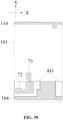
- the wiring portion 42 and the protrusion 41 form an accommodating groove AG, and the first electrode 72 of the transistor 107 is positioned in the accommodating groove AG, so as to prevent the transistor 107 from occupying too much pixel area, and to improve the pixel aperture ratio, and meanwhile to effectively prevent the first electrode 72 of the transistor 107 from being shorted with the gate line 104 disposed in the same layer and made of the same material.
- an opening of the accommodating groove AG faces the pixel electrode controlled, by means of the transistor 107, by the gate line 104 to which the accommodating groove AG belongs, so that the second electrode 73 of the transistor 107 is electrically connected to the pixel electrode at an opening side of the accommodating groove AG.
- the orthographic projection of the gate 71 of the transistor 107 on the base substrate 101 and the orthographic projection of the accommodating groove AG on the base substrate 101 are partially overlapped, so as to facilitate the overlapping of the orthographic projection of the gate 71 of the transistor 107 on the base substrate 101 and the orthographic projection of the first electrode 72 on the base substrate 101 in the accommodating groove AG, thus a channel region in a U-shaped structure of the first electrode 72 forms a conductive channel under the driving of the electric fields of the gate 71 and the first electrode 72.
- the first electrode 72 of the transistor 107 includes a first subsection 721 extending along the extension direction X of the gate line 104, an orthographic projection of the first subsection 721 on the base substrate 101 is partially overlapped with the orthographic projection of the gate 71 of the transistor 107 on the base substrate 101, and is not overlapped with the orthographic projection of the data line 102 on the base substrate 101.
- a distance j between the first subsection 721 and the wiring portion 42 may be set to be greater than or equal to 5 ⁇ m, for example, 9.25 ⁇ m.
- the width i of the first subsection 721 in the extension direction Y of the data line 102 may be set to be greater than or equal to 3 ⁇ m, for example, 6 ⁇ m.
- a minimum distance t between the orthographic projection of the first electrode 72 of the transistor 107 on the base substrate 101 and the orthographic projection of the first transfer electrode 108 on the base substrate 101 is greater than or equal to 3 ⁇ m, for example, 6.55 ⁇ m, so as to prevent the first transfer electrode 108 from being overlapped with the channel region in the U-shaped structure of the first electrode 72 due to factors such as process fluctuations to influence the switching characteristics of the transistor 107.
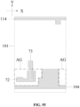
- the display substrate may further include a second transfer electrode 109, which is disposed in the same layer and made of the same material as the first electrode 106; the second transfer electrode 109 is electrically connected to the data line 102 through a third via V 21 penetrating through the first insulating layer 103 and the second insulating layer 105, and is electrically connected to the first electrode 72 of the transistor 107 through a fourth via V 22 penetrating through the second insulating layer 105, i.e., the electrical connection of the data line 102 and the first electrode 72 of the transistor 107 is achieved utilizing the second transfer electrode 109.
- the fabrication of the second transfer electrode 109 can be completed at the same time of fabricating the first electrode 106, thereby avoiding an additional process for fabricating the second transfer electrode 109.
- a via penetrating through the second insulating layer 105 and used for electrically connecting the second transfer electrode 109 and the first electrode 72 of the transistor 107 and a via penetrating through the first insulating layer 103 and the second insulating layer 105 and used for electrically connecting the second transfer electrode 109 and the data line 102 can be simultaneously formed by one patterning process, thereby avoiding an additional process of patterning the first insulating layer 103.
- the first electrode 72 of the transistor 107 may alternatively be electrically connected to the data line 102 through an eighth via V 2 ' penetrating through the first insulating layer 103.
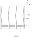
- the data line 102 includes a widened portion 21.
- an orthographic projection of the third via V 21 on the base substrate 101 may be positioned within an orthographic projection of the widened portion 21 on the base substrate 101.
- An aperture of the third via V 21 in a direction Z away from the base substrate 101 is gradually increased.
- the third via V 21 includes a third port close to the base substrate 101, a length b' of the third port in the extension direction X of the gate line 104 is greater than or equal to 6 ⁇ m, and a width e of the third port in the extension direction Y of the data line 102 is greater than or equal to 3 ⁇ m.
- the length b' is 8 ⁇ m
- the width e is 5.75 ⁇ m.
- an area of the widened portion 21 is relatively larger, which facilitates the lap joint of the widened portion 21 with the second transfer electrode 109 through the third via V 21 .
- a line width of the data line 102 is increased at only the widened portion 21, so that an overall line width of the data line 102 is avoided to be larger, and the shielding of the backlight by the data line 102 is reduced, thus the transmittance is improved.
- the first electrode 72 of the transistor 107 includes a second subsection 722, an orthographic projection of the second subsection 722 on the base substrate 101 is positioned within the orthographic projection of the widened portion 21 on the base substrate 101.
- an orthographic projection of the fourth via V 22 on the base substrate 101 is positioned within the orthographic projection of the second subsection 722 on the base substrate 101.
- An aperture of the fourth via V 22 in a direction Z away from the base substrate 101 is gradually increased.
- the fourth via V 22 includes a fourth port close to the base substrate 101, a length b of the fourth port in the extension direction X of the data line 104 is greater than or equal to 8 ⁇ m, and a width f of the fourth port in the extension direction Y of the data line 102 is greater than or equal to 3 ⁇ m.
- the length b is 8 ⁇ m
- the width f is 6.25 ⁇ m.
- the third via V 21 and the fourth via V 22 may be integrally provided as a second through hole V 2 .
- an orthographic projection of the second through hole V 2 on the base substrate 101 is positioned within the orthographic projection of the second transfer electrode 109 on the base substrate 101, and a one-side excess distance a/c/d/g of the orthographic projection of the second transfer electrode 109 on the base substrate 101 relative to the orthographic projection of the second through hole V 2 on the base substrate 101 in the extension direction Y of the data line 102 and/or the extension direction X of the gate line 104 is greater than or equal to 3 ⁇ m.
- the second transfer electrode 109 can still cover the second through hole V 2 well, which reduces the risk of corrosion of the widened portion 21 and the first electrode 72 caused by moisture contact through the second through hole V2.
- a distance h between the widened portion 21 and the gate 71 of the transistor 107 electrically connected to the widened portion 21 may be set to be greater than or equal to 4.8 ⁇ m, for example, 5 ⁇ m.
- the distance between the widened portion 21 and the gate 71 of the transistor 107 adjacent to and unconnected to the widened portion 21 may be increased.
- a distance h between the widened portion 21 and the gate 71 of the transistor 107 adjacent to and unconnected to the widened portion 21 is set to be equal to or greater than 11 ⁇ m, and optionally, the distance h is 13 ⁇ m.
- the orthographic projection of the second transfer electrode 109 on the base substrate 101 is positioned within the orthographic projection of the widened portion 21 on the base substrate 101, so that a sufficient overlap region is present between the data line 102 and the second transfer electrode 109, and a good electrical connection effect between the data line 102 and the second transfer electrode 109 is ensured.
- the orthographic projection of the widened portion 21 on the base substrate 101 may be positioned within the orthographic projection of the accommodating groove AG on the base substrate 101.
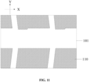
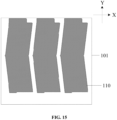
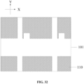
- the display substrate may further include a second electrode 110, which forms a capacitor together with the first electrode 106, the capacitor being a storage capacitor (Cst) or a liquid crystal capacitor (Clc).
- a second electrode 110 which forms a capacitor together with the first electrode 106, the capacitor being a storage capacitor (Cst) or a liquid crystal capacitor (Clc).
- the first electrode 106 of the storage capacitor (Cst) is a pixel electrode
- the first electrode 106 or the second electrode 110 of the liquid crystal capacitor (Clc) is a pixel electrode (P)
- the pixel electrode is electrically connected to the second electrode 73 of the transistor 107.
- the pixel electrode is positioned in a pixel region surrounded by the orthographic projection of the data lines 102 on the base substrate 101 and the orthographic projection of the gate lines 104 on the base substrate 101.
- the orthographic projection of the second electrode 73 of the transistor 107 on the base substrate 101 may be configured to extend from the U-shaped structure of the base substrate 101 till to overlap a part of the of the pixel electrode in the pixel region.
- an orthographic projection of the second electrode 110 on the base substrate 101 is positioned within a region surrounded by orthographic projections of respective data lines 102 on the base substrate 101 and orthographic projections of respective gate lines 104 on the base substrate 101, and a distance d 2 between the orthographic projection of the second electrode 110 on the base substrate 101 and the orthographic projection of the data line 102 on the base substrate 101 is greater than or equal to 6.4 ⁇ m.
- the distance d 2 between the orthographic projection of the second electrode 110 on the base substrate 101 and the orthographic projection of the data line 102 on the base substrate 101 is greater than or equal to 6.4 ⁇ m, not only the second electrode 110 and the data line 102 can be prevented from being overlapped due to process fluctuation, but also the dark region at and near the data line 102 can be prevented from being too large, thereby avoiding a large transmittance loss.
- the second electrode 110 and the data line 102 may be disposed in the same layer and made of different materials.
- the pattern of the second electrode 110 may be first formed using one mask, and then the pattern of the data line 102 may be formed using another mask.
- the second electrode 110 is made of a transparent conductive material such as indium tin oxide (ITO), indium zinc oxide (IZO), or zinc oxide (ZnO).
- a distance d 3 between an orthographic projection of the resistance reduction line 111 on the base substrate 101 and the orthographic projection of the second electrode 110 on the base substrate 101 may be set to be greater than or equal to 4.8 ⁇ m, that is, the orthographic projection of the resistance reduction line 111 on the base substrate 101 exceeds by a distance of 1.6 ⁇ m relative to one side of the orthographic projection of the data line 102 on the base substrate 101.
- the second electrode 110 is made of a transparent conductive material such as indium tin oxide (ITO), indium zinc oxide (IZO), or zinc oxide (ZnO).
- the second electrode 110 is a pixel electrode
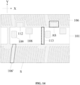
- the display substrate further includes a third transfer electrode 112, which is disposed in the same layer and made of the same material as the first electrode 106.
- the third transfer electrode 112 is electrically connected to the second electrode 106 through a fifth via V 31 penetrating through the first insulating layer 103 and the second insulating layer 105, and is electrically connected to the second electrode 73 of the transistor 107 through a sixth via V 32 penetrating through the second insulating layer 105.
- the fabrication of the third transfer electrode 112 can be completed at the same time of fabricating the first electrode 106, thereby avoiding an additional process for fabricating the third transfer electrode 112.
- a sixth via V 32 penetrating through the second insulating layer 105 and used for electrically connecting the third transfer electrode 108 and the second electrode 73 and a fifth via V 31 penetrating through the first insulating layer 103 and the second insulating layer 105 and used for electrically connecting the third transfer electrode 103 and the second electrode 73 of the transistor 107 can be simultaneously formed by one patterning process, thereby avoiding an additional process of patterning the first insulating layer 103.
- the second electrode 110 may alternatively be electrically connected to the second electrode 73 of the transistor 107 by a ninth via V 3 ' penetrating through the first insulating layer 103.
- an orthographic projection of the fifth via V 31 on the base substrate 101 may be positioned within the orthographic projection of the second electrode 110 on the base substrate 101.
- An aperture of the fifth via V 31 in the direction Z away from the base substrate 101 is gradually increased.
- the fifth via V 31 includes a fifth port close to the base substrate 101, a length m of the fifth port in the extension direction X of the gate line 104 is greater than or equal to 3 ⁇ m, and a width r of the fifth port in the extension direction Y of the data line 102 is greater than or equal to 6 ⁇ m.
- the length m is 4.75 ⁇ m
- the width r is 6 ⁇ m.
- the orthographic projection of the sixth via V 32 on the base substrate 101 may be positioned within an orthographic projection of the second electrode 73 of the transistor 107 on the base substrate 101.
- An aperture of the sixth via V 32 in the direction Z away from the base substrate 101 is gradually increased.
- the sixth via V 32 includes a sixth port close to the base substrate 101, a length n of the sixth port in the extension direction X of the gate line 104 is greater than or equal to 3 ⁇ m, and a width r' of the sixth port in the extension direction Y of the data line 102 is greater than or equal to 8 ⁇ m.
- the length n is 6.25 ⁇ m
- the width r' is 8 ⁇ m.
- the first electrode 106 includes an avoidance slot AS.
- an opening of the avoidance slot AS faces the accommodating groove AG, the third transfer electrode 112 is positioned in the avoidance slot AS, and a distance p between the third transfer electrode 112 and the avoidance slot AS is greater than or equal to 4 ⁇ m, so as to prevent short circuit between the third transfer electrode 112 and the first electrode 106 that are disposed in the same layer and made of the same material.
- the display substrate according to the embodiment of the present disclosure may further include a first connection line 113, which is disposed in the same layer and made of the same material as the first electrode 106, and the first connection line 113 is electrically connected to a non-pixel electrode (such as the first electrode 106 in FIG. 23 ) in the extension direction Y of the data line 102, so that the overall resistance of the non-pixel electrode in the capacitor is relatively small, and meanwhile, the voltage uniformity and stability of the non-pixel electrode in the capacitor in the extension direction Y of the data line 102 are also improved.
- a non-pixel electrode such as the first electrode 106 in FIG. 23
- a distance v between an orthographic projection of the first connection line 113 on the base substrate 101 and the orthographic projection of the protrusion 41 closest to the connection line 113 on the base substrate 101 is greater than or equal to 3 ⁇ m, so as to avoid overlapping of the first connection line 113 and the protrusion 41 caused by process fluctuation and the like.
- a distance x between the orthographic projection of the first connection line 113 on the base substrate 101 and the orthographic projection of a data line 102 (specifically, the widened portion 21 of the data line 102) closest to the connection line 113 on the base substrate 101 is greater than or equal to 4 ⁇ m, so as to avoid overlapping of the first connection line 113 and the data line 102 caused by process fluctuation and the like.
- the width w of the first connection line 113 in the extension direction Y of a gate line 104 is greater than or equal to 4 ⁇ m, so as to prevent the first connection line 113 from breaking.
- the first electrode 106 and the second electrode 110 are overlapped in a region surrounded by the data lines 102 and the gate lines 104 to form a liquid crystal capacitor (Clc), the first electrode 106 is a common electrode (Com) of a slit shape, and the second electrode 110 is a pixel electrode of a block shape.
- a liquid crystal capacitor Lic
- the first electrode 106 is a common electrode (Com) of a slit shape
- the second electrode 110 is a pixel electrode of a block shape.
- the first electrode 106 may be a double domain electrode, and an extension direction of the remaining portion of the data line 102 other than the widened portion 21 may be the same as an extension direction of the double domain electrode, in which case, the extension direction Y of the data line 102 in the present disclosure refers to an overall extension direction of the data line 102, i.e., a column direction.
- the first electrode 106 and the second electrode 110 are overlapped in a region surrounded by the data lines 102 and the gate lines 104 to form a liquid crystal capacitor (Clc), the first electrode 106 is a pixel electrode of a slit shape, the second electrode 110 is a common electrode of a block shape, and the orthographic projection of the first electrode 106 on the base substrate 101 and the orthographic projection of the second electrode 110 on the base substrate 101 are both positioned in only the region surrounded by the data lines 102 and the gate lines 104.
- the second electrode 110 and the data line 102 may be disposed in the same layer with a gap therebetween, and made of different materials. Compared to a scheme where the second electrode 110 and the data line 102 are disposed in different layers, the present disclosure can reduce the number of the film layers, which is favorable for achieving a light and thin product design.
- the first electrode 106 and the second electrode 110 are disposed in the same layer and made of the same material, and both the first electrode 106 and the second electrode 110 have a comb-shaped structure, and the comb-tooth portions of the first electrode 106 and the comb-tooth portions of the second electrode 110 are alternately arranged, so that the first electrode 106 and the second electrode 110 have side surfaces opposite to each other in the same layer to form a liquid crystal capacitor (Clc).
- the first electrode 106 is a pixel electrode electrically connected to the second electrode 73 of the transistor 107, and the second electrode 110 is a common electrode.
- the orthographic projection of the first electrode 106 on the base substrate 101 is only positioned in the region surrounded by the data lines 102 and the gate lines 104, and the orthographic projection of the second electrode 110 on the base substrate 101 is not only positioned in the region surrounded by the data lines 102 and the gate lines 104 but also covers the orthographic projection of most portion of the data line 102 except the widened portion 21 on the base substrate 101, so that the area of the second electrode 110 is larger, and more gaps between the comb-tooth portions can be formed in the second electrode 110 to improve the transmittance and the luminous efficiency.
- the comb-tooth portion of the first electrode 106 and the comb-tooth portion of the second electrode 110 may have a zigzag-shape, for example, a V-shape with an obtuse angle.
- the extension direction of the remaining portion of the data line 102 other than the widened portion 21 may be the same as the extension direction of the comb-tooth portion, in which case, the extension direction Y of the data line 102 in the present disclosure refers to the overall extension direction of the data line 102, i.e., the column direction.
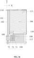
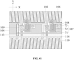
- the common electrodes i.e., the first electrodes 106 in FIGs. 5 to 7 and the second electrodes 110 in FIGs. 30 and 41
- the common electrodes may be further connected by a second connection line 114 to reduce the overall resistance of the common electrodes, and meanwhile, the voltage uniformity and stability of the common electrodes in the extension direction X of the gate line 104 are improved.
- the second connection line 114 may be disposed in the same layer and made of the same material as the gate line 104.
- the second connection line 114 is electrically connected to the common electrode through a via penetrating through the second insulating layer 105.
- the second connection line 114 is electrically connected to the common electrodes of the same row in the extension direction X of the gate line 104 through the a connection line 113 that is disposed in the same layer and made of the same material as the first electrode 106.
- the first electrode 106 and the second electrode 110 constitute a storage capacitor (Cst).
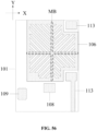
- the first electrode 106 is a slit electrode, and the first electrode 106 includes a cross-shaped main body portion MB, the slits of the first electrode 106 are distributed in four regions defined by the cross-shaped main body portion MB, the extension directions of slits in two regions in the diagonal direction are the same, and the extension directions of slits in two adjacent regions are intersected.
- the second electrode 110 and the data line 102 are disposed in the same layer and made of the same material, and the orthographic projection of the second electrode 110 on the base substrate 101 and an orthographic projection of the cross-shaped main body MB on the base substrate 101 are overlapped.
- second electrodes 110 of the same row in the extension direction X of the gate line 104 may be electrically connected through the first connection line 113, so as to reduce the overall resistance of the second electrodes 110, and meanwhile, the voltage uniformity and stability of the second electrodes 110 in the extension direction X of the gate line 104 are improved.
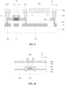
- an embodiment of the present disclosure provides a display panel.
- the display panel includes a display substrate 001 and an opposite substrate 002 that are oppositely arranged, and a liquid crystal layer 003 positioned between the display substrate 001 and the opposite substrate 003, the display substrate 001 being the display substrate 001 according to the embodiment of the present disclosure. Since the problem-solving principle of the display panel is similar to that of the display substrate, the implementation of the display panel according to the embodiment of the present disclosure can refer to the implementation of the display substrate according to the embodiment of the present disclosure, and repeated descriptions are omitted.
- the first electrode 106 includes an electrode strip 106', an orthographic projection of the electrode strip 106' and the orthographic projection of the data line 102 are overlapped.
- the opposite substrate 002 includes a black matrix 201, the black matrix 201 including a first black matrix strip 11 extending along the extension direction Y of the data line 102.
- the orthographic projection of a part of the first black matrix strip 11 on the base substrate 101 is positioned within the orthographic projection of the electrode strip 106' on the base substrate 101. Since the location of the electrode strip 106' is a dark region, disposing the first black matrix strip 11 at the electrode strip 106' would not affect the transmittance.
- the width of the first black matrix strip 11 in the extension direction X of the gate line 104 is greater than or equal to 8 ⁇ m, so that the problem of cross color at oblique viewing angles is avoided through the black matrix strip 11.
- the black matrix 201 may further include a second black matrix strip 12 extending along the extension direction X of the gate line 104.
- the orthographic projection of the gate line 104 on the base substrate 101 is positioned within an orthographic projection of the second black matrix strip 12 on the base substrate 101.
- the display panel according to the embodiment of the present disclosure may further include a sealant surrounding the liquid crystal layer 003 between the display substrate 001 and the opposite substrate 002, a first alignment layer positioned on a side of the display substrate close to the liquid crystal layer, a second alignment layer positioned on a side of the opposite substrate close to the liquid crystal layer, a first polarizer positioned on a side of the display substrate 001 away from the liquid crystal layer 003, a second polarizer positioned on a side of the opposite substrate 002 away from the liquid crystal layer 003, and the like, a polarization direction of the first polarizer being perpendicular to a polarization direction of the second polarizer.
- a sealant surrounding the liquid crystal layer 003 between the display substrate 001 and the opposite substrate 002
- a first alignment layer positioned on a side of the display substrate close to the liquid crystal layer
- a second alignment layer positioned on a side of the opposite substrate close to the liquid crystal layer
- an embodiment of the present disclosure provides a display device including the display panel according to the embodiment of the present disclosure. Since the problem-solving principle of the display device is similar to that of the display panel, the implementation of the display device according to the embodiment of the present disclosure can refer to the implementation of the display panel according to the embodiment of the present disclosure, and repeated descriptions are omitted.
- the display device may further include a backlight module, and the display panel is disposed at a light emitting side of the backlight module.
- the backlight module may be a direct-lit backlight module or an edge-lit backlight module.
- the edge-lit backlight module may include a light bar, and a reflector, a light guide plate, a diffuser, a prism group, and the like that are provided in a stacked manner, the light bar being positioned on a side of the light guide plate in the thickness direction of the light guide.
- the direct-lit backlight module may include a matrix light source, and a reflector, a diffuser plate, a brightness enhancement film, and the like that are provided in a stacked manner at the light-emitting side of the matrix light source, the reflector including an opening disposed directly opposite to the position of each bead in the matrix light source.
- the beads in the light bar and the beads in the matrix light source may be light emitting diodes (LEDs), such as micro light emitting diodes (Mini LED, Micro LED, etc.).
- micro light emitting diodes of sub-millimeter or even micron scale belong to self-light emitting devices.
- the micro light emitting diodes of sub-millimeter or even micron scale have a series of advantages of high brightness, ultralow delay, overlarge visual angle and the like.
- the inorganic light emitting diodes emit light based on a metal semiconductor with more stable property and lower resistance, the inorganic light emitting diodes have the advantages of lower power consumption, higher high temperature resistance and low temperature resistance and longer service life, as compared to organic light emitting diodes that emit light based on organic matters.
- micro light emitting diodes serve as a backlight source
- a more precise dynamic backlight effect can be achieved; the problem of glare between bright and dark regions on a screen caused by traditional dynamic backlight can be solved while effectively improving the screen brightness and the contrast ratio, thereby optimizing the visual experience.
- the display device may be a projector, a 3D printer, a virtual reality device, a mobile phone, a tablet computer, a television, a display, a notebook computer, a digital photo frame, a navigator, an intelligent watch, a fitness wrist strap, a personal digital assistant and any other product or component with a display function.
- the display device includes and is not limited to a radio frequency unit, a network module, an audio output & input unit, a sensor, a display unit, a user input unit, an interface unit, a control chip, or the like.
- the control chip is a central processing unit, a digital signal processor, a system on chip (SoC), or the like.
- control chip may further include a memory, a power module, and the like, and power supply and signal input and output functions are realized through additionally arranged wires, signal lines, and the like.
- control chip may also include a hardware circuit, a computer executable code, and the like.
- the hardware circuit may include a conventional Very Large Scale Integration (VLSI) circuit or gate array, and conventional semiconductors such as logic chips, transistors, or other discrete components; the hardware circuit may also include a field-programmable gate array, programmable array logic, a programmable logic device, or the like.
- VLSI Very Large Scale Integration
- the above-described structure does not constitute a limitation on the above-described display device according to the embodiments of the present disclosure, in other words, the above-described display device according to the embodiments of the present disclosure may include more or less components than the components described above, or some components may be combined, or different component arrangements may be provided.
Landscapes
- Physics & Mathematics (AREA)
- Nonlinear Science (AREA)
- Engineering & Computer Science (AREA)
- Microelectronics & Electronic Packaging (AREA)
- Mathematical Physics (AREA)
- Chemical & Material Sciences (AREA)
- Crystallography & Structural Chemistry (AREA)
- General Physics & Mathematics (AREA)
- Optics & Photonics (AREA)
- Power Engineering (AREA)
- Liquid Crystal (AREA)
- Devices For Indicating Variable Information By Combining Individual Elements (AREA)
Applications Claiming Priority (2)
| Application Number | Priority Date | Filing Date | Title |
|---|---|---|---|
| CN202210817485.8A CN117438430A (zh) | 2022-07-12 | 2022-07-12 | 显示基板及显示装置 |
| PCT/CN2022/141588 WO2024011858A1 (zh) | 2022-07-12 | 2022-12-23 | 显示基板、显示面板及显示装置 |
Publications (2)
| Publication Number | Publication Date |
|---|---|
| EP4443508A1 true EP4443508A1 (de) | 2024-10-09 |
| EP4443508A4 EP4443508A4 (de) | 2025-06-25 |
Family
ID=89535341
Family Applications (1)
| Application Number | Title | Priority Date | Filing Date |
|---|---|---|---|
| EP22950965.8A Pending EP4443508A4 (de) | 2022-07-12 | 2022-12-23 | Anzeigesubstrat, anzeigetafel und anzeigevorrichtung |
Country Status (4)
| Country | Link |
|---|---|
| US (2) | US12235556B2 (de) |
| EP (1) | EP4443508A4 (de) |
| CN (2) | CN117438430A (de) |
| WO (1) | WO2024011858A1 (de) |
Families Citing this family (3)
| Publication number | Priority date | Publication date | Assignee | Title |
|---|---|---|---|---|
| CN119024604A (zh) * | 2023-05-24 | 2024-11-26 | 北京京东方显示技术有限公司 | 显示基板以及显示装置 |
| WO2025161013A1 (zh) * | 2024-02-04 | 2025-08-07 | 京东方科技集团股份有限公司 | 阵列基板、显示面板及显示装置 |
| CN119767786A (zh) * | 2024-12-30 | 2025-04-04 | Tcl华星光电技术有限公司 | 驱动基板及显示面板 |
Family Cites Families (19)
| Publication number | Priority date | Publication date | Assignee | Title |
|---|---|---|---|---|
| JP4813842B2 (ja) * | 2005-07-29 | 2011-11-09 | 株式会社 日立ディスプレイズ | 液晶表示装置 |
| TWI281586B (en) | 2005-09-13 | 2007-05-21 | Ind Tech Res Inst | Pixel array |
| CN100466266C (zh) | 2006-04-21 | 2009-03-04 | 北京京东方光电科技有限公司 | 一种tft lcd阵列基板及制造方法 |
| KR101404551B1 (ko) * | 2008-05-09 | 2014-06-09 | 삼성디스플레이 주식회사 | 박막 트랜지스터 표시판 및 그 제조 방법 |
| WO2010024016A1 (ja) * | 2008-08-28 | 2010-03-04 | シャープ株式会社 | 表示パネル、表示装置及びテレビ受信装置 |
| US9280025B2 (en) * | 2009-03-18 | 2016-03-08 | Unified Innovative Technology, Llc | Active matrix substrate and display device |
| CN103178119B (zh) * | 2013-03-25 | 2015-07-29 | 京东方科技集团股份有限公司 | 阵列基板、阵列基板制备方法以及显示装置 |
| CN103199094B (zh) | 2013-03-25 | 2016-01-20 | 南京中电熊猫液晶显示科技有限公司 | Tft-lcd阵列基板及其制造方法 |
| CN103383946B (zh) * | 2013-07-12 | 2016-05-25 | 京东方科技集团股份有限公司 | 一种阵列基板、显示装置及阵列基板的制备方法 |
| CN104238207A (zh) | 2014-08-22 | 2014-12-24 | 京东方科技集团股份有限公司 | 阵列基板及其制备方法、显示装置 |
| CN105116648A (zh) | 2015-06-26 | 2015-12-02 | 武汉华星光电技术有限公司 | 像素结构、阵列基板及显示装置 |
| CN110189639B (zh) * | 2019-06-28 | 2020-12-04 | 昆山国显光电有限公司 | 显示基板、显示面板及显示装置 |
| US20220128870A1 (en) * | 2019-07-24 | 2022-04-28 | Beijing Boe Display Technology Co., Ltd. | Display substrate and display panel |
| CN210442782U (zh) * | 2019-11-22 | 2020-05-01 | 北京京东方显示技术有限公司 | 一种阵列基板、显示面板、显示装置 |
| CN111146267B (zh) * | 2020-02-19 | 2023-06-02 | 合肥鑫晟光电科技有限公司 | 显示基板及其制造方法、显示装置 |
| CN111403455B (zh) * | 2020-03-27 | 2022-11-11 | 京东方科技集团股份有限公司 | 显示面板及显示装置 |
| CN215895193U (zh) * | 2021-07-27 | 2022-02-22 | 京东方科技集团股份有限公司 | 显示面板和显示装置 |
| CN114594639A (zh) * | 2022-03-09 | 2022-06-07 | 昆山龙腾光电股份有限公司 | 阵列基板及制作方法 |
| CN115016185B (zh) | 2022-06-16 | 2024-01-30 | 武汉华星光电技术有限公司 | 显示面板以及显示面板的制备方法 |
-
2022
- 2022-07-12 CN CN202210817485.8A patent/CN117438430A/zh active Pending
- 2022-12-23 WO PCT/CN2022/141588 patent/WO2024011858A1/zh not_active Ceased
- 2022-12-23 CN CN202280005252.6A patent/CN117693712A/zh active Pending
- 2022-12-23 US US18/580,137 patent/US12235556B2/en active Active
- 2022-12-23 EP EP22950965.8A patent/EP4443508A4/de active Pending
-
2025
- 2025-01-16 US US19/024,340 patent/US20250155762A1/en active Pending
Also Published As
| Publication number | Publication date |
|---|---|
| US12235556B2 (en) | 2025-02-25 |
| CN117693712A (zh) | 2024-03-12 |
| EP4443508A4 (de) | 2025-06-25 |
| WO2024011858A1 (zh) | 2024-01-18 |
| US20240319552A1 (en) | 2024-09-26 |
| CN117438430A (zh) | 2024-01-23 |
| US20250155762A1 (en) | 2025-05-15 |
Similar Documents
| Publication | Publication Date | Title |
|---|---|---|
| EP4443508A1 (de) | Anzeigesubstrat, anzeigetafel und anzeigevorrichtung | |
| US10928686B2 (en) | Array substrate, liquid crystal display panel and display device | |
| US20250271717A1 (en) | Display substrate, display panel and display device | |
| US20240355834A1 (en) | Display substrate, display panel, and display apparatus | |
| EP4564085A1 (de) | Arraysubstrat und anzeigevorrichtung | |
| EP4589376A1 (de) | Arraysubstrat, herstellungsverfahren dafür und anzeigevorrichtung | |
| CN119861512B (zh) | 阵列基板、显示面板及显示装置 | |
| KR20180059020A (ko) | 액정 표시 장치 | |
| CN223966798U (zh) | 显示面板及显示装置 | |
| US12349468B2 (en) | Array substrate and display apparatus | |
| WO2026001341A1 (zh) | 阵列基板、显示面板及显示装置 | |
| EP4589377A1 (de) | Arraysubstrat und anzeigevorrichtung | |
| CN121348618A (zh) | 阵列基板、显示面板及显示装置 | |
| WO2026081148A1 (zh) | 阵列基板、调光面板及显示装置 | |
| WO2025175497A9 (zh) | 显示基板及显示装置 | |
| CN121444008A (zh) | 阵列基板、显示面板及显示装置 | |
| WO2026025490A1 (zh) | 阵列基板、显示面板及显示装置 | |
| WO2026001344A1 (zh) | 一种显示面板及显示装置 | |
| WO2026065240A1 (zh) | 阵列基板、显示面板及显示装置 | |
| WO2025129448A9 (zh) | 阵列基板、显示面板及显示装置 | |
| CN121889721A (zh) | 阵列基板、显示面板及显示装置 | |
| CN120178563A (zh) | 显示面板及显示装置 | |
| CN120178562A (zh) | 阵列基板、显示面板及显示装置 | |
| CN120821122A (zh) | 阵列基板、显示面板及显示装置 | |
| CN117492305A (zh) | 一种显示面板及显示终端 |
Legal Events
| Date | Code | Title | Description |
|---|---|---|---|
| STAA | Information on the status of an ep patent application or granted ep patent |
Free format text: STATUS: THE INTERNATIONAL PUBLICATION HAS BEEN MADE |
|
| PUAI | Public reference made under article 153(3) epc to a published international application that has entered the european phase |
Free format text: ORIGINAL CODE: 0009012 |
|
| STAA | Information on the status of an ep patent application or granted ep patent |
Free format text: STATUS: REQUEST FOR EXAMINATION WAS MADE |
|
| 17P | Request for examination filed |
Effective date: 20240704 |
|
| AK | Designated contracting states |
Kind code of ref document: A1 Designated state(s): AL AT BE BG CH CY CZ DE DK EE ES FI FR GB GR HR HU IE IS IT LI LT LU LV MC ME MK MT NL NO PL PT RO RS SE SI SK SM TR |
|
| REG | Reference to a national code |
Ref country code: DE Ref legal event code: R079 Free format text: PREVIOUS MAIN CLASS: H01L0027120000 Ipc: G02F0001136200 |
|
| A4 | Supplementary search report drawn up and despatched |
Effective date: 20250523 |
|
| RIC1 | Information provided on ipc code assigned before grant |
Ipc: G02F 1/1333 20060101ALN20250519BHEP Ipc: G02F 1/1343 20060101ALN20250519BHEP Ipc: H10D 86/60 20250101ALI20250519BHEP Ipc: H10D 86/00 20250101ALI20250519BHEP Ipc: H10D 86/40 20250101ALI20250519BHEP Ipc: G02F 1/1362 20060101AFI20250519BHEP |
|
| DAV | Request for validation of the european patent (deleted) | ||
| DAX | Request for extension of the european patent (deleted) |