EP4439652B1 - Metallsubstratstruktur und verfahren zur herstellung einer metallsubstratstruktur für ein halbleiterleistungsmodul und halbleiterleistungsmodul - Google Patents
Metallsubstratstruktur und verfahren zur herstellung einer metallsubstratstruktur für ein halbleiterleistungsmodul und halbleiterleistungsmodul Download PDFInfo
- Publication number
- EP4439652B1 EP4439652B1 EP23165917.8A EP23165917A EP4439652B1 EP 4439652 B1 EP4439652 B1 EP 4439652B1 EP 23165917 A EP23165917 A EP 23165917A EP 4439652 B1 EP4439652 B1 EP 4439652B1
- Authority
- EP
- European Patent Office
- Prior art keywords
- metal substrate
- substrate structure
- stress relief
- relief recess
- layer
- Prior art date
- Legal status (The legal status is an assumption and is not a legal conclusion. Google has not performed a legal analysis and makes no representation as to the accuracy of the status listed.)
- Active
Links
Images




Classifications
-
- H—ELECTRICITY
- H10—SEMICONDUCTOR DEVICES; ELECTRIC SOLID-STATE DEVICES NOT OTHERWISE PROVIDED FOR
- H10W—GENERIC PACKAGES, INTERCONNECTIONS, CONNECTORS OR OTHER CONSTRUCTIONAL DETAILS OF DEVICES COVERED BY CLASS H10
- H10W42/00—Arrangements for protection of devices
- H10W42/121—Arrangements for protection of devices protecting against mechanical damage
-
- H—ELECTRICITY
- H10—SEMICONDUCTOR DEVICES; ELECTRIC SOLID-STATE DEVICES NOT OTHERWISE PROVIDED FOR
- H10W—GENERIC PACKAGES, INTERCONNECTIONS, CONNECTORS OR OTHER CONSTRUCTIONAL DETAILS OF DEVICES COVERED BY CLASS H10
- H10W40/00—Arrangements for thermal protection or thermal control
- H10W40/20—Arrangements for cooling
- H10W40/25—Arrangements for cooling characterised by their materials
- H10W40/255—Arrangements for cooling characterised by their materials having a laminate or multilayered structure, e.g. direct bond copper [DBC] ceramic substrates
-
- H—ELECTRICITY
- H10—SEMICONDUCTOR DEVICES; ELECTRIC SOLID-STATE DEVICES NOT OTHERWISE PROVIDED FOR
- H10W—GENERIC PACKAGES, INTERCONNECTIONS, CONNECTORS OR OTHER CONSTRUCTIONAL DETAILS OF DEVICES COVERED BY CLASS H10
- H10W40/00—Arrangements for thermal protection or thermal control
- H10W40/60—Securing means for detachable heating or cooling arrangements, e.g. clamps
- H10W40/611—Bolts or screws
-
- H—ELECTRICITY
- H10—SEMICONDUCTOR DEVICES; ELECTRIC SOLID-STATE DEVICES NOT OTHERWISE PROVIDED FOR
- H10W—GENERIC PACKAGES, INTERCONNECTIONS, CONNECTORS OR OTHER CONSTRUCTIONAL DETAILS OF DEVICES COVERED BY CLASS H10
- H10W40/00—Arrangements for thermal protection or thermal control
- H10W40/60—Securing means for detachable heating or cooling arrangements, e.g. clamps
- H10W40/641—Snap-on arrangements, e.g. clips
-
- H—ELECTRICITY
- H10—SEMICONDUCTOR DEVICES; ELECTRIC SOLID-STATE DEVICES NOT OTHERWISE PROVIDED FOR
- H10W—GENERIC PACKAGES, INTERCONNECTIONS, CONNECTORS OR OTHER CONSTRUCTIONAL DETAILS OF DEVICES COVERED BY CLASS H10
- H10W40/00—Arrangements for thermal protection or thermal control
- H10W40/60—Securing means for detachable heating or cooling arrangements, e.g. clamps
-
- H—ELECTRICITY
- H10—SEMICONDUCTOR DEVICES; ELECTRIC SOLID-STATE DEVICES NOT OTHERWISE PROVIDED FOR
- H10W—GENERIC PACKAGES, INTERCONNECTIONS, CONNECTORS OR OTHER CONSTRUCTIONAL DETAILS OF DEVICES COVERED BY CLASS H10
- H10W90/00—Package configurations
Definitions
- the present disclosure is related to a metal substrate structure and a corresponding method for manufacturing a metal substrate structure for a semiconductor power module.
- the present disclosure is further related to a corresponding semiconductor power module.
- Japanese Patent Application JP 2010 034346 A refers to a metal substrate with circuit metallization layer, metal bottom layer and isolating dielectric layer in-between with fixation areas.
- Japanese Patent Application JP 2006 100640 A refers to a metal substrate with circuit metallization layer, metal bottom layer and isolating dielectric layer in-between with fixation areas.
- US Patent Application US 2019/157182 A1 refers to a metal substrate with metal bottom layer and isolating dielectric layer with fixation areas.
- Embodiments of the disclosure relate to a stable metal substrate structure for a semiconductor power module with a reduced risk of damages occurring. Further embodiments of the disclosure relate to provide a corresponding semiconductor power module and a manufacturing method for such a metal substrate structure.
- a metal substrate structure for a semiconductor power module comprises a circuit metallization layer for conducting electrical signals, e.g. signal and/or current transfer.
- the metal substrate structure further comprises a metal bottom layer that is coupled with the circuit metallization layer, and an isolating dielectric layer that is coupled with and arranged between the circuit metallization layer and the metal bottom layer with respect to a stacking direction of the metal substrate structure.
- the circuit metallization layer or the dielectric layer at least locally forms a top layer of the metal substrate structure, and the top layer and possibly the bottom layer as well comprise a fixation area configured for receiving a fixing element to fix the metal substrate structure to a further component, e.g. a cooler or a heat sink, of the semiconductor power module.
- At least the top layer comprises a stress relief recess that partially or completely surrounds the respective fixation area in a predetermined distance.
- the fixation area can also be referred to a fixation section.
- the metal substrate structure additionally comprises a circuit area.
- the circuit area in particular is the area where the electrical components, like semiconductors chips and their electrical interconnections, are arranged.
- the fixation area and the circuit area are arranged side by side without overlap.
- the fixation area for example is any area outside the circuit area.
- the fixation area is mainly intended for mechanical purposes.
- the one or more stress relief recesses that are associated to a corresponding fixation area can block or stop or at least contribute to hinder a further formation of voids or cracks that my occur during assembling the metal substrate structure by means of fixing elements.
- the described configuration can also contribute to prevent and/or to block delamination of the dielectric layer from the metal bottom layer. A further propagation of damages beyond the stress relief recess is prevented or at least impeded, so that the stress relief recess acts like a firewall.
- the fixation area includes a penetrating fixation opening configured for receiving the fixing element, e.g. a screw or a bolt.
- the stress relief recess is formed such that it partially or completely surrounds the fixation opening in a predetermined distance.
- the stress relief recess is limited by the top layer with a form as a ring- or funnel-shaped groove around the respective fixation area.
- the stress relief recess is limited by the top layer with a conical or V-shape with respect to a cross section through the fixation area and the stress relief recess along the stacking direction.
- the stress relief recess can be limited by the top layer with a rectangular or circular shape with respect to a cross section through the fixation area and the stress relief recess along the stacking direction.
- the stress relief recess penetrates the metallization layer and the dielectric layer.
- the respective stress relief recess can completely or partly penetrate to top layer and hence the metallization layer and/or the dielectric layer.
- the respective stress relief recess can further partly penetrate the metal bottom layer.
- the distance between the stress relief recess and the associated fixation opening or fixation area is given in coordination with the dimensions of the fixing element and with respect to the needed clamping force that is designed to be arranged in the fixation area.
- the stress relief recess is formed in an area to provide electrical isolation of a local portion of the circuit metallization layer being in contact with the fixation element.
- the stress relief recess comprises a predetermined depth along the stacking direction that is equal to or smaller than 2.5 mm.
- the formation of the stress relief recess is configured in coordination with the top layer and/or the bottom layer of the metal substrate structure and/or in coordination with the fixing element that is intended to be used and with respect to the needed clamping force.
- the stress relief recess is formed by at least one of laser cutting, etching and computerized numerical control machining.
- a semiconductor power module comprises a heat sink or cooler unit with a fixation region, e.g. a fixation opening, and an embodiment of the described metal substrate structure.
- the metal substrate structure is fixed to the cooler unit by a fixing element, e.g. a screw, a bolt, a spring and/or a clamp, that is arranged in the fixation area, e.g. in or close to a fixation opening, of the metal substrate structure and in the fixation region of the cooler unit.
- Power semiconductor modules having baseplates, on which substrates with chips are mounted, or insulated metal substrates comprising a relative thick metal plate, an isolating layer, and a circuit metallization, are typically mounted to a cooler by screws or bolts.
- corresponding screw holes, openings or recesses are provided in the baseplate or in the insulated metal substrate.
- a method for manufacturing an embodiment of the metal substrate structure comprises providing a circuit metallization layer for conducting electrical signals, providing a metal bottom layer, and providing an isolating dielectric layer.
- the method further comprises coupling the circuit metallization layer, the metal bottom layer and the dielectric layer with each other such that the dielectric layer is coupled with and arranged between the circuit metallization layer and the metal bottom layer with respect to a stacking direction of the metal substrate structure.
- the circuit metallization layer or the dielectric layer at least locally forms a top layer of the metal substrate structure.
- the method further comprises forming or specifying a fixation area at the top layer and the bottom layer configured for receiving a fixing element to fix the metal substrate structure to a further component of the semiconductor power module.
- the method further comprises forming a stress relief recess at least in the top layer that at least partially surrounds the fixation area in a predetermined distance.
- the step of forming the stress relief recess can comprise forming the stress relief recess by at least one of laser cutting, etching and computerized numerical control machining or any other applicable method.
- the step of providing the dielectric layer can comprise providing a resin sheet or forming the epoxy based resin layer by means of molding, for example.
- a resin sheet is typically filled with particles of dielectric material.
- the described semiconductor power module and the described manufacturing method comprise or are related to produce an embodiment of the metal substrate structure
- described features and characteristics of the metal substrate structure are also disclosed with respect to the semiconductor power module and the manufacturing method and vice versa.
- the fixation element can be realized as a screw or a bolt with an optional washer or spring washer. Alternatively or additionally, the fixation element can comprise a clamp or a spring.
- the stress relief recess is formed as a groove and a location of the groove can be given as surrounding the fixation area of the metal substrate partly or completely.
- the groove can be located next to fixation area or the fixation opening.
- the groove is located next to a semicircular cut-out or recess at an edge of the insulated metal substrate structure.
- a distance between the groove and a screw head or a washer or a spring washer or another fixation structure can have a value within 1-15 mm, for example. Other values are possible as well, in particular dependent on the size of the metal substrate structure. For example, the distance comprises a value between 1-10 mm, 1-5mm or 1-2mm.
- a depth of the groove is predetermined and can penetrate only the circuit metallization layer partly or completely.
- the groove can penetrate the isolating dielectric layer partly or completely.
- the groove may penetrate only the isolation layer partly or completely, assuming there is no circuit metallization layer at that region.
- a bottom portion of the groove can also penetrate into the bottom metal layer.
- the groove may also provide electrical isolation of metal pattern being in contact with a screw or bolt or clamp head, for example.
- a penetration depth can have a value equal to or less than 2.5 mm, assuming the metallization layer has a thickness up to 2.0 mm with respect to the stacking direction.
- the cross-sectional shape of the stress relief recess defined by the limiting contour of the one or more layers of the metal substrate structure can realize a V-cut or can have a round, rectangular or square shape.
- the metal bottom layer of the insulated metal substrate structure can be made of or comprise copper, aluminum, iron, steel, or a corresponding alloy.
- the isolating dielectric layer can be made of or comprise epoxy resin, typically filled with particles of dielectric material, or another isolating material applicable for a lamination or molding process.
- the circuit metallization layer can be made of or comprise copper, aluminum, iron, steel, or a corresponding alloy.
- the insulated metal substrate structure can comprise a relative thick metal base forming the bottom metal layer, an isolating sheet of epoxy resin with inorganic filler, and a circuit metallization layer.
- the metal plate can be completely covered by the isolating sheet and the circuit metallization except from isolating grooves for separation of circuit pattern of different electrical potential.
- screws or bolts can be used as fixing elements for mounting the insulated metal substrate to the cooler unit or another component of the semiconductor power module.
- the screws or bolts are inserted into corresponding holes or attached to recessed portions in peripheral regions, for example.
- a bottom surface of a screw head or of an optional washer gets into contact with the circuit metallization layer or the isolating sheet and exposes pressure and/or torque on the substrate structure, such that also pressure and/or lateral forces at least during the fixation procedure and/or in operation must be considered.
- a pressure and/or torque may result in an uncontrolled delamination or cracking of the layered structure of the insulated metal substrate, which may extend into a circuit area of chips and terminals, where high voltage levels are available. So, the delamination or cracking may significantly reduce the isolation properties and the reliability of the insulated metal substrate.
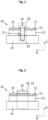
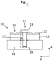
- FIGS. 1 - 6 illustrate different embodiments of a metal substrate structure 10 for a semiconductor power module in respective cross section side views.
- the metal substrate structure 10 comprises a circuit metallization layer 11, a metal bottom layer 13 that coupled with the circuit metallization layer 11, and an isolating dielectric layer 12 that is coupled with and arranged between the circuit metallization layer 11 and the metal bottom layer 13 with respect to a stacking direction A of the metal substrate structure 10.
- the stacking direction A may be orientated perpendicular to a lateral direction B, C of the metal substrate structure 10.
- the circuit metallization layer 11 (see Figs. 1 - 5 or the dielectric layer 12 (see Fig. 6 at least locally forms a top layer of the metal substrate structure 10, and the top layer and the bottom layer 13 comprise a fixation area 18 configured for receiving a fixing element 16 to fix the metal substrate structure 10 to a further component of the semiconductor power module.
- the further component can be realized as a heat sink or a cooler unit 14 as shown in the Figures 1 - 6 .
- the cooler unit 14 comprises a fixation region 19, and the metal substrate structure 10 is fixed to the cooler unit 14 by the fixing element 16 that is arranged in the fixation area 18 of the metal substrate structure 10 and in the fixation region 19 of the cooler unit 14.
- At least the top layer comprises a stress relief recess 15 that partially or completely surrounds the respective fixation area 18 in a predetermined distance.
- the one or more stress relief recesses 15 that are associated to a corresponding fixation area 18, 19 can block or stop or at least contribute to hinder a further formation of voids or cracks that my occur during assembling the metal substrate structure 10 by means of the fixing element 16.
- the progress of damages into a critical region, in particular into a circuit area 20, is blocked by the stress relief recesses 15, such that damages are in particular limited to a certain extension.
- the described configuration can also contribute to prevent delamination of the dielectric layer 12 from the metal bottom layer 13 and/or the metallization layer 11 from the dielectric layer 12.
- the fixation area 18 of the metal substrate structure 10 and the fixation region 19 of the cooler unit 14 include a respective fixation opening 17 and the fixing element 16 is formed as a screw or bolt that extends into the fixation openings 17 and securely fixes the metal substrate structure 10 to the cooler unit 14.
- FIG. 2 shows a different embodiment with a fixing element 16 that is formed as a clamp and the metal substrate structure 10 is fixed to the cooler unit 14 by means of the clamp. Accordingly, there is no need for a fixation opening in the fixation area 18 of the metal substrate structure 10 and the fixation region 19 of the cooler unit 14.
- the stress relief recess 15 can comprise a V-cut cross-sectional shape (see Figs. 1, 2 and 7 ) that can be formed in the metal substrate structure 10 by means of laser processing, for example.
- the stress relief recess 15 can be limited alternatively by the corresponding layers 11, 12 and/or 13 of the metal substrate structure 10 and can comprise a conical shape (see Fig. 3 ), a round or circular shape (see Fig. 4 ) or a rectangular shape (see Fig. 5 .
- FIG. 8 Exemplary top views are illustrated in Fig. 8 and Fig. 9 .
- the stress relief recess 15 can be formed to be limited by one or more of the metallization layer 11, the dielectric layer 12 and the bottom layer 13 of the metal substrate structure 10. According to the Figs. 1-3 the stress relief recess 15 is formed as a V-cut or conical groove that penetrates completely the metallization layer 11 and the dielectric layer 12 and partly the bottom layer 13.
- the stress relief recess 15 is formed as a ring-shaped groove that penetrates completely the metallization layer 11 and partly the dielectric layer 12 and that does not extend into the bottom layer 13.
- the stress relief recess 15 is formed as a rectangular groove as well but the groove penetrates completely the metallization layer 11 and the dielectric layer 12 and extends deeply into the bottom layer 13.
- a depth of the stress relief recess 15 can vary depending on its intended location in the metal substrate structure 10 and/or depending on a respective thickness of the layers 11, 12 and/or 13 of the metal substrate structure 10 and/or depending on the dimensions of the fixing element 16, for example, and depending on the applied force or pressure. This also applies to the other formations of the stress relief recess 15.
- the distance between the stress relief recess 15 and the fixing element 16 is given along the lateral direction B and can be within 1-2 mm, for example.
- the distance can refer to respective center axes of the stress relief recess 15 and the fixing element 16.
- the distance can refer to points of the stress relief recess 15 and the fixing element 16 closest to each other along the lateral direction B or alternatively refer to an average distance. Accordingly, with reference to Fig. 1 the distance can be given with a predetermined value between the inner upper edge of the V-cut stress relief recess 15 and the outer surface of the screw or bolt head.
- the stress relief recess 15 at least surrounds a half of the fixing element 16, the stress relief recess 15 can be formed symmetrically around the fixing element 16 as indicated in the Figs. 1-3 and 5 - 6 . Alternatively, the stress relief recess 15 can be formed asymmetrically with respect to the fixing element 16 as indicated in Fig. 4 .
- the positioning of stress relief recess 15 and the distance between the stress relief recess 15 and the fixing element 16 can vary depending on its intended location in the metal substrate structure 10 and/or depending on a respective thickness of the layers 11, 12 and/or 13 of the metal substrate structure 10 and/or depending on the dimensions of the fixing element 16, for example. This also applies to the other formations of the stress relief recess 15 and the fixing element 16.
- the metal substrate structure 10 comprises the circuit area 20 which for example is arranged in a middle region of the metal substrate structure 10.
- the fixation area 15 is arranged outside of the circuit area 20.
- electric components like semiconductor chips or devices are arranged and electrically connected in the circuit area 20.
- the fixation opening 17 can be surrounded by a plurality of stress relief recesses 15. This is of course possible at the other fixation openings 17, too. It is possible to arrange any feasible number of stress relief recesses 15, for example two, three or four stress relief recesses 15, which are concentrically arranged or arranged in other arrangements to surround the fixation opening.
- Figure 9 shows an embodiment, in which the stress relief recess 15 surrounds the circuit area 20.
- the embodiments of Figures 8 and 9 can be combined, such that the stress relief recesses 15 surround the fixation openings 17 and a further stress relief recess 15 surrounds the circuit area 20. It is also possible that just the stress relief recesses 15 surrounding the fixation openings 17 or just the stress relief recess 15 surrounding the circuit area 20 is arranged. It is possible to arrange any feasible number of stress relief recesses 15 which surround the circuit area 20 (partially or completely), for example two, three or four stress relief recesses 15, which are arranged in layers around the circuit area 20.
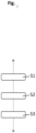
- Figure 7 illustrates a flow chart for a method for manufacturing an embodiment of the metal substrate structure 10.
- the circuit metallization layer 11, the metal bottom layer 13 and the isolating dielectric layer 12 can be provided.
- these layers 11-13 are provided with a given fixation opening 17 for receiving a screw or a bolt.
- a step S2 the circuit metallization layer 11, the metal bottom layer 13 and the dielectric layer 12 are coupled with each other such that the dielectric layer 12 is coupled with and arranged between the circuit metallization layer 11 and the metal bottom layer 13.
- a step S3 one or more stress relief recesses 15 are formed in the circuit metallization layer 11 and/or the dielectric layer 12 and optionally in the metal bottom layer 13 partly as well.
- the step of forming a stress relief recess 15 at least in the top layer can be done by means of laser cutting and/or etching and/or computerized numerical control machining.
- the described embodiments can contribute to reduce a further formation of voids or cracks to at least limited possible damages and/or delamination of the dielectric layer 12 to a certain extension. A further propagation of damages beyond the stress relief recess 15 into the circuit area 20 is prevented or at least impeded, so that the stress relief recess 15 acts like a firewall to protect the circuit area 20.
- the screw head can be in direct contact with the top metallization layer 11, or an optional washer and/or a spring washer can be arranged between the screw head and the top metallization layer 11. So, a mechanical stress on the metal substrate structure 10 cannot be avoided, especially in the vicinity of the fixation elements.
- the described embodiments of the metal substrate structure 10 and its stress relief recess 15 can enable limitation and control of the mechanical stress or a progress of damages to a certain extend.
- the stress relief recess 15 forms a recessed portion or a groove applied on a top surface of the insulated metal substrate structure 10, which at least partly surrounds the screw hole or the location of the screw head or the optional washer in a certain relative distance. If the pressure and/or torque applied by the head of the screw or bolt or clamp causes delamination and/or cracking, the propagation of the delamination or of cracks is stopped or at least hindered at the stress relief recess 15. A further propagation beyond the stress relief recess 15 is prevented or at least impeded, so that the stress relief recess 15 acts like a firewall.
- the described configurations of the metal substrate structure 10 can enable several advantages in view of mounting of corresponding power semiconductor modules to the cooler unit 14.
- the insulated metal substrate structure 10 is a cost-attractive solution especially for low voltage class power modules.
- the proposed metal substrate structure 10 counteracts a negative impact of delamination and/or crack formation, which is caused by the pressure and/or torque exposed by the fixing element 16 due to clamping or screwing. A further propagation of damages beyond the stress relief recess is prevented or at least impeded, so that the stress relief recess acts like a firewall.
- the preparation of a corresponding groove next to the screw positions can be integrated into the preparation process of V-cut grooves, for example, to be used for singulation of substrates.
- the described configurations of the metal substrate structure 10 are applicable for all low voltage products and further products, if a use of an insulated metal substrate is planned.
Landscapes
- Cooling Or The Like Of Semiconductors Or Solid State Devices (AREA)
Claims (18)
- Metallsubstratstruktur (10) für ein Halbleiterleistungsmodul, umfassend:- eine Schaltungsmetallisierungsschicht (11) zum Leiten elektrischer Signale,- eine unterste Metallschicht (13), die mit der Schaltungsmetallisierungsschicht (11) gekoppelt ist, und- eine isolierende dielektrische Schicht (12), die mit der Schaltungsmetallisierungsschicht (11) und der untersten Metallschicht (13) gekoppelt und in Bezug auf eine Stapelrichtung (A) der Metallsubstratstruktur (10) zwischen diesen angeordnet ist, wobei die Schaltungsmetallisierungsschicht (11) oder die dielektrische Schicht (12) zumindest lokal eine oberste Schicht der Metallsubstratstruktur (10) bildet,wobei die oberste Schicht und die unterste Schicht (13) einen Fixierbereich (18) umfassen, der zum Aufnehmen eines Fixierelements (16) zum Fixieren der Metallsubstratstruktur (10) an einer weiteren Komponente (14) des Halbleiterleistungsmoduls ausgelegt ist, und wobei eine Spannungsentlastungsausnehmung (15) die Metallisierungsschicht (11) und die dielektrische Schicht (12) durchdringt.
- Metallsubstratstruktur (10) nach Anspruch 1, wobei die Spannungsentlastungsausnehmung (15) den jeweiligen Fixierbereich (18) zumindest teilweise in einem vorbestimmten Abstand umgibt.
- Metallsubstratstruktur (10) nach Anspruch 2, wobei der Fixierbereich (18) eine durchdringende Fixieröffnung (17) beinhaltet, die zum Aufnehmen des Fixierelements (16) ausgelegt ist, und die Spannungsentlastungsausnehmung (15) die jeweilige Fixieröffnung (17) zumindest teilweise in einem vorbestimmten Abstand umgibt.
- Metallsubstratstruktur (10) nach einem der vorhergehenden Ansprüche, wobei die Spannungsentlastungsausnehmung (15) durch die oberste Schicht mit einer Form wie eine ring- oder trichterförmige Nut um den jeweiligen Fixierbereich (18) herum begrenzt ist.
- Metallsubstratstruktur (10) nach einem der vorhergehenden Ansprüche, wobei die Spannungsentlastungsausnehmung (15) durch die oberste Schicht mit einer konischen oder V-Form in Bezug auf einen Querschnitt durch den Fixierbereich (18) und die Spannungsentlastungsausnehmung (15) entlang der Stapelrichtung (A) begrenzt ist.
- Metallsubstratstruktur (10) nach einem der vorhergehenden Ansprüche, wobei die Spannungsentlastungsausnehmung (15) durch die oberste Schicht mit einer rechteckigen oder kreisförmigen Form in Bezug auf einen Querschnitt durch den Fixierbereich (18) und die Spannungsentlastungsausnehmung (15) entlang der Stapelrichtung (A) begrenzt ist.
- Metallsubstratstruktur (10) nach Anspruch 6, wobei die Spannungsentlastungsausnehmung (15) ferner die unterste Metallschicht (13) teilweise durchdringt.
- Metallsubstratstruktur (10) nach einem der vorhergehenden Ansprüche, wobei der Abstand zwischen der Spannungsentlastungsausnehmung (15) und dem assoziierten Fixierbereich (18) in Koordination mit den Abmessungen des Fixierelements (16) gegeben ist, das dazu ausgelegt ist, in dem Fixierbereich (18) angeordnet zu werden.
- Metallsubstratstruktur (10) nach einem der vorhergehenden Ansprüche, wobei die Spannungsentlastungsausnehmung (15) in einem Bereich ausgebildet ist, um elektrische Isolierung eines lokalen Abschnitts der Schaltungsmetallisierungsschicht (11) bereitzustellen, der mit dem Fixierelement (16) in Kontakt ist.
- Metallsubstratstruktur (10) nach einem der vorhergehenden Ansprüche, wobei die Spannungsentlastungsausnehmung (15) eine vorbestimmte Tiefe entlang der Stapelrichtung (A) umfasst, die gleich oder kleiner als 2,5 mm ist.
- Metallsubstratstruktur (10) nach einem der vorhergehenden Ansprüche, wobei die Spannungsentlastungsausnehmung (15) durch mindestens eines von Laserschneiden, Ätzen und Bearbeitung mittels computergestützter numerischer Steuerung gebildet ist.
- Metallsubstratstruktur (10) nach einem der vorhergehenden Ansprüche, wobei die Spannungsentlastungsausnehmung (15) einen Schaltungsbereich (20) zumindest teilweise in einem vorbestimmten Abstand umgibt.
- Metallsubstratstruktur (10) nach einem der vorhergehenden Ansprüche, wobei die Spannungsentlastungsausnehmung (15) eine Vielzahl von Ausnehmungen (15) umfasst.
- Halbleiterleistungsmodul, umfassend:- eine Kühlereinheit (14) mit einer Fixierregion (19), und- eine Metallsubstratstruktur (10) nach einem der vorhergehenden Ansprüche, wobei die Metallsubstratstruktur (10) durch das Fixierelement (16), das in dem Fixierbereich (18) der Metallsubstratstruktur (10) und in der Fixierregion (19) der Kühlereinheit (14) angeordnet ist, an der Kühlereinheit (14) fixiert ist.
- Halbleiterleistungsmodul nach Anspruch 14, wobei das Fixierelement (16) mindestens eines von einer Schraube, einem Bolzen, einer Klemme und einer Feder umfasst.
- Verfahren zum Herstellen einer Metallsubstratstruktur (10) für ein Halbleiterleistungsmodul, umfassend:- Bereitstellen einer Schaltungsmetallisierungsschicht (11) zum Leiten elektrischer Signale,- Bereitstellen einer untersten Metallschicht (13),- Bereitstellen einer isolierenden dielektrischen Schicht (12),- Koppeln der Schaltungsmetallisierungsschicht (11), der untersten Metallschicht (13) und der dielektrischen Schicht (12) derart miteinander, dass die dielektrische Schicht (12) mit der Schaltungsmetallisierungsschicht (11) und der untersten Metallschicht (13) gekoppelt und in Bezug auf eine Stapelrichtung (A) der Metallsubstratstruktur (10) zwischen diesen angeordnet ist, wobei die Schaltungsmetallisierungsschicht (11) oder die dielektrische Schicht (12) zumindest lokal eine oberste Schicht (10) der Metallsubstratstruktur bildet,- Bilden oder Spezifizieren eines Fixierbereichs (18) an der obersten Schicht und der untersten Schicht (13), der zum Aufnehmen eines Fixierelements (16) ausgelegt ist, um die Metallsubstratstruktur (10) an einer weiteren Komponente des Halbleiterleistungsmoduls (14) zu fixieren, und- Bilden einer Spannungsentlastungsausnehmung (15), die die Metallisierungsschicht (11) und die dielektrische Schicht (12) durchdringt.
- Verfahren nach Anspruch 16, wobei der Schritt des Bildens der Spannungsentlastungsausnehmung (15) zumindest in der obersten Schicht Folgendes umfasst:- Bilden der Spannungsentlastungsausnehmung (15) durch mindestens eines von Laserschneiden, Ätzen und Bearbeitung mittels computergestützter numerischer Steuerung.
- Verfahren nach Anspruch 16 oder 17, wobei der Schritt des Bildens der Spannungsentlastungsausnehmung (15) zumindest in der obersten Schicht Folgendes umfasst:- derartiges Bilden der Spannungsentlastungsausnehmung (15), dass sie den Fixierbereich (18) und/oder einen Schaltungsbereich (20) zumindest teilweise in einem vorbestimmten Abstand umgibt.
Priority Applications (4)
| Application Number | Priority Date | Filing Date | Title |
|---|---|---|---|
| EP23165917.8A EP4439652B1 (de) | 2023-03-31 | 2023-03-31 | Metallsubstratstruktur und verfahren zur herstellung einer metallsubstratstruktur für ein halbleiterleistungsmodul und halbleiterleistungsmodul |
| JP2025555949A JP2026511630A (ja) | 2023-03-31 | 2024-03-14 | 金属基板構造および半導体パワーモジュールのための金属基板構造を製造するための方法ならびに半導体パワーモジュール |
| CN202480023440.0A CN121195346A (zh) | 2023-03-31 | 2024-03-14 | 金属衬底结构及用于制造用于半导体功率模块的金属衬底结构的方法和半导体功率模块 |
| PCT/EP2024/056769 WO2024200019A1 (en) | 2023-03-31 | 2024-03-14 | Metal substrate structure and method for manufacturing a metal substrate structure for a semiconductor power module and semiconductor power module |
Applications Claiming Priority (1)
| Application Number | Priority Date | Filing Date | Title |
|---|---|---|---|
| EP23165917.8A EP4439652B1 (de) | 2023-03-31 | 2023-03-31 | Metallsubstratstruktur und verfahren zur herstellung einer metallsubstratstruktur für ein halbleiterleistungsmodul und halbleiterleistungsmodul |
Publications (2)
| Publication Number | Publication Date |
|---|---|
| EP4439652A1 EP4439652A1 (de) | 2024-10-02 |
| EP4439652B1 true EP4439652B1 (de) | 2025-05-07 |
Family
ID=85795533
Family Applications (1)
| Application Number | Title | Priority Date | Filing Date |
|---|---|---|---|
| EP23165917.8A Active EP4439652B1 (de) | 2023-03-31 | 2023-03-31 | Metallsubstratstruktur und verfahren zur herstellung einer metallsubstratstruktur für ein halbleiterleistungsmodul und halbleiterleistungsmodul |
Country Status (4)
| Country | Link |
|---|---|
| EP (1) | EP4439652B1 (de) |
| JP (1) | JP2026511630A (de) |
| CN (1) | CN121195346A (de) |
| WO (1) | WO2024200019A1 (de) |
Family Cites Families (10)
| Publication number | Priority date | Publication date | Assignee | Title |
|---|---|---|---|---|
| JP4649027B2 (ja) * | 1999-09-28 | 2011-03-09 | 株式会社東芝 | セラミックス回路基板 |
| JP2006100640A (ja) * | 2004-09-30 | 2006-04-13 | Hitachi Metals Ltd | セラミックス回路基板及びこれを用いたパワー半導体モジュール |
| JP4863074B2 (ja) * | 2006-12-05 | 2012-01-25 | 三菱マテリアル株式会社 | 耐割れ性に優れたプラズマエッチング用シリコン電極板 |
| JP5285347B2 (ja) * | 2008-07-30 | 2013-09-11 | セミコンダクター・コンポーネンツ・インダストリーズ・リミテッド・ライアビリティ・カンパニー | 回路装置 |
| JP5225222B2 (ja) * | 2009-07-10 | 2013-07-03 | 京セラ株式会社 | 光半導体素子収納用パッケージ、及び光半導体装置 |
| JP5693395B2 (ja) * | 2011-06-21 | 2015-04-01 | 三菱電機株式会社 | 半導体装置 |
| JP2017050512A (ja) * | 2015-09-04 | 2017-03-09 | 株式会社デンソー | 半導体チップ、半導体装置及び半導体チップの製造方法 |
| JP6827402B2 (ja) * | 2017-11-17 | 2021-02-10 | 三菱電機株式会社 | 半導体装置 |
| JP7077764B2 (ja) * | 2018-05-17 | 2022-05-31 | 株式会社オートネットワーク技術研究所 | 回路装置 |
| JP7298177B2 (ja) * | 2019-02-15 | 2023-06-27 | 富士電機株式会社 | 半導体モジュール及び半導体モジュールの製造方法 |
-
2023
- 2023-03-31 EP EP23165917.8A patent/EP4439652B1/de active Active
-
2024
- 2024-03-14 CN CN202480023440.0A patent/CN121195346A/zh active Pending
- 2024-03-14 WO PCT/EP2024/056769 patent/WO2024200019A1/en not_active Ceased
- 2024-03-14 JP JP2025555949A patent/JP2026511630A/ja active Pending
Also Published As
| Publication number | Publication date |
|---|---|
| EP4439652A1 (de) | 2024-10-02 |
| JP2026511630A (ja) | 2026-04-14 |
| CN121195346A (zh) | 2025-12-23 |
| WO2024200019A1 (en) | 2024-10-03 |
Similar Documents
| Publication | Publication Date | Title |
|---|---|---|
| US9338877B2 (en) | Power electronics assemblies, insulated metal substrate assemblies, and vehicles incorporating the same | |
| EP2779230B1 (de) | Stromüberlagerungsstruktur und Verfahren zur Herstellung davon | |
| TWI389183B (zh) | 堆疊半導體晶片之方法與裝置 | |
| EP0627766B1 (de) | Halbleiteranordnung und Herstellungsverfahren | |
| EP1868244A1 (de) | Halbleiterbauteil | |
| CN110783300B (zh) | 具有调节件及防裂结构的导线架衬底及其覆晶组体 | |
| US11640946B2 (en) | Protection of integrated circuits | |
| EP3823016A1 (de) | Halbleitergehaeuse mit halbleiterchip | |
| EP0661746A1 (de) | Integrierte Schaltungen für Microwellen und deren Herstellung | |
| EP4439652A1 (de) | Metallsubstratstruktur und verfahren zur herstellung einer metallsubstratstruktur für ein halbleiterleistungsmodul und halbleiterleistungsmodul | |
| JP5026025B2 (ja) | 半導体装置 | |
| US20250087623A1 (en) | Packaged semiconductor device having improved reliability and inspectionability and manufacturing method thereof | |
| US10163746B2 (en) | Semiconductor package with improved signal stability and method of manufacturing the same | |
| US6581279B1 (en) | Method of collectively packaging electronic components | |
| EP4080551B1 (de) | Leistungshalbleitermodul und verfahren zur herstellung eines leistungshalbleitermoduls und leistungshalbleiterbauelement | |
| EP4307362A1 (de) | Entwurf für ein hochzuverlässiges halbleitergehäuse | |
| US12183646B2 (en) | Semiconductor device with a dielectric between portions | |
| EP3261416A1 (de) | Halbleiterbauelement | |
| US20210020458A1 (en) | Chip Package and Method of Manufacturing a Chip Package | |
| JP4620994B2 (ja) | 半導体装置 | |
| EP3968372B1 (de) | Verkapseltes halbleiterbauelement mit verbesserter zuverlässigkeit und prüfbarkeit und herstellungsverfahren dafür | |
| EP4057338B1 (de) | Metallsubstratstruktur und verfahren zur herstellung einer metallsubstratstruktur für ein halbleiterleistungsmodul sowie halbleiterleistungsmodul | |
| EP4325557A1 (de) | Halbleitergehäuseanordnung und herstellungsverfahren | |
| US9711424B2 (en) | Low thermal stress package for large area semiconductor dies | |
| EP4432345A1 (de) | Isoliertes metallsubstrat und verfahren zur herstellung eines isolierten metallsubstrats |
Legal Events
| Date | Code | Title | Description |
|---|---|---|---|
| PUAI | Public reference made under article 153(3) epc to a published international application that has entered the european phase |
Free format text: ORIGINAL CODE: 0009012 |
|
| STAA | Information on the status of an ep patent application or granted ep patent |
Free format text: STATUS: REQUEST FOR EXAMINATION WAS MADE |
|
| 17P | Request for examination filed |
Effective date: 20231214 |
|
| AK | Designated contracting states |
Kind code of ref document: A1 Designated state(s): AL AT BE BG CH CY CZ DE DK EE ES FI FR GB GR HR HU IE IS IT LI LT LU LV MC ME MK MT NL NO PL PT RO RS SE SI SK SM TR |
|
| GRAP | Despatch of communication of intention to grant a patent |
Free format text: ORIGINAL CODE: EPIDOSNIGR1 |
|
| STAA | Information on the status of an ep patent application or granted ep patent |
Free format text: STATUS: GRANT OF PATENT IS INTENDED |
|
| INTG | Intention to grant announced |
Effective date: 20241024 |
|
| GRAS | Grant fee paid |
Free format text: ORIGINAL CODE: EPIDOSNIGR3 |
|
| GRAA | (expected) grant |
Free format text: ORIGINAL CODE: 0009210 |
|
| STAA | Information on the status of an ep patent application or granted ep patent |
Free format text: STATUS: THE PATENT HAS BEEN GRANTED |
|
| AK | Designated contracting states |
Kind code of ref document: B1 Designated state(s): AL AT BE BG CH CY CZ DE DK EE ES FI FR GB GR HR HU IE IS IT LI LT LU LV MC ME MK MT NL NO PL PT RO RS SE SI SK SM TR |
|
| REG | Reference to a national code |
Ref country code: GB Ref legal event code: FG4D |
|
| REG | Reference to a national code |
Ref country code: CH Ref legal event code: EP |
|
| REG | Reference to a national code |
Ref country code: DE Ref legal event code: R096 Ref document number: 602023003293 Country of ref document: DE |
|
| REG | Reference to a national code |
Ref country code: IE Ref legal event code: FG4D |
|
| REG | Reference to a national code |
Ref country code: NL Ref legal event code: MP Effective date: 20250507 |
|
| PG25 | Lapsed in a contracting state [announced via postgrant information from national office to epo] |
Ref country code: FI Free format text: LAPSE BECAUSE OF FAILURE TO SUBMIT A TRANSLATION OF THE DESCRIPTION OR TO PAY THE FEE WITHIN THE PRESCRIBED TIME-LIMIT Effective date: 20250507 Ref country code: PT Free format text: LAPSE BECAUSE OF FAILURE TO SUBMIT A TRANSLATION OF THE DESCRIPTION OR TO PAY THE FEE WITHIN THE PRESCRIBED TIME-LIMIT Effective date: 20250908 Ref country code: ES Free format text: LAPSE BECAUSE OF FAILURE TO SUBMIT A TRANSLATION OF THE DESCRIPTION OR TO PAY THE FEE WITHIN THE PRESCRIBED TIME-LIMIT Effective date: 20250507 |
|
| REG | Reference to a national code |
Ref country code: LT Ref legal event code: MG9D |
|
| PG25 | Lapsed in a contracting state [announced via postgrant information from national office to epo] |
Ref country code: NO Free format text: LAPSE BECAUSE OF FAILURE TO SUBMIT A TRANSLATION OF THE DESCRIPTION OR TO PAY THE FEE WITHIN THE PRESCRIBED TIME-LIMIT Effective date: 20250807 Ref country code: GR Free format text: LAPSE BECAUSE OF FAILURE TO SUBMIT A TRANSLATION OF THE DESCRIPTION OR TO PAY THE FEE WITHIN THE PRESCRIBED TIME-LIMIT Effective date: 20250808 |
|
| PG25 | Lapsed in a contracting state [announced via postgrant information from national office to epo] |
Ref country code: NL Free format text: LAPSE BECAUSE OF FAILURE TO SUBMIT A TRANSLATION OF THE DESCRIPTION OR TO PAY THE FEE WITHIN THE PRESCRIBED TIME-LIMIT Effective date: 20250507 Ref country code: PL Free format text: LAPSE BECAUSE OF FAILURE TO SUBMIT A TRANSLATION OF THE DESCRIPTION OR TO PAY THE FEE WITHIN THE PRESCRIBED TIME-LIMIT Effective date: 20250507 |
|
| REG | Reference to a national code |
Ref country code: AT Ref legal event code: MK05 Ref document number: 1793467 Country of ref document: AT Kind code of ref document: T Effective date: 20250507 |
|
| PG25 | Lapsed in a contracting state [announced via postgrant information from national office to epo] |
Ref country code: BG Free format text: LAPSE BECAUSE OF FAILURE TO SUBMIT A TRANSLATION OF THE DESCRIPTION OR TO PAY THE FEE WITHIN THE PRESCRIBED TIME-LIMIT Effective date: 20250507 |
|
| PG25 | Lapsed in a contracting state [announced via postgrant information from national office to epo] |
Ref country code: HR Free format text: LAPSE BECAUSE OF FAILURE TO SUBMIT A TRANSLATION OF THE DESCRIPTION OR TO PAY THE FEE WITHIN THE PRESCRIBED TIME-LIMIT Effective date: 20250507 |
|
| PG25 | Lapsed in a contracting state [announced via postgrant information from national office to epo] |
Ref country code: AT Free format text: LAPSE BECAUSE OF FAILURE TO SUBMIT A TRANSLATION OF THE DESCRIPTION OR TO PAY THE FEE WITHIN THE PRESCRIBED TIME-LIMIT Effective date: 20250507 |
|
| PG25 | Lapsed in a contracting state [announced via postgrant information from national office to epo] |
Ref country code: RS Free format text: LAPSE BECAUSE OF FAILURE TO SUBMIT A TRANSLATION OF THE DESCRIPTION OR TO PAY THE FEE WITHIN THE PRESCRIBED TIME-LIMIT Effective date: 20250807 |
|
| PG25 | Lapsed in a contracting state [announced via postgrant information from national office to epo] |
Ref country code: IS Free format text: LAPSE BECAUSE OF FAILURE TO SUBMIT A TRANSLATION OF THE DESCRIPTION OR TO PAY THE FEE WITHIN THE PRESCRIBED TIME-LIMIT Effective date: 20250907 |
|
| PG25 | Lapsed in a contracting state [announced via postgrant information from national office to epo] |
Ref country code: LV Free format text: LAPSE BECAUSE OF FAILURE TO SUBMIT A TRANSLATION OF THE DESCRIPTION OR TO PAY THE FEE WITHIN THE PRESCRIBED TIME-LIMIT Effective date: 20250507 |
|
| REG | Reference to a national code |
Ref country code: DE Ref legal event code: R079 Ref document number: 602023003293 Country of ref document: DE Free format text: PREVIOUS MAIN CLASS: H01L0023373000 Ipc: H10W0040250000 |
|
| PG25 | Lapsed in a contracting state [announced via postgrant information from national office to epo] |
Ref country code: SM Free format text: LAPSE BECAUSE OF FAILURE TO SUBMIT A TRANSLATION OF THE DESCRIPTION OR TO PAY THE FEE WITHIN THE PRESCRIBED TIME-LIMIT Effective date: 20250507 Ref country code: DK Free format text: LAPSE BECAUSE OF FAILURE TO SUBMIT A TRANSLATION OF THE DESCRIPTION OR TO PAY THE FEE WITHIN THE PRESCRIBED TIME-LIMIT Effective date: 20250507 |
|
| PG25 | Lapsed in a contracting state [announced via postgrant information from national office to epo] |
Ref country code: CZ Free format text: LAPSE BECAUSE OF FAILURE TO SUBMIT A TRANSLATION OF THE DESCRIPTION OR TO PAY THE FEE WITHIN THE PRESCRIBED TIME-LIMIT Effective date: 20250507 |
|
| PG25 | Lapsed in a contracting state [announced via postgrant information from national office to epo] |
Ref country code: EE Free format text: LAPSE BECAUSE OF FAILURE TO SUBMIT A TRANSLATION OF THE DESCRIPTION OR TO PAY THE FEE WITHIN THE PRESCRIBED TIME-LIMIT Effective date: 20250507 |
|
| PG25 | Lapsed in a contracting state [announced via postgrant information from national office to epo] |
Ref country code: SK Free format text: LAPSE BECAUSE OF FAILURE TO SUBMIT A TRANSLATION OF THE DESCRIPTION OR TO PAY THE FEE WITHIN THE PRESCRIBED TIME-LIMIT Effective date: 20250507 |
|
| P01 | Opt-out of the competence of the unified patent court (upc) registered |
Free format text: CASE NUMBER: UPC_APP_0018422_4439652/2025 Effective date: 20251219 |
|
| PG25 | Lapsed in a contracting state [announced via postgrant information from national office to epo] |
Ref country code: IT Free format text: LAPSE BECAUSE OF FAILURE TO SUBMIT A TRANSLATION OF THE DESCRIPTION OR TO PAY THE FEE WITHIN THE PRESCRIBED TIME-LIMIT Effective date: 20250507 |
|
| REG | Reference to a national code |
Ref country code: DE Ref legal event code: R097 Ref document number: 602023003293 Country of ref document: DE |
|
| PLBE | No opposition filed within time limit |
Free format text: ORIGINAL CODE: 0009261 |
|
| STAA | Information on the status of an ep patent application or granted ep patent |
Free format text: STATUS: NO OPPOSITION FILED WITHIN TIME LIMIT |
|
| REG | Reference to a national code |
Ref country code: CH Ref legal event code: L10 Free format text: ST27 STATUS EVENT CODE: U-0-0-L10-L00 (AS PROVIDED BY THE NATIONAL OFFICE) Effective date: 20260318 |
|
| PGFP | Annual fee paid to national office [announced via postgrant information from national office to epo] |
Ref country code: DE Payment date: 20260319 Year of fee payment: 4 |
|
| 26N | No opposition filed |
Effective date: 20260210 |