EP4428900A1 - Procédé de formation d'un contact ohmique sur une couche à base de germanium-étain - Google Patents
Procédé de formation d'un contact ohmique sur une couche à base de germanium-étain Download PDFInfo
- Publication number
- EP4428900A1 EP4428900A1 EP24161328.0A EP24161328A EP4428900A1 EP 4428900 A1 EP4428900 A1 EP 4428900A1 EP 24161328 A EP24161328 A EP 24161328A EP 4428900 A1 EP4428900 A1 EP 4428900A1
- Authority
- EP
- European Patent Office
- Prior art keywords
- germanium
- layer
- nickel
- sputtering
- tin
- Prior art date
- Legal status (The legal status is an assumption and is not a legal conclusion. Google has not performed a legal analysis and makes no representation as to the accuracy of the status listed.)
- Granted
Links
Images

Classifications
-
- H—ELECTRICITY
- H10—SEMICONDUCTOR DEVICES; ELECTRIC SOLID-STATE DEVICES NOT OTHERWISE PROVIDED FOR
- H10D—INORGANIC ELECTRIC SEMICONDUCTOR DEVICES
- H10D64/00—Electrodes of devices having potential barriers
- H10D64/01—Manufacture or treatment
- H10D64/011—Manufacture or treatment of electrodes ohmically coupled to a semiconductor
- H10D64/0111—Manufacture or treatment of electrodes ohmically coupled to a semiconductor to Group IV semiconductors
-
- H—ELECTRICITY
- H10—SEMICONDUCTOR DEVICES; ELECTRIC SOLID-STATE DEVICES NOT OTHERWISE PROVIDED FOR
- H10P—GENERIC PROCESSES OR APPARATUS FOR THE MANUFACTURE OR TREATMENT OF DEVICES COVERED BY CLASS H10
- H10P14/00—Formation of materials, e.g. in the shape of layers or pillars
- H10P14/40—Formation of materials, e.g. in the shape of layers or pillars of conductive or resistive materials
- H10P14/42—Formation of materials, e.g. in the shape of layers or pillars of conductive or resistive materials using a gas or vapour
- H10P14/44—Physical vapour deposition [PVD]
-
- C—CHEMISTRY; METALLURGY
- C23—COATING METALLIC MATERIAL; COATING MATERIAL WITH METALLIC MATERIAL; CHEMICAL SURFACE TREATMENT; DIFFUSION TREATMENT OF METALLIC MATERIAL; COATING BY VACUUM EVAPORATION, BY SPUTTERING, BY ION IMPLANTATION OR BY CHEMICAL VAPOUR DEPOSITION, IN GENERAL; INHIBITING CORROSION OF METALLIC MATERIAL OR INCRUSTATION IN GENERAL
- C23C—COATING METALLIC MATERIAL; COATING MATERIAL WITH METALLIC MATERIAL; SURFACE TREATMENT OF METALLIC MATERIAL BY DIFFUSION INTO THE SURFACE, BY CHEMICAL CONVERSION OR SUBSTITUTION; COATING BY VACUUM EVAPORATION, BY SPUTTERING, BY ION IMPLANTATION OR BY CHEMICAL VAPOUR DEPOSITION, IN GENERAL
- C23C14/00—Coating by vacuum evaporation, by sputtering or by ion implantation of the coating forming material
- C23C14/06—Coating by vacuum evaporation, by sputtering or by ion implantation of the coating forming material characterised by the coating material
- C23C14/14—Metallic material, boron or silicon
- C23C14/16—Metallic material, boron or silicon on metallic substrates or on substrates of boron or silicon
- C23C14/165—Metallic material, boron or silicon on metallic substrates or on substrates of boron or silicon by cathodic sputtering
-
- C—CHEMISTRY; METALLURGY
- C23—COATING METALLIC MATERIAL; COATING MATERIAL WITH METALLIC MATERIAL; CHEMICAL SURFACE TREATMENT; DIFFUSION TREATMENT OF METALLIC MATERIAL; COATING BY VACUUM EVAPORATION, BY SPUTTERING, BY ION IMPLANTATION OR BY CHEMICAL VAPOUR DEPOSITION, IN GENERAL; INHIBITING CORROSION OF METALLIC MATERIAL OR INCRUSTATION IN GENERAL
- C23C—COATING METALLIC MATERIAL; COATING MATERIAL WITH METALLIC MATERIAL; SURFACE TREATMENT OF METALLIC MATERIAL BY DIFFUSION INTO THE SURFACE, BY CHEMICAL CONVERSION OR SUBSTITUTION; COATING BY VACUUM EVAPORATION, BY SPUTTERING, BY ION IMPLANTATION OR BY CHEMICAL VAPOUR DEPOSITION, IN GENERAL
- C23C14/00—Coating by vacuum evaporation, by sputtering or by ion implantation of the coating forming material
- C23C14/22—Coating by vacuum evaporation, by sputtering or by ion implantation of the coating forming material characterised by the process of coating
- C23C14/24—Vacuum evaporation
- C23C14/28—Vacuum evaporation by wave energy or particle radiation
- C23C14/30—Vacuum evaporation by wave energy or particle radiation by electron bombardment
-
- C—CHEMISTRY; METALLURGY
- C23—COATING METALLIC MATERIAL; COATING MATERIAL WITH METALLIC MATERIAL; CHEMICAL SURFACE TREATMENT; DIFFUSION TREATMENT OF METALLIC MATERIAL; COATING BY VACUUM EVAPORATION, BY SPUTTERING, BY ION IMPLANTATION OR BY CHEMICAL VAPOUR DEPOSITION, IN GENERAL; INHIBITING CORROSION OF METALLIC MATERIAL OR INCRUSTATION IN GENERAL
- C23C—COATING METALLIC MATERIAL; COATING MATERIAL WITH METALLIC MATERIAL; SURFACE TREATMENT OF METALLIC MATERIAL BY DIFFUSION INTO THE SURFACE, BY CHEMICAL CONVERSION OR SUBSTITUTION; COATING BY VACUUM EVAPORATION, BY SPUTTERING, BY ION IMPLANTATION OR BY CHEMICAL VAPOUR DEPOSITION, IN GENERAL
- C23C14/00—Coating by vacuum evaporation, by sputtering or by ion implantation of the coating forming material
- C23C14/22—Coating by vacuum evaporation, by sputtering or by ion implantation of the coating forming material characterised by the process of coating
- C23C14/34—Sputtering
- C23C14/3464—Sputtering using more than one target
-
- C—CHEMISTRY; METALLURGY
- C23—COATING METALLIC MATERIAL; COATING MATERIAL WITH METALLIC MATERIAL; CHEMICAL SURFACE TREATMENT; DIFFUSION TREATMENT OF METALLIC MATERIAL; COATING BY VACUUM EVAPORATION, BY SPUTTERING, BY ION IMPLANTATION OR BY CHEMICAL VAPOUR DEPOSITION, IN GENERAL; INHIBITING CORROSION OF METALLIC MATERIAL OR INCRUSTATION IN GENERAL
- C23C—COATING METALLIC MATERIAL; COATING MATERIAL WITH METALLIC MATERIAL; SURFACE TREATMENT OF METALLIC MATERIAL BY DIFFUSION INTO THE SURFACE, BY CHEMICAL CONVERSION OR SUBSTITUTION; COATING BY VACUUM EVAPORATION, BY SPUTTERING, BY ION IMPLANTATION OR BY CHEMICAL VAPOUR DEPOSITION, IN GENERAL
- C23C14/00—Coating by vacuum evaporation, by sputtering or by ion implantation of the coating forming material
- C23C14/22—Coating by vacuum evaporation, by sputtering or by ion implantation of the coating forming material characterised by the process of coating
- C23C14/34—Sputtering
- C23C14/46—Sputtering by ion beam produced by an external ion source
-
- H—ELECTRICITY
- H10—SEMICONDUCTOR DEVICES; ELECTRIC SOLID-STATE DEVICES NOT OTHERWISE PROVIDED FOR
- H10D—INORGANIC ELECTRIC SEMICONDUCTOR DEVICES
- H10D64/00—Electrodes of devices having potential barriers
- H10D64/60—Electrodes characterised by their materials
- H10D64/62—Electrodes ohmically coupled to a semiconductor
Definitions
- the technical field of the invention is that of the formation of an ohmic contact on a layer of a semiconductor material comprising germanium and tin, typically a layer of germanium-tin alloy (GeSn) or silicon-germanium-tin alloy (SiGeSn).
- GeSn and SiGeSn alloys have emerged as promising materials for the realization of microelectronic devices such as field-effect transistors.
- GeSn can be used to form a high-mobility channel in metal-oxide-semiconductor field-effect transistors (MOSFETs) or tunnel field-effect transistors (TFETs). It can also be used in the drain and source regions of a MOSFET to generate compressive stress in a germanium channel.
- MOSFETs metal-oxide-semiconductor field-effect transistors
- TFETs tunnel field-effect transistors
- the GeSn alloy is also used to form the active (emitting/receiving) layers of optoelectronic devices.
- optoelectronic devices include p-i-n photodetectors, heterojunction light-emitting diodes, and more recently, optically and electrically pumped lasers.
- Nickel-based contacts have been proposed because nickel allows the formation of an intermetallic alloy Ni(GeSn) at a temperature compatible with microelectronic and optoelectronic devices, this intermetallic alloy furthermore exhibiting a low specific contact resistivity value ( ⁇ sc) with the GeSn layer and a low square resistance value (Rs).
- Ni(GeSn) contacts exhibit low thermodynamic stability (inducing low thermal stability) due to the segregation of tin atoms and the agglomeration of Ni(GeSn) grains. These segregation and agglomeration phenomena are accentuated when the tin content of the GeSn layer increases.
- the invention aims to form, on a layer of a semiconductor material comprising germanium and tin, an ohmic contact having better thermal stability.
- this objective is achieved by providing a method for forming an ohmic contact comprising a step of depositing a nickel-germanium layer. on the semiconductor material layer using a physical vapor deposition technique.
- the physical vapor deposition technique is selected from evaporation techniques, including thermal evaporation and electron beam evaporation (EBPVD), sputtering techniques, including cathodic sputtering and ion beam sputtering (IBD), ion beam assisted deposition (IBAD) and pulsed laser ablation (PLD).
- evaporation techniques including thermal evaporation and electron beam evaporation (EBPVD), sputtering techniques, including cathodic sputtering and ion beam sputtering (IBD), ion beam assisted deposition (IBAD) and pulsed laser ablation (PLD).
- EBPVD thermal evaporation and electron beam evaporation
- sputtering techniques including cathodic sputtering and ion beam sputtering (IBD), ion beam assisted deposition (IBAD) and pulsed laser ablation (PLD).
- IBD cathodic sputtering and
- the nickel-germanium layer is formed by sputtering a single nickel-germanium target.
- the nickel-germanium layer is formed by co-sputtering a nickel target and a germanium target.
- the forming method may further comprise a step of annealing the nickel-germanium layer at a temperature less than or equal to 350°C, or on the contrary, be devoid of an annealing step.
- FIGS. 2 and 3 schematically represent two modes of implementing a method of forming an ohmic contact on a semiconductor layer 12.
- the semiconductor layer 12 is made of a semiconductor material comprising germanium (Ge) and tin (Sn), such as the germanium-tin alloy (GeSn) or the silicon-germanium-tin alloy (SiGeSn). It can be arranged on a germanium buffer layer 13, itself arranged on a silicon substrate 14.
- the germanium buffer layer 13 and the semiconductor layer 12 have for example been formed (successively) by epitaxy on a silicon substrate 14.
- the semiconductor layer 12 can be epitaxially grown directly on a germanium substrate.
- the semiconductor layer 12 preferably belongs to a semiconductor device which may be a field effect transistor (for example a MOSFET, TFET, etc.), a photodetector (e.g. a pin photodetector), a light-emitting diode (e.g. a heterojunction light-emitting diode) or a laser (e.g. an electrically and optically pumped laser). It may in particular form an active layer of the semiconductor device, such as a channel layer in the case of a FET or a radiation emission or reception layer in the case of optoelectronic devices (photodetector, light-emitting diode and laser).
- the material of the semiconductor layer 12 has an atomic percentage of tin which is advantageously less than or equal to 25% (but not zero), and preferably between 10% and 15% (to obtain a direct gap semiconductor material).
- the method of forming an ohmic contact comprises a step of physical vapor deposition (or PVD) of a nickel-germanium (NiGe) alloy layer 20 on the semiconductor layer 12.
- the electrically conductive NiGe 20 layer forms an ohmic contact with the GeSn-based semiconductor layer 12, without it being necessary to perform annealing to initiate a chemical reaction. It also has the advantage of being thermally stable, unlike a layer composed of the intermetallic alloy Ni(GeSn) and obtained by solid-state reaction of a nickel layer. In particular, when it is subjected to a heat treatment (for example during a subsequent step of the semiconductor device manufacturing process), the NiGe 20 layer does not experience the segregation or agglomeration phenomena of the prior art process. The morphology and crystalline phases of the NiGe 20 layer practically do not change over time. Thus, the NiGe/(Si)GeSn ohmic contact, due to its thermodynamic stability, presents a better resistance to integration than the Ni(GeSn)/(Si)GeSn ohmic contact.
- the NiGe layer 20 is deposited by sputtering a single target 21 made of the NiGe alloy. Such deposition is particularly simple to implement. On the other hand, it is not possible to control the stoichiometry of the NiGe layer 20, since it is fixed by the stoichiometry of the target 21.
- the NiGe target 21 preferably comprises, in atomic percentage (at. %), 40% to 60% of germanium and 60% to 40% of nickel, and even more preferably, 50% of germanium and 50% of nickel.
- the NiGe 20 layer is deposited by co-sputtering (or simultaneous sputtering) of a first target 22a made of nickel and a second target 22b made of germanium.
- This second mode of implementation makes it possible to easily control the composition of the deposited NiGe 20 layer, by adapting the parameters of sputtering of both targets.
- Using two targets is also more cost-effective, as the Ni 22a target and the Ge 22b target are not consumed at the same rate and degrade less quickly over time than a single NiGe target. In addition, it allows for better process control over time.
- the sputtering technique employed in either of these embodiments may be cathodic sputtering (e.g. using an argon plasma, as shown in the Figures 2-3 ) or ion beam deposition (IBD).
- cathodic sputtering e.g. using an argon plasma, as shown in the Figures 2-3
- IBD ion beam deposition
- An XRD (X-Ray Diffraction) analysis of the sputter-deposited NiGe 20 layer revealed the presence of four crystalline phases ((111), (112), (211) and (013)), i.e. a polycrystalline state.
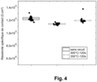
- NiGe/GeSn ohmic contacts obtained using the forming method according to the invention have a specific contact resistivity comparable to that of the Ni(GeSn)/GeSn contacts and that, in addition, this specific contact resistivity is only very slightly improved by annealing the NiGe layer at a temperature less than or equal to 350°C.
- the forming method according to the invention may be devoid of an annealing step after the PVD step. It is then faster (and less expensive) to implement.
- the forming method according to the invention only comprises the PVD step (single-step process).
- the NiGe 20 layer can be annealed at a temperature lower than or equal to 350 °C, in order to improve the specific contact resistivity by a few percent.
- PVD techniques other than sputtering techniques may be employed to form an ohmic NiGe contact on the semiconductor layer 12.
- examples include evaporation techniques, including thermal evaporation and electron beam PVD (EBPVD).
- the evaporation equipment may include a single crucible containing a source of NiGe (e.g., in the form of pellets or billets) or two crucibles, one containing a source of nickel and the other containing a source of germanium.
- the NiGe 20 layer can also be obtained by ion beam-assisted deposition (IBAD) or pulsed laser ablation (PLD), using a single NiGe target.
- IBAD ion beam-assisted deposition
- PLD pulsed laser ablation
Landscapes
- Chemical & Material Sciences (AREA)
- Chemical Kinetics & Catalysis (AREA)
- Engineering & Computer Science (AREA)
- Materials Engineering (AREA)
- Mechanical Engineering (AREA)
- Metallurgy (AREA)
- Organic Chemistry (AREA)
- Health & Medical Sciences (AREA)
- Toxicology (AREA)
- Electrodes Of Semiconductors (AREA)
Abstract
Description
- Le domaine technique de l'invention est celui de la formation d'un contact ohmique sur une couche en un matériau semi-conducteur comprenant du germanium et de l'étain, typiquement une couche en alliage germanium-étain (GeSn) ou en alliage silicium-germanium-étain (SiGeSn).
- Les alliages GeSn et SiGeSn sont apparus comme des matériaux prometteurs pour la réalisation de dispositifs microélectroniques comme les transistors à effet de champ. Par exemple, le GeSn peut être utilisé pour former un canal de haute mobilité dans les transistors à effet de champ à structure métal-oxyde-semiconducteur (ou MOSFET, pour « metal-oyde-semiconductor field effect transistor » en anglais) ou dans les transistors à effet de champ à effet tunnel (ou TFET, pour « tunnel field effect transistor » en anglais). Il peut également être utilisé dans les régions de drain et de source d'un MOSFET pour générer une contrainte en compression dans un canal en germanium.
- Puisque l'ajout d'étain dans la structure cristalline du germanium au-delà d'un pourcentage atomique d'environ 10 % permet d'obtenir un matériau semi-conducteur à bande interdite directe, l'alliage GeSn est également utilisé pour former les couches actives (émettrices/réceptrices) de dispositifs optoélectroniques. On peut citer à titre d'exemple de dispositifs optoélectroniques les photodétecteurs p-i-n, les diodes électroluminescentes à hétérojonction et, plus récemment, les lasers à pompage optique et électrique.
- Quelle que soit l'application visée, des contacts ohmiques peu résistifs avec la couche de GeSn sont nécessaires pour obtenir des dispositifs performants.
- Des contacts à base de nickel ont été proposés, car le nickel permet la formation d'un alliage intermétallique Ni(GeSn) à une température compatible avec les dispositifs microélectroniques et optoélectroniques, cet alliage intermétallique présentant en outre une faible valeur de résistivité spécifique de contact (ρsc) avec la couche de GeSn et une faible valeur de résistance carrée (Rs).
- Les articles [« Formation of Ni(Ge1-xSnx) layers with solid-phase reaction in Ni/Ge1-xSnx/Ge systems », Tsuyoshi Nishimura et al., Solid-State Electronics, Volume 60, Issue 1, pp. 46-52, 2011] et [« Impact of alloying éléments (Co, Pt) on nickel stanogermanide formation », Andrea Quintero et al., Materials Science in Semiconductor Processing, 108, 104890, 2020] décrivent ainsi des procédés de formation de contact ohmique par réaction à l'état solide d'une couche de nickel sur une couche de GeSn.
- La
figure 1 représente schématiquement le procédé de formation de contact ohmique décrit dans l'article de A. Quintero et al. Le procédé de formation comprend deux étapes : - une étape S1 de dépôt par pulvérisation d'une couche de nickel 11 sur une couche de GeSn 12, la couche de GeSn 12 ayant été préalablement formée par épitaxie sur une couche tampon en germanium 13, elle-même épitaxiée sur un substrat en silicium 14 ; et
- une étape S2 de recuit de l'empilement ainsi obtenu à une température comprise entre 200 °C et 550 °C pendant 30 s, pour former une couche de Ni(GeSn) 15 en contact ohmique avec la couche de GeSn 12.
- Comme indiqué dans les articles précités, les contacts Ni(GeSn) présentent une faible stabilité thermodynamique (induisant une faible stabilité thermique) liée à la ségrégation des atomes d'étain et à l'agglomération des grains de Ni(GeSn). Ces phénomènes de ségrégation et d'agglomération sont accentués lorsque la teneur en étain de la couche de GeSn augmente.
- L'invention vise à former, sur une couche en un matériau semi-conducteur comprenant du germanium et de l'étain, un contact ohmique présentant une meilleure stabilité thermique.
- Selon l'invention, on tend vers cet objectif en prévoyant un procédé de formation de contact ohmique comprenant une étape de dépôt d'une couche de nickel-germanium sur la couche de matériau semi-conducteur au moyen d'une technique de dépôt physique en phase vapeur.
- De préférence, la technique de dépôt physique en phase vapeur est choisie parmi les techniques d'évaporation, notamment l'évaporation thermique et l'évaporation par faisceau d'électrons (EBPVD), les techniques de pulvérisation, notamment la pulvérisation cathodique et la pulvérisation par faisceau d'ions (IBD), le dépôt assisté par faisceau d'ion (IBAD) et l'ablation laser pulsé (PLD).
- Dans un premier mode de mise en oeuvre du procédé de formation, la couche de nickel-germanium est formée par pulvérisation d'une unique cible de nickel-germanium.
- Dans un deuxième mode de mise en oeuvre, la couche de nickel-germanium est formée par co-pulvérisation d'une cible de nickel et d'une cible de germanium.
- Le procédé de formation peut comprendre en outre une étape de recuit de la couche de nickel-germanium à une température inférieure ou égale à 350 °C, ou au contraire, être dépourvu d'étape de recuit.
- Le procédé de formation selon l'invention peut également présenter une ou plusieurs des caractéristiques ci-dessous, considérées individuellement ou selon toutes les combinaisons techniquement possibles :
- le matériau semi-conducteur est du germanium-étain ou du silicium-germanium-étain ;
- le matériau semi-conducteur présente un pourcentage atomique d'étain inférieur ou égal à 25 % ;
- la couche de matériau semi-conducteur appartient à un dispositif semiconducteur de type transistor à effet de champ, photodétecteur, diode électroluminescente ou laser.
- D'autres caractéristiques et avantages de l'invention ressortiront clairement de la description qui en est donnée ci-dessous, à titre indicatif et nullement limitatif, en référence aux figures suivantes :
- la
figure 1 représente schématiquement un procédé de formation de contact ohmique selon l'art antérieur ; - la
figure 2 représente schématiquement un premier mode de mise en oeuvre du procédé de formation de contact ohmique selon l'invention ; - la
figure 3 représente schématiquement un deuxième mode de mise en oeuvre du procédé de formation de contact ohmique selon l'invention ; et - la
figure 4 représente la résistivité spécifique de contact d'une pluralité de contacts ohmiques obtenus grâce au procédé de formation selon l'invention, avec ou sans une étape de recuit après l'étape de dépôt. - Pour plus de clarté, les éléments identiques ou similaires sont repérés par des signes de référence identiques sur l'ensemble des figures.
- Les
figures 2 et 3 représentent schématiquement deux modes de mise en oeuvre d'un procédé de formation d'un contact ohmique sur une couche semi-conductrice 12. - La couche semi-conductrice 12 est constituée d'un matériau semi-conducteur comprenant du germanium (Ge) et de l'étain (Sn), tel que l'alliage germanium-étain (GeSn) ou l'alliage silicium-germanium-étain (SiGeSn). Elle peut être disposée sur une couche tampon en germanium 13, elle-même disposée sur un substrat en silicium 14. La couche tampon en germanium 13 et la couche semi-conductrice 12 ont par exemple été formées (successivement) par épitaxie sur un substrat 14 en silicium. Alternativement, la couche semi-conductrice 12 peut être épitaxiée directement sur un substrat en germanium.
- La couche semi-conductrice 12 appartient de préférence à un dispositif semi-conducteur qui peut être un transistor à effet de champ (par exemple un MOSFET, TFET...), un photodétecteur (ex. un photodétecteur p-i-n), une diode électroluminescente (ex. une diode électroluminescente à hétérojonction) ou un laser (ex. un laser à pompage électrique et optique). Elle peut notamment former une couche active du dispositif semi-conducteur, telle qu'une couche de canal dans le cas d'un FET ou une couche d'émission ou de réception de rayonnement dans le cas des dispositifs optoélectroniques (photodétecteur, diode électroluminescente et laser). Le matériau de la couche semi-conductrice 12 présente un pourcentage atomique d'étain qui est avantageusement inférieur ou égal à 25 % (mais non nul), et de préférence compris entre 10 % et 15 % (pour obtenir un matériau semi-conducteur à gap direct).
- D'une manière commune aux deux modes de réalisation, le procédé de formation de contact ohmique comprend une étape de dépôt physique en phase vapeur (ou PVD, pour « physical vapor déposition » en anglais) d'une couche en alliage de nickel-germanium (NiGe) 20 sur la couche semi-conductrice 12.
- La couche de NiGe 20, électriquement conductrice, forme un contact ohmique avec la couche semi-conductrice 12 à base de GeSn, sans qu'il ne soit nécessaire d'accomplir un recuit pour initier une réaction chimique. Elle présente en outre l'avantage d'être stable thermiquement, contrairement à une couche composée de l'alliage intermétallique Ni(GeSn) et obtenue par réaction à l'état solide d'une couche de nickel. En particulier, lorsqu'elle est soumise à un traitement thermique (par exemple lors d'une étape ultérieure du procédé de fabrication du dispositif semi-conducteur), la couche de NiGe 20 ne connait pas les phénomènes de ségrégation ou d'agglomération du procédé de l'art antérieur. La morphologie et les phases cristallines de la couche de NiGe 20 n'évoluent pratiquement pas dans le temps. Ainsi, le contact ohmique NiGe/(Si)GeSn, de par sa stabilité thermodynamique, présente une meilleure résistance à l'intégration que le contact ohmique Ni(GeSn)/(Si)GeSn.
- Dans le premier mode de mise en oeuvre représenté par la
figure 2 , la couche de NiGe 20 est déposée par pulvérisation d'une unique cible 21 constituée de l'alliage NiGe. Un tel dépôt est particulièrement simple à mettre en oeuvre. En revanche, il n'est pas possible de contrôler la stoechiométrie de la couche de NiGe 20, car celle-ci est fixée par la stoechiométrie de la cible 21. La cible de NiGe 21 comprend de préférence, en pourcentage atomique (at. %), 40 % à 60 % de germanium et 60 % à 40 % de nickel, et plus préférentiellement encore, 50 % de germanium et 50 % de nickel. - Dans le deuxième mode de mise en oeuvre représenté par la
figure 3 , la couche de NiGe 20 est déposée par co-pulvérisation (ou pulvérisation simultanée) d'une première cible 22a constituée de nickel et d'une deuxième cible 22b constituée de germanium. Ce deuxième mode de mise en oeuvre permet de contrôler facilement la composition de la couche de NiGe 20 déposée, en adaptant les paramètres de pulvérisation des deux cibles. Utiliser deux cibles est également plus avantageux en termes de coût, car la cible de Ni 22a et la cible de Ge 22b ne sont pas consommées à la même vitesse et se dégradent moins vite dans le temps qu'une unique cible de NiGe. En outre, cela permet une meilleure maitrise du procédé au fil du temps. - La technique de pulvérisation employée dans l'un ou l'autre de ces modes de mise en oeuvre peut être la pulvérisation cathodique (en utilisant par exemple un plasma d'argon, comme représentée sur les
figures 2-3 ) ou la pulvérisation par faisceau d'ions (ou IBD, pour « ion beam déposition » en anglais). - A titre d'exemple, la couche de NiGe 20 peut être déposée à une vitesse d'environ 0,25 nm/s par pulvérisation cathodique d'une unique cible de NiGe (
Fig.2 ) au moyen du réacteur de pulvérisation Alliance Concept CT200, dans les conditions suivantes : - un débit d'argon de 50 sccm (abréviation de « Standard Cubic Centimeter per Minute » en anglais, soit le nombre de cm3 de gaz s'écoulant par minute dans les conditions standard de pression et de température, i.e. à une température de 0 °C et une pression de 1013,25 hPa) ;
- une pression dans la chambre du réacteur égale à 2 mTorr, soit 0,267 Pa ;
- une puissance émise par le générateur DC du réacteur égale à 1000 W ;
- une vitesse de rotation du porte-substrat égale à 15 trs/min ; et
- une température de porte-substrat égale à 70 °C.
- Une analyse par XRD (« X-Ray Diffraction » en anglais) de la couche de NiGe 20 déposée par pulvérisation a révélé la présence de quatre phases cristallines ((111), (112), (211) et (013)), autrement dit un état polycristallin.
- La
figure 4 représente des mesures de la résistivité spécifique de contact pour trois séries d'échantillons de contact NiGe/GeSn : - une première série d'échantillons pour laquelle le dépôt de la couche de NiGe 20 n'est pas suivi d'étape de recuit ;
- une deuxième série d'échantillons pour laquelle le dépôt de la couche de NiGe 20 est suivi d'une étape de recuit à 300 °C pendant 120 s ; et
- une troisième série d'échantillons pour laquelle le dépôt de la couche de NiGe 20 est suivi d'une étape de recuit à 350 °C pendant 120 s.
- Ces mesures montrent que les contacts ohmiques NiGe/GeSn obtenus grâce au procédé de formation selon l'invention présentent une résistivité spécifique de contact comparable à celle des contacts Ni(GeSn)/GeSn et qu'en outre, cette résistivité spécifique de contact n'est que très légèrement améliorée par le recuit de la couche de NiGe à une température inférieure ou égale à 350 °C.
- Ainsi, contrairement au procédé de formation par réaction à l'état solide de l'art antérieur, le procédé de formation selon l'invention peut être dépourvu d'étape de recuit après l'étape de PVD. Il est alors plus rapide (et moins coûteux) à mettre en oeuvre. Avantageusement, le procédé de formation selon l'invention ne comprend que l'étape de PVD (procédé en une seule étape).
- Alternativement, la couche de NiGe 20 peut être soumise à un recuit à une température inférieure ou égale à 350 °C, afin d'améliorer de quelques pourcents la résistivité spécifique de contact.
- Des techniques de PVD autres que les techniques de pulvérisation peuvent être employées pour former un contact ohmique NiGe sur la couche semi-conductrice 12. On peut citer à titre d'exemple les techniques d'évaporation, notamment l'évaporation thermique et l'évaporation par faisceau d'électrons (ou EBPVD, pour « electron beam PVD »). L'équipement d'évaporation peut comprendre un seul creuset contenant une source de NiGe (par exemple sous la forme de granulés ou billettes) ou deux creusets, l'un contenant une source de nickel et l'autre contenant une source de germanium.
- La couche de NiGe 20 peut aussi être obtenue par un dépôt assisté par faisceau d'ions (ou IBAD, pour « ion beam-assisted déposition ») ou par ablation laser pulsé (ou PLD, pour « pulsed laser déposition »), en utilisant une unique cible de NiGe.
Claims (9)
- Procédé de formation d'un contact ohmique sur une couche (12) en un matériau semi-conducteur comprenant du germanium et de l'étain, comprenant une étape de dépôt d'une couche de nickel-germanium (20) sur la couche de matériau semi-conducteur (12) au moyen d'une technique de dépôt physique en phase vapeur.
- Procédé selon la revendication 1, dans lequel la technique de dépôt physique en phase vapeur est choisie parmi les techniques d'évaporation, notamment l'évaporation thermique et l'évaporation par faisceau d'électrons (EBPVD), les techniques de pulvérisation, notamment la pulvérisation cathodique et la pulvérisation par faisceau d'ions (IBD), le dépôt assisté par faisceau d'ion (IBAD) et l'ablation laser pulsé (PLD).
- Procédé selon l'une des revendications 1 et 2, dans lequel la couche de nickel-germanium (20) est formée par pulvérisation d'une unique cible de nickel-germanium (21).
- Procédé selon l'une des revendications 1 et 2, dans lequel la couche de nickel-germanium (20) est formée par co-pulvérisation d'une cible de nickel (22a) et d'une cible de germanium (22b).
- Procédé selon l'une quelconque des revendications 1 à 4, comprenant en outre une étape de recuit de la couche de nickel-germanium (20) à une température inférieure ou égale à 350 °C.
- Procédé selon l'une quelconque des revendications 1 à 4, dépourvu d'étape de recuit.
- Procédé selon l'une quelconque des revendications 1 à 6, dans lequel le matériau semi-conducteur est du germanium-étain (GeSn) ou du silicium-germanium-étain (SiGeSn).
- Procédé selon l'une quelconque des revendications 1 à 7, dans lequel le matériau semi-conducteur présente un pourcentage atomique d'étain inférieur ou égal à 25 %.
- Procédé selon l'une quelconque des revendications 1 à 8, dans lequel la couche de matériau semi-conducteur appartient à un dispositif semiconducteur de type transistor à effet de champ, photodétecteur, diode électroluminescente ou laser.
Applications Claiming Priority (1)
| Application Number | Priority Date | Filing Date | Title |
|---|---|---|---|
| FR2302062A FR3146543B1 (fr) | 2023-03-06 | 2023-03-06 | Procédé de formation d’un contact ohmique sur une couche à base de germanium-étain |
Publications (2)
| Publication Number | Publication Date |
|---|---|
| EP4428900A1 true EP4428900A1 (fr) | 2024-09-11 |
| EP4428900B1 EP4428900B1 (fr) | 2025-09-24 |
Family
ID=87136090
Family Applications (1)
| Application Number | Title | Priority Date | Filing Date |
|---|---|---|---|
| EP24161328.0A Active EP4428900B1 (fr) | 2023-03-06 | 2024-03-05 | Procédé de formation d'un contact ohmique sur une couche à base de germanium-étain |
Country Status (3)
| Country | Link |
|---|---|
| US (1) | US20240304451A1 (fr) |
| EP (1) | EP4428900B1 (fr) |
| FR (1) | FR3146543B1 (fr) |
-
2023
- 2023-03-06 FR FR2302062A patent/FR3146543B1/fr active Active
-
2024
- 2024-03-05 EP EP24161328.0A patent/EP4428900B1/fr active Active
- 2024-03-06 US US18/597,346 patent/US20240304451A1/en active Pending
Non-Patent Citations (3)
| Title |
|---|
| ANDREA QUINTERO ET AL.: "Impact of alloying éléments (Co, Pt) on nickel stanogermanide formation", MATERIALS SCIENCE IN SEMICONDUCTOR PROCESSING, vol. 108, 2020, pages 104890 |
| QUINTERO A ET AL: "Impact of Sn content in Ge1-xSnx layers on Ni-stanogermanides solid-state reaction and properties", 2018 IEEE INTERNATIONAL INTERCONNECT TECHNOLOGY CONFERENCE (IITC), IEEE, 4 June 2018 (2018-06-04), pages 103 - 105, XP033386028, DOI: 10.1109/IITC.2018.8430475 * |
| TSUYOSHI NISHIMURA ET AL.: "Formation of Ni(Ge Sn ) layers with solid-phase reaction in Ni/Ge Sn /Ge systems", SOLID-STATE ELECTRONICS, vol. 60, 2011, pages 46 - 52, XP028199289, DOI: 10.1016/j.sse.2011.01.025 |
Also Published As
| Publication number | Publication date |
|---|---|
| US20240304451A1 (en) | 2024-09-12 |
| FR3146543B1 (fr) | 2025-02-28 |
| FR3146543A1 (fr) | 2024-09-13 |
| EP4428900B1 (fr) | 2025-09-24 |
Similar Documents
| Publication | Publication Date | Title |
|---|---|---|
| US11488920B2 (en) | Silver nano-twinned thin film structure and method for forming the same | |
| EP0000317A1 (fr) | Procédé de fabrication d'une électrode en siliciure sur un substrat notamment semi-conducteur | |
| EP2989656B1 (fr) | Procédé de fabrication d'une diode schottky sur un substrat en diamant | |
| FR2738394A1 (fr) | Dispositif a semi-conducteur en carbure de silicium, et son procede de fabrication | |
| FR2475295A1 (fr) | Diode et dispositif rom ou eeprom utilisant cette diode | |
| FR2464565A1 (fr) | Pile solaire au silicium amorphe | |
| FR3002081A1 (fr) | Plaquette composite et son procede de fabrication | |
| FR2929755A1 (fr) | Procede de traitement d'un substrat semi-conducteur par activation thermique d'elements legers | |
| EP1861882A1 (fr) | Procede de fabrication d'une cellule photovoltaique a base de silicium en couche mince | |
| TWI803984B (zh) | 金屬薄膜表面奈米孿晶結構及其形成方法 | |
| CN109994563A (zh) | 用于制造薄层太阳能模块的方法以及按照该方法可获得的薄层太阳能模块 | |
| FR2548219A1 (fr) | Procede de formation d'une couche de matiere a constituants multiples | |
| EP2143687B1 (fr) | Procédé de purification d'un substrat en silicium cristallin et procédé d'élaboration d'une cellule photovoltaïque | |
| EP2184769B1 (fr) | Procédé de préparation d'une couche comprenant du monosiliciure de nickel NiSi sur un substrat comprenant du silicium | |
| EP4428900B1 (fr) | Procédé de formation d'un contact ohmique sur une couche à base de germanium-étain | |
| US4321099A (en) | Method of fabricating Schottky barrier solar cell | |
| FR2837322A1 (fr) | DIODE SCHOTTKY DE PUISSANCE A SUBSTRAT SiCOI, ET PROCEDE DE REALISATION D'UN TELLE DIODE | |
| FR2545986A1 (fr) | Procede pour former des contacts ohmiques d'argent pur sur des materiaux d'arseniure de gallium de type n et de type p | |
| EP3945545B1 (fr) | Procede de formation de contacts ohmiques, notamment de type ni(gesn) mettant en oeuvre un recuit laser | |
| EP1900014A2 (fr) | Substrat, notamment en carbure de silicium, recouvert par une couche mince de nitrure de silicium stoechiometrique, pour la fabrication de composants electroniques, et procede d'obtention d'une telle couche | |
| FR2664096A1 (fr) | Procede de metallisation pour dispositif a semi-conducteur utilisant du nitrure de titane amorphe. | |
| FR2463508A1 (fr) | Procede de realisation de contacts ohmiques sur une couche active de silicium amorphe hydrogene | |
| FR2814856A1 (fr) | Procede de realisation d'un contact sur un varbure de silicium | |
| WO2012073205A1 (fr) | Procede de preparation d'une couche de silicium cristallise a gros grains | |
| FR2485809A1 (fr) | Diode de type schottky aluminium-silicium, procede permettant sa fabrication et dispositif semi-conducteur comportant une telle diode |
Legal Events
| Date | Code | Title | Description |
|---|---|---|---|
| PUAI | Public reference made under article 153(3) epc to a published international application that has entered the european phase |
Free format text: ORIGINAL CODE: 0009012 |
|
| STAA | Information on the status of an ep patent application or granted ep patent |
Free format text: STATUS: REQUEST FOR EXAMINATION WAS MADE |
|
| 17P | Request for examination filed |
Effective date: 20240305 |
|
| AK | Designated contracting states |
Kind code of ref document: A1 Designated state(s): AL AT BE BG CH CY CZ DE DK EE ES FI FR GB GR HR HU IE IS IT LI LT LU LV MC ME MK MT NL NO PL PT RO RS SE SI SK SM TR |
|
| RAP3 | Party data changed (applicant data changed or rights of an application transferred) |
Owner name: COMMISSARIAT A L'ENERGIE ATOMIQUE ET AUX ENERGIESALTERNATIVES |
|
| GRAP | Despatch of communication of intention to grant a patent |
Free format text: ORIGINAL CODE: EPIDOSNIGR1 |
|
| STAA | Information on the status of an ep patent application or granted ep patent |
Free format text: STATUS: GRANT OF PATENT IS INTENDED |
|
| RIC1 | Information provided on ipc code assigned before grant |
Ipc: H10D 64/62 20250101ALI20250409BHEP Ipc: H01L 21/285 20060101AFI20250409BHEP |
|
| INTG | Intention to grant announced |
Effective date: 20250428 |
|
| RIN1 | Information on inventor provided before grant (corrected) |
Inventor name: RODRIGUEZ, PHILIPPE Inventor name: COUDURIER, NICOLAS |
|
| GRAS | Grant fee paid |
Free format text: ORIGINAL CODE: EPIDOSNIGR3 |
|
| GRAA | (expected) grant |
Free format text: ORIGINAL CODE: 0009210 |
|
| STAA | Information on the status of an ep patent application or granted ep patent |
Free format text: STATUS: THE PATENT HAS BEEN GRANTED |
|
| AK | Designated contracting states |
Kind code of ref document: B1 Designated state(s): AL AT BE BG CH CY CZ DE DK EE ES FI FR GB GR HR HU IE IS IT LI LT LU LV MC ME MK MT NL NO PL PT RO RS SE SI SK SM TR |
|
| REG | Reference to a national code |
Ref country code: GB Ref legal event code: FG4D Free format text: NOT ENGLISH |
|
| REG | Reference to a national code |
Ref country code: CH Ref legal event code: EP |
|
| REG | Reference to a national code |
Ref country code: DE Ref legal event code: R096 Ref document number: 602024000717 Country of ref document: DE |
|
| REG | Reference to a national code |
Ref country code: IE Ref legal event code: FG4D Free format text: LANGUAGE OF EP DOCUMENT: FRENCH |
|
| REG | Reference to a national code |
Ref country code: DE Ref legal event code: R079 Ref document number: 602024000717 Country of ref document: DE Free format text: PREVIOUS MAIN CLASS: H01L0021285000 Ipc: H10D0064010000 |
|
| PG25 | Lapsed in a contracting state [announced via postgrant information from national office to epo] |
Ref country code: NO Free format text: LAPSE BECAUSE OF FAILURE TO SUBMIT A TRANSLATION OF THE DESCRIPTION OR TO PAY THE FEE WITHIN THE PRESCRIBED TIME-LIMIT Effective date: 20251224 |
|
| REG | Reference to a national code |
Ref country code: LT Ref legal event code: MG9D |
|
| PG25 | Lapsed in a contracting state [announced via postgrant information from national office to epo] |
Ref country code: FI Free format text: LAPSE BECAUSE OF FAILURE TO SUBMIT A TRANSLATION OF THE DESCRIPTION OR TO PAY THE FEE WITHIN THE PRESCRIBED TIME-LIMIT Effective date: 20250924 |
|
| PG25 | Lapsed in a contracting state [announced via postgrant information from national office to epo] |
Ref country code: HR Free format text: LAPSE BECAUSE OF FAILURE TO SUBMIT A TRANSLATION OF THE DESCRIPTION OR TO PAY THE FEE WITHIN THE PRESCRIBED TIME-LIMIT Effective date: 20250924 |
|
| PG25 | Lapsed in a contracting state [announced via postgrant information from national office to epo] |
Ref country code: GR Free format text: LAPSE BECAUSE OF FAILURE TO SUBMIT A TRANSLATION OF THE DESCRIPTION OR TO PAY THE FEE WITHIN THE PRESCRIBED TIME-LIMIT Effective date: 20251225 |
|
| PG25 | Lapsed in a contracting state [announced via postgrant information from national office to epo] |
Ref country code: SE Free format text: LAPSE BECAUSE OF FAILURE TO SUBMIT A TRANSLATION OF THE DESCRIPTION OR TO PAY THE FEE WITHIN THE PRESCRIBED TIME-LIMIT Effective date: 20250924 |
|
| PG25 | Lapsed in a contracting state [announced via postgrant information from national office to epo] |
Ref country code: LV Free format text: LAPSE BECAUSE OF FAILURE TO SUBMIT A TRANSLATION OF THE DESCRIPTION OR TO PAY THE FEE WITHIN THE PRESCRIBED TIME-LIMIT Effective date: 20250924 |
|
| PG25 | Lapsed in a contracting state [announced via postgrant information from national office to epo] |
Ref country code: BG Free format text: LAPSE BECAUSE OF FAILURE TO SUBMIT A TRANSLATION OF THE DESCRIPTION OR TO PAY THE FEE WITHIN THE PRESCRIBED TIME-LIMIT Effective date: 20250924 |
|
| PG25 | Lapsed in a contracting state [announced via postgrant information from national office to epo] |
Ref country code: RS Free format text: LAPSE BECAUSE OF FAILURE TO SUBMIT A TRANSLATION OF THE DESCRIPTION OR TO PAY THE FEE WITHIN THE PRESCRIBED TIME-LIMIT Effective date: 20251224 |
|
| REG | Reference to a national code |
Ref country code: NL Ref legal event code: MP Effective date: 20250924 |
|
| PG25 | Lapsed in a contracting state [announced via postgrant information from national office to epo] |
Ref country code: NL Free format text: LAPSE BECAUSE OF FAILURE TO SUBMIT A TRANSLATION OF THE DESCRIPTION OR TO PAY THE FEE WITHIN THE PRESCRIBED TIME-LIMIT Effective date: 20250924 |
|
| REG | Reference to a national code |
Ref country code: AT Ref legal event code: MK05 Ref document number: 1841096 Country of ref document: AT Kind code of ref document: T Effective date: 20250924 |
|
| PG25 | Lapsed in a contracting state [announced via postgrant information from national office to epo] |
Ref country code: SM Free format text: LAPSE BECAUSE OF FAILURE TO SUBMIT A TRANSLATION OF THE DESCRIPTION OR TO PAY THE FEE WITHIN THE PRESCRIBED TIME-LIMIT Effective date: 20250924 |
|
| PG25 | Lapsed in a contracting state [announced via postgrant information from national office to epo] |
Ref country code: ES Free format text: LAPSE BECAUSE OF FAILURE TO SUBMIT A TRANSLATION OF THE DESCRIPTION OR TO PAY THE FEE WITHIN THE PRESCRIBED TIME-LIMIT Effective date: 20250924 |
|
| PGFP | Annual fee paid to national office [announced via postgrant information from national office to epo] |
Ref country code: DE Payment date: 20260320 Year of fee payment: 3 |
|
| PG25 | Lapsed in a contracting state [announced via postgrant information from national office to epo] |
Ref country code: AT Free format text: LAPSE BECAUSE OF FAILURE TO SUBMIT A TRANSLATION OF THE DESCRIPTION OR TO PAY THE FEE WITHIN THE PRESCRIBED TIME-LIMIT Effective date: 20250924 |
|
| PG25 | Lapsed in a contracting state [announced via postgrant information from national office to epo] |
Ref country code: IT Free format text: LAPSE BECAUSE OF FAILURE TO SUBMIT A TRANSLATION OF THE DESCRIPTION OR TO PAY THE FEE WITHIN THE PRESCRIBED TIME-LIMIT Effective date: 20250924 |
|
| PG25 | Lapsed in a contracting state [announced via postgrant information from national office to epo] |
Ref country code: IS Free format text: LAPSE BECAUSE OF FAILURE TO SUBMIT A TRANSLATION OF THE DESCRIPTION OR TO PAY THE FEE WITHIN THE PRESCRIBED TIME-LIMIT Effective date: 20260124 |
|
| PGFP | Annual fee paid to national office [announced via postgrant information from national office to epo] |
Ref country code: FR Payment date: 20260324 Year of fee payment: 3 |
|
| PG25 | Lapsed in a contracting state [announced via postgrant information from national office to epo] |
Ref country code: CZ Free format text: LAPSE BECAUSE OF FAILURE TO SUBMIT A TRANSLATION OF THE DESCRIPTION OR TO PAY THE FEE WITHIN THE PRESCRIBED TIME-LIMIT Effective date: 20250924 Ref country code: PT Free format text: LAPSE BECAUSE OF FAILURE TO SUBMIT A TRANSLATION OF THE DESCRIPTION OR TO PAY THE FEE WITHIN THE PRESCRIBED TIME-LIMIT Effective date: 20260126 |
|
| PG25 | Lapsed in a contracting state [announced via postgrant information from national office to epo] |
Ref country code: PL Free format text: LAPSE BECAUSE OF FAILURE TO SUBMIT A TRANSLATION OF THE DESCRIPTION OR TO PAY THE FEE WITHIN THE PRESCRIBED TIME-LIMIT Effective date: 20250924 |
|
| PG25 | Lapsed in a contracting state [announced via postgrant information from national office to epo] |
Ref country code: EE Free format text: LAPSE BECAUSE OF FAILURE TO SUBMIT A TRANSLATION OF THE DESCRIPTION OR TO PAY THE FEE WITHIN THE PRESCRIBED TIME-LIMIT Effective date: 20250924 Ref country code: SK Free format text: LAPSE BECAUSE OF FAILURE TO SUBMIT A TRANSLATION OF THE DESCRIPTION OR TO PAY THE FEE WITHIN THE PRESCRIBED TIME-LIMIT Effective date: 20250924 |