EP4407696A2 - Solarzelle und herstellungsverfahren dafür, fotovoltaisches modul und fotovoltaisches system - Google Patents
Solarzelle und herstellungsverfahren dafür, fotovoltaisches modul und fotovoltaisches system Download PDFInfo
- Publication number
- EP4407696A2 EP4407696A2 EP24182030.7A EP24182030A EP4407696A2 EP 4407696 A2 EP4407696 A2 EP 4407696A2 EP 24182030 A EP24182030 A EP 24182030A EP 4407696 A2 EP4407696 A2 EP 4407696A2
- Authority
- EP
- European Patent Office
- Prior art keywords
- layer
- region
- amorphous silicon
- intrinsic amorphous
- tunnel oxide
- Prior art date
- Legal status (The legal status is an assumption and is not a legal conclusion. Google has not performed a legal analysis and makes no representation as to the accuracy of the status listed.)
- Pending
Links
- 238000004519 manufacturing process Methods 0.000 title claims abstract description 54
- 229910021417 amorphous silicon Inorganic materials 0.000 claims abstract description 143
- 239000000758 substrate Substances 0.000 claims abstract description 80
- 238000002955 isolation Methods 0.000 claims abstract description 44
- 239000010410 layer Substances 0.000 claims description 505
- 239000011241 protective layer Substances 0.000 claims description 65
- 238000000034 method Methods 0.000 claims description 47
- 230000008569 process Effects 0.000 claims description 32
- 238000002161 passivation Methods 0.000 claims description 27
- 238000009792 diffusion process Methods 0.000 description 14
- 230000000694 effects Effects 0.000 description 10
- XUIMIQQOPSSXEZ-UHFFFAOYSA-N Silicon Chemical compound [Si] XUIMIQQOPSSXEZ-UHFFFAOYSA-N 0.000 description 8
- 230000000903 blocking effect Effects 0.000 description 8
- 229910052710 silicon Inorganic materials 0.000 description 8
- 239000010703 silicon Substances 0.000 description 8
- 239000000654 additive Substances 0.000 description 7
- 230000000996 additive effect Effects 0.000 description 7
- 238000005498 polishing Methods 0.000 description 7
- 229910021420 polycrystalline silicon Inorganic materials 0.000 description 7
- 229920005591 polysilicon Polymers 0.000 description 7
- ZOXJGFHDIHLPTG-UHFFFAOYSA-N Boron Chemical compound [B] ZOXJGFHDIHLPTG-UHFFFAOYSA-N 0.000 description 6
- 229910052796 boron Inorganic materials 0.000 description 6
- 238000001505 atmospheric-pressure chemical vapour deposition Methods 0.000 description 5
- 229910052581 Si3N4 Inorganic materials 0.000 description 4
- VYPSYNLAJGMNEJ-UHFFFAOYSA-N Silicium dioxide Chemical compound O=[Si]=O VYPSYNLAJGMNEJ-UHFFFAOYSA-N 0.000 description 4
- 239000002253 acid Substances 0.000 description 4
- 238000005530 etching Methods 0.000 description 4
- 230000014509 gene expression Effects 0.000 description 4
- 230000031700 light absorption Effects 0.000 description 4
- 230000003071 parasitic effect Effects 0.000 description 4
- 238000000623 plasma-assisted chemical vapour deposition Methods 0.000 description 4
- 230000006798 recombination Effects 0.000 description 4
- 238000005215 recombination Methods 0.000 description 4
- HQVNEWCFYHHQES-UHFFFAOYSA-N silicon nitride Chemical compound N12[Si]34N5[Si]62N3[Si]51N64 HQVNEWCFYHHQES-UHFFFAOYSA-N 0.000 description 4
- 229910052814 silicon oxide Inorganic materials 0.000 description 4
- 238000000151 deposition Methods 0.000 description 3
- 230000006872 improvement Effects 0.000 description 3
- KRHYYFGTRYWZRS-UHFFFAOYSA-N Fluorane Chemical compound F KRHYYFGTRYWZRS-UHFFFAOYSA-N 0.000 description 2
- OAICVXFJPJFONN-UHFFFAOYSA-N Phosphorus Chemical compound [P] OAICVXFJPJFONN-UHFFFAOYSA-N 0.000 description 2
- 230000004888 barrier function Effects 0.000 description 2
- 230000005540 biological transmission Effects 0.000 description 2
- 238000003486 chemical etching Methods 0.000 description 2
- 238000005516 engineering process Methods 0.000 description 2
- 229910000040 hydrogen fluoride Inorganic materials 0.000 description 2
- 229910052698 phosphorus Inorganic materials 0.000 description 2
- 239000011574 phosphorus Substances 0.000 description 2
- 229920002120 photoresistant polymer Polymers 0.000 description 2
- 230000001681 protective effect Effects 0.000 description 2
- 239000005388 borosilicate glass Substances 0.000 description 1
- 238000006243 chemical reaction Methods 0.000 description 1
- 238000011109 contamination Methods 0.000 description 1
- PMHQVHHXPFUNSP-UHFFFAOYSA-M copper(1+);methylsulfanylmethane;bromide Chemical compound Br[Cu].CSC PMHQVHHXPFUNSP-UHFFFAOYSA-M 0.000 description 1
- 239000008367 deionised water Substances 0.000 description 1
- 229910021641 deionized water Inorganic materials 0.000 description 1
- 230000008021 deposition Effects 0.000 description 1
- 238000011161 development Methods 0.000 description 1
- 238000010586 diagram Methods 0.000 description 1
- AJNVQOSZGJRYEI-UHFFFAOYSA-N digallium;oxygen(2-) Chemical compound [O-2].[O-2].[O-2].[Ga+3].[Ga+3] AJNVQOSZGJRYEI-UHFFFAOYSA-N 0.000 description 1
- 238000003912 environmental pollution Methods 0.000 description 1
- 229910001195 gallium oxide Inorganic materials 0.000 description 1
- 230000003993 interaction Effects 0.000 description 1
- 238000010329 laser etching Methods 0.000 description 1
- 238000004518 low pressure chemical vapour deposition Methods 0.000 description 1
- 229910052751 metal Inorganic materials 0.000 description 1
- 239000002184 metal Substances 0.000 description 1
- TWNQGVIAIRXVLR-UHFFFAOYSA-N oxo(oxoalumanyloxy)alumane Chemical compound O=[Al]O[Al]=O TWNQGVIAIRXVLR-UHFFFAOYSA-N 0.000 description 1
- 238000001259 photo etching Methods 0.000 description 1
- 238000011160 research Methods 0.000 description 1
- 238000012827 research and development Methods 0.000 description 1
- 239000004065 semiconductor Substances 0.000 description 1
- 239000000126 substance Substances 0.000 description 1
- XLYOFNOQVPJJNP-UHFFFAOYSA-N water Chemical compound O XLYOFNOQVPJJNP-UHFFFAOYSA-N 0.000 description 1
Images


Classifications
-
- H—ELECTRICITY
- H10—SEMICONDUCTOR DEVICES; ELECTRIC SOLID-STATE DEVICES NOT OTHERWISE PROVIDED FOR
- H10F—INORGANIC SEMICONDUCTOR DEVICES SENSITIVE TO INFRARED RADIATION, LIGHT, ELECTROMAGNETIC RADIATION OF SHORTER WAVELENGTH OR CORPUSCULAR RADIATION
- H10F10/00—Individual photovoltaic cells, e.g. solar cells
- H10F10/10—Individual photovoltaic cells, e.g. solar cells having potential barriers
- H10F10/16—Photovoltaic cells having only PN heterojunction potential barriers
- H10F10/164—Photovoltaic cells having only PN heterojunction potential barriers comprising heterojunctions with Group IV materials, e.g. ITO/Si or GaAs/SiGe photovoltaic cells
- H10F10/165—Photovoltaic cells having only PN heterojunction potential barriers comprising heterojunctions with Group IV materials, e.g. ITO/Si or GaAs/SiGe photovoltaic cells the heterojunctions being Group IV-IV heterojunctions, e.g. Si/Ge, SiGe/Si or Si/SiC photovoltaic cells
- H10F10/166—Photovoltaic cells having only PN heterojunction potential barriers comprising heterojunctions with Group IV materials, e.g. ITO/Si or GaAs/SiGe photovoltaic cells the heterojunctions being Group IV-IV heterojunctions, e.g. Si/Ge, SiGe/Si or Si/SiC photovoltaic cells the Group IV-IV heterojunctions being heterojunctions of crystalline and amorphous materials, e.g. silicon heterojunction [SHJ] photovoltaic cells
-
- H—ELECTRICITY
- H10—SEMICONDUCTOR DEVICES; ELECTRIC SOLID-STATE DEVICES NOT OTHERWISE PROVIDED FOR
- H10F—INORGANIC SEMICONDUCTOR DEVICES SENSITIVE TO INFRARED RADIATION, LIGHT, ELECTROMAGNETIC RADIATION OF SHORTER WAVELENGTH OR CORPUSCULAR RADIATION
- H10F77/00—Constructional details of devices covered by this subclass
- H10F77/10—Semiconductor bodies
- H10F77/14—Shape of semiconductor bodies; Shapes, relative sizes or dispositions of semiconductor regions within semiconductor bodies
- H10F77/146—Superlattices; Multiple quantum well structures
- H10F77/1462—Superlattices; Multiple quantum well structures comprising amorphous semiconductor layers
-
- H—ELECTRICITY
- H10—SEMICONDUCTOR DEVICES; ELECTRIC SOLID-STATE DEVICES NOT OTHERWISE PROVIDED FOR
- H10F—INORGANIC SEMICONDUCTOR DEVICES SENSITIVE TO INFRARED RADIATION, LIGHT, ELECTROMAGNETIC RADIATION OF SHORTER WAVELENGTH OR CORPUSCULAR RADIATION
- H10F71/00—Manufacture or treatment of devices covered by this subclass
- H10F71/10—Manufacture or treatment of devices covered by this subclass the devices comprising amorphous semiconductor material
- H10F71/103—Manufacture or treatment of devices covered by this subclass the devices comprising amorphous semiconductor material including only Group IV materials
-
- H—ELECTRICITY
- H10—SEMICONDUCTOR DEVICES; ELECTRIC SOLID-STATE DEVICES NOT OTHERWISE PROVIDED FOR
- H10F—INORGANIC SEMICONDUCTOR DEVICES SENSITIVE TO INFRARED RADIATION, LIGHT, ELECTROMAGNETIC RADIATION OF SHORTER WAVELENGTH OR CORPUSCULAR RADIATION
- H10F71/00—Manufacture or treatment of devices covered by this subclass
- H10F71/121—The active layers comprising only Group IV materials
-
- H—ELECTRICITY
- H10—SEMICONDUCTOR DEVICES; ELECTRIC SOLID-STATE DEVICES NOT OTHERWISE PROVIDED FOR
- H10F—INORGANIC SEMICONDUCTOR DEVICES SENSITIVE TO INFRARED RADIATION, LIGHT, ELECTROMAGNETIC RADIATION OF SHORTER WAVELENGTH OR CORPUSCULAR RADIATION
- H10F77/00—Constructional details of devices covered by this subclass
- H10F77/20—Electrodes
- H10F77/206—Electrodes for devices having potential barriers
- H10F77/211—Electrodes for devices having potential barriers for photovoltaic cells
- H10F77/219—Arrangements for electrodes of back-contact photovoltaic cells
-
- H—ELECTRICITY
- H10—SEMICONDUCTOR DEVICES; ELECTRIC SOLID-STATE DEVICES NOT OTHERWISE PROVIDED FOR
- H10F—INORGANIC SEMICONDUCTOR DEVICES SENSITIVE TO INFRARED RADIATION, LIGHT, ELECTROMAGNETIC RADIATION OF SHORTER WAVELENGTH OR CORPUSCULAR RADIATION
- H10F77/00—Constructional details of devices covered by this subclass
- H10F77/30—Coatings
- H10F77/306—Coatings for devices having potential barriers
- H10F77/311—Coatings for devices having potential barriers for photovoltaic cells
- H10F77/315—Coatings for devices having potential barriers for photovoltaic cells the coatings being antireflective or having enhancing optical properties
-
- Y—GENERAL TAGGING OF NEW TECHNOLOGICAL DEVELOPMENTS; GENERAL TAGGING OF CROSS-SECTIONAL TECHNOLOGIES SPANNING OVER SEVERAL SECTIONS OF THE IPC; TECHNICAL SUBJECTS COVERED BY FORMER USPC CROSS-REFERENCE ART COLLECTIONS [XRACs] AND DIGESTS
- Y02—TECHNOLOGIES OR APPLICATIONS FOR MITIGATION OR ADAPTATION AGAINST CLIMATE CHANGE
- Y02P—CLIMATE CHANGE MITIGATION TECHNOLOGIES IN THE PRODUCTION OR PROCESSING OF GOODS
- Y02P70/00—Climate change mitigation technologies in the production process for final industrial or consumer products
- Y02P70/50—Manufacturing or production processes characterised by the final manufactured product
Definitions
- the present application relates to the field of photovoltaic cell technologies, and in particular, to a solar cell and a manufacturing method thereof, a photovoltaic module, and a photovoltaic system.
- a solar cell also known as a photovoltaic cell, is a semiconductor device that converts light energy of sun directly into electrical energy. Since the solar cell is a green and environment-friendly product that may not cause environmental pollution and solar energy is a renewable resource, solar cells are new cells with a broad development prospect.
- Electrodes of an interdigitated back contact (IBC) cell are located on a back surface of the cell, which can reduce occlusion of a light-receiving surface of the cell and improve conversion efficiency of the cell, gradually becoming a main research and development direction of industrialized high-efficiency cells.
- a tunnel oxide passivated contact (TOPCon) cell has a passivated contact structure of a tunnel oxide layer and a doped polysilicon layer, which can effectively reduce rates of contact and recombination between a silicon wafer surface and metal.
- a tunnel back contact (TBC) cell that superimposes TOPCon cell and IBC cell technologies has higher efficiency and has gradually become a research hotspot.
- the present application provides a solar cell and a manufacturing method thereof, a photovoltaic module, and a photovoltaic system, which can reduce steps of a manufacturing process of the cell and reduce manufacturing costs of the cell, thereby facilitating mass production of the cell and reducing mass production costs of the cell.
- An embodiment of a first aspect of the present application provides a manufacturing method for a solar cell, including:
- the method further includes: S3a. sequentially stacking a doping source layer and a first protective layer on a side of the second intrinsic amorphous silicon layer facing away from the substrate, wherein the doping source layer is configured to provide the first element required for doping.
- step S3 specifically includes:
- step S320a specifically includes:
- step S4 specifically includes:
- the method further includes: removing the doping source layer and the first protective layer.
- the method further includes: S3b. forming a second protective layer on a side of the second intrinsic amorphous silicon layer facing away from the substrate.
- step S3 specifically includes:
- step S320b specifically includes:
- step S4 specifically includes:
- step S4 the method further includes: removing the third protective layer.
- the method further includes: forming a first passivation antireflection layer on a side of the second doped layer and the third doped layer facing away from the substrate, the first passivation antireflection layer covering at least a surface on the side of the second doped layer and the third doped layer facing away from the substrate; and forming a second passivation antireflection layer on the first surface of the substrate.
- the method further includes:
- thicknesses of the first tunnel oxide layer and the second tunnel oxide layer both range from 1 nm to 2 nm; and thicknesses of the first doped layer, the second doped layer, and the third doped layer all range from 50 nm to 500 nm.
- An embodiment of a second aspect of the present application provides a solar cell, including:
- the isolation structure includes an isolation groove, the isolation groove running through the first tunnel oxide layer, the first doped layer, the second tunnel oxide layer, the second doped layer, and the third doped layer along a first direction, the first direction being perpendicular to a plane where the substrate is located.
- An embodiment of a third aspect of the present application provides a photovoltaic module, including the solar cell described in any one of the above embodiments in the second aspect.
- An embodiment of a fourth aspect of the present application provides a photovoltaic system, including the photovoltaic module described in any one of the above embodiments in the third aspect.
- a first tunnel oxide layer, a first intrinsic amorphous silicon layer, a second tunnel oxide layer, and a second intrinsic amorphous silicon layer are sequentially stacked on the substrate, and after the second intrinsic amorphous silicon layer and the second tunnel oxide layer located in the second region are removed, the first intrinsic amorphous silicon layer and the second intrinsic amorphous silicon layer located in the first region are doped with a first element, to obtain a first doped layer and a second doped layer; and the first intrinsic amorphous silicon layer located in the second region is doped with a second element, to obtain a third doped layer, and an isolation structure is formed in the isolation region, so as to form passivated contact structures respectively located in the first region and the second region on the second surface of the substrate, which reduces process steps required for manufacturing the passivated contact structures respectively in the first region and the second region of the substrate, thereby reducing steps of a manufacturing process of the cell, reducing manufacturing costs of the cell, facilitating mass production
- the second tunnel oxide layer has a certain blocking effect, which can prevent excessive diffusion of the first element to the first intrinsic polysilicon layer, so that doping concentration of the first doped layer can be less than doping concentration of the second doped layer, thereby reducing parasitic absorption of light by the first doped layer and improving efficiency of the cell.
- an ohmic contact effect between the second doped layer and the electrodes can be improved, thereby improving efficiency and reliability of the cell.
- the second tunnel oxide layer has a certain reflection effect on light, thereby improving light utilization and further improving the efficiency of the cell.
- orientation or position relationships indicated by the terms “central”, “longitudinal”, “transverse”, “length”, “width”, “thickness”, “upper”, “lower”, “front”, “back”, “left”, “right”, “vertical”, “horizontal”, “top”, “bottom”, “inner”, “outer”, “clockwise”, “counterclockwise”, “axial”, “radial”, “circumferential”, and the like are based on the orientation or position relationships shown in the accompanying drawings and are intended to facilitate the description of the present application and simplify the description only, rather than indicating or implying that the apparatus or element referred to must have a particular orientation or be constructed and operated in a particular orientation, and therefore are not to be interpreted as limiting the present application.
- first and second are used for descriptive purposes only, which cannot be construed as indicating or implying a relative importance, or implicitly specifying the number of the indicated technical features.
- the features defined with “first” and “second” may explicitly or implicitly include one or more features.
- a plurality of means two or more, such as two or three, unless otherwise defined explicitly and specifically.
- the terms “install”, “connect”, “join”, and “fix” should be understood in a broad sense. For example, they may refer to a fixed connection, a detachable connection, or an integral connection; may refer to a mechanical connection or electrical connection; and may refer to a direct connection, an indirect connection via an intermediate medium, an internal connection between two elements, or interaction between two elements. Those of ordinary skill in the art can understand specific meanings of these terms in the present application according to specific situations.
- a first feature being “on” or “under” a second feature may be the case that the first feature is in direct contact with the second feature, or the first feature is in indirect contact with the second feature via an intermediate medium.
- the expression the first feature being “over”, “above” and “on top of” the second feature may be the case that the first feature is directly above or obliquely above the second feature, or only means that the level of the first feature is higher than that of the second feature.
- the expression the first feature being "below”, “underneath” or “under” the second feature may be the case that the first feature is directly underneath or obliquely underneath the second feature, or only means that the level of the first feature is lower than that of the second feature.
- FIG. 1 illustrates a manufacturing method for a solar cell according to some embodiments of the present application.
- an embodiment of a first aspect of the present application provides a manufacturing method for a solar cell, including the following steps.
- a substrate 110 is provided.
- the substrate 110 has a first surface 111 and a second surface 112 arranged oppositely, and the second surface 112 is divided into a first region 112a, a second region 112b, and an isolation region 112c located between the first region and the second region.
- the substrate 110 may be a P-type silicon substrate 110 or an N-type silicon substrate 110.
- the first surface 111 may be a light-receiving surface, and the second surface 112 may be a backlight surface.
- the first surface 111 and the second surface 112 of the substrate 110 may be polished with a chemical solution prepared from deionized water, KOH, and a polishing additive, which can ensure flatness of a region on the substrate 110 in contact with tunnel oxide layers (a first tunnel oxide layer 120 and a second tunnel oxide layer 140) in subsequent steps, so as to facilitate improvement of flatness and uniformity of the first tunnel oxide layer 120, the second tunnel oxide layer 140, a first intrinsic polysilicon layer, and a second intrinsic polysilicon layer subsequently manufactured, thereby improving a passivation effect of a passivation contact structure formed on the substrate 110.
- a chemical solution prepared from deionized water, KOH, and a polishing additive which can ensure flatness of a region on the substrate 110 in contact with tunnel oxide layers (a first tunnel oxide layer 120 and a second tunnel oxide layer 140) in subsequent steps, so as to facilitate improvement of flatness and uniformity of the first tunnel oxide layer 120, the second tunnel oxide layer 140, a first intrinsic polysilicon layer, and a second intrinsic poly
- a first tunnel oxide layer 120, a first intrinsic amorphous silicon layer 130, a second tunnel oxide layer 140, and a second intrinsic amorphous silicon layer 150 are sequentially staked on the second surface 112 of the substrate 110 and in a direction away from the substrate 110.
- first tunnel oxide layer 120, the first intrinsic amorphous silicon layer 130, the second tunnel oxide layer 140, and the second intrinsic amorphous silicon layer 150 may be sequentially staked on the second surface 112 of the substrate 110 by low pressure chemical vapor deposition, and may certainly be formed in other deposition manners, which is not specially limited in the present application.
- the second intrinsic amorphous silicon layer 150 and the second tunnel oxide layer 140 located in the second region 112b may be removed by means of one or more of laser, chemical etching, or photoetching.
- laser and chemical etching are combined to remove the second intrinsic amorphous silicon layer 150 and the second tunnel oxide layer 140 located in the second region 112b, which reduces damage to the first intrinsic amorphous silicon layer 130 during the removal, thereby improving performance of a third doped layer 150a obtained by doping and helping improve efficiency of the cell.
- the first intrinsic amorphous silicon layer 130 and the second intrinsic amorphous silicon layer 150 located in the first region 112a are doped with a first element, to obtain a first doped layer 130a and a second doped layer 130b respectively; and the first intrinsic amorphous silicon layer 130 located in the second region 112b is doped with a second element, to obtain a third doped layer 150a.
- the first element may be boron
- the second element may be phosphorus.
- the first doped layer 130a with low doping concentration and the second doped layer 130b with high doping concentration can be obtained, thereby reducing parasitic absorption of light by the first doped layer 130a and improving efficiency of the cell.
- an ohmic contact effect between the second doped layer 130b and the electrodes can be improved, thereby improving efficiency and reliability of the cell.
- an isolation structure 190 is formed in the isolation region 112c, to isolate the first tunnel oxide layer 120 located in the first region 112a from the first tunnel oxide layer 120 located in the second region 112b and isolate the first doped layer 130a and the second doped layer 130b located in the first region 112a from the third doped layer 150a located in the second region 112b, so as to prevent recombination and improve efficiency of the cell.
- a first tunnel oxide layer 120, a first intrinsic amorphous silicon layer 130, a second tunnel oxide layer 140, and a second intrinsic amorphous silicon layer 150 are sequentially stacked on the substrate 110, and after the second intrinsic amorphous silicon layer 150 and the second tunnel oxide layer 140 located in the second region 112b are removed, the first intrinsic amorphous silicon layer 130 and the second intrinsic amorphous silicon layer 150 located in the first region 112a are doped with a first element, to obtain a first doped layer 130a and a second doped layer 130b; and the first intrinsic amorphous silicon layer 130 located in the second region 112b is doped with a second element, to obtain a third doped layer 150a, and an isolation structure 190 is formed in the isolation region 112c, so as to form passivated contact structures respectively located in the first region 112a and the second region 112b on the second surface 112 of the substrate 110, which reduces process steps required for manufacturing the passivated contact structures
- the second tunnel oxide layer 140 has a certain blocking effect, which can prevent excessive diffusion of the first element to the first intrinsic polysilicon layer, so that doping concentration of the first doped layer 130a can be less than doping concentration of the second doped layer 130b, thereby reducing parasitic absorption of light by the first doped layer 130a and improving efficiency of the cell.
- an ohmic contact effect between the second doped layer 130b and the electrodes can be improved, thereby improving efficiency and reliability of the cell.
- the second tunnel oxide layer 140 has a certain reflection effect on light, thereby improving light utilization and further improving the efficiency of the cell.
- step S3 prior to step S3, the method further includes the following step.
- a doping source layer 160 and a first protective layer 170 are sequentially stacked on a side of the second intrinsic amorphous silicon layer 150 facing away from the substrate 110, wherein the doping source layer 160 is configured to provide the first element required for doping.
- the doping source layer 160 may be a boron source layer.
- a borosilicate glass layer is formed on the side of the second intrinsic amorphous silicon layer 150 away from the substrate 110 by atmospheric pressure chemical vapor deposition (APCVD).
- APCVD atmospheric pressure chemical vapor deposition
- a pure boron layer is formed on the side of the second intrinsic amorphous silicon layer 150 away from the substrate 110 by boron tube expansion.
- the first protective layer 170 may be at least one of a silicon oxide layer, silicon oxynitride, and silicon nitride.
- the first protective layer 170 may be manufactured by APCVD or manufactured by plasma enhanced chemical vapor deposition (PECVD).
- a thickness of the first protective layer 170 ranges from 50 nm to 100 nm.
- the doping source layer 160 and the first protective layer 170 are sequentially stacked on the side of the second intrinsic amorphous silicon layer 150 away from the substrate 110, and subsequently the second intrinsic amorphous silicon layer 150 and the first intrinsic amorphous silicon layer 130 may be conveniently doped with the first element through the doping source layer 160, to obtain the first doped layer 130a and the second doped layer 130b with a same doping type.
- the first protective layer 170 may subsequently play a protective and blocking role.
- step S3 specifically includes the following steps.
- the first protective layer 170, the doping source layer 160, and part of the second intrinsic amorphous silicon layer 150 facing away from the second tunnel oxide layer 140 that are located in the second region 112b are removed by laser.
- the remaining second intrinsic amorphous silicon layer 150 located in the second region 112b and adjacent to the second tunnel oxide layer 140 and the second tunnel oxide layer 140 located in the second region 112b are removed by a wet process.
- the first protective layer 170, the doping source layer 160, and part of the second intrinsic amorphous silicon layer 150 facing away from the second tunnel oxide layer 140 that are located in the second region 112b are removed by laser; and the remaining second intrinsic amorphous silicon layer 150 located in the second region 112b and adjacent to the second tunnel oxide layer 140 and the second tunnel oxide layer 140 located in the second region 112b are removed by the wet process.
- the second intrinsic amorphous silicon layer 150 serves as a sacrificial layer and can absorb laser energy
- the second tunnel oxide layer 140 can serve as a barrier layer, which can block transmission of laser energy and reduce damage of the laser to the first intrinsic amorphous silicon layer 130.
- the remaining second intrinsic amorphous silicon layer 150 and the second tunnel oxide layer 140 are removed by the wet process, which can prevent damage to the first intrinsic amorphous silicon layer 130, thereby ensuring performance of the third doped layer 150a obtained by doping and improving efficiency of the cell.
- step S320a specifically includes the following steps.
- the remaining second intrinsic amorphous silicon layer 150 located in the second region 112b and adjacent to the second tunnel oxide layer 140 are removed by the wet process.
- the remaining second intrinsic amorphous silicon layer 150 located in the second region 112b and adjacent to the second tunnel oxide layer 140 may be removed by a polishing additive.
- the polishing additive may not cause damage to the first protective layer 170 and the second tunnel oxide layer 140, thereby preventing damage of the polishing additive to the first intrinsic amorphous silicon layer 130 and the doping source layer 160.
- a mask layer is formed on a side of the first protective layer 170 located in the first region 112a facing away from the substrate 110.
- the mask layer may be a photoresist layer.
- the mask layer may protect the first protective layer 170 when the second tunnel oxide layer 140 located in the second region 112b is removed, ensuring no damage to the first protective layer 170, to facilitate subsequent diffusion.
- the second tunnel oxide layer 140 located in the second region 112b is removed by the wet process.
- the second tunnel oxide layer 140 may be removed by an acid solution.
- the second tunnel oxide layer 140 may be removed by a hydrogen fluoride solution.
- a thickness of the first protective layer 170 may range from 50 nm to 100 nm
- a thickness of the second tunnel oxide layer 140 may range from 1 nm to 2 nm
- the thickness of the first protective layer 170 is greater than the thickness of the second tunnel oxide layer 140. If an etching process permits, there is no need to form the mask layer on the side of the first protective layer 170 located in the first region 112a facing away from the substrate. By controlling parameters of the etching process, when the second tunnel oxide layer 140 located in the second region 112b is removed, the damage to the first protective layer 170 is reduced as much as possible.
- step S4 specifically includes: at a preset temperature, doping, by the doping source layer 160, the first intrinsic amorphous silicon layer 130 and the second intrinsic amorphous silicon layer 150 with the first element for a preset duration, to obtain the first doped layer 130a and the second doped layer 130b respectively.
- the preset temperature may range from 850°C to 1000°C, and the preset duration may range from 5 min to 25 min, which may be determined according to thicknesses of the first intrinsic amorphous silicon layer 130 and the second intrinsic amorphous silicon layer 150.
- the preset temperature may range from 890°C to 920°C, and the preset duration may range from 8 min to 10 min.
- the first intrinsic amorphous silicon layer 130 located in the second region is doped with the second element, to obtain the third doped layer 150a.
- the entire doping and diffusion process may be carried out in a same diffusion tube without changing tubes, which can improve diffusion efficiency and simplify a diffusion process. Due to the blocking effect of the first protective layer 170, contamination of the diffusion tube by the first element in the doping source layer 160 can be prevented, and when the first intrinsic amorphous silicon layer 130 located in the second region 112b is doped with the second element through the diffusion tube, the first protective layer 170 can prevent entry of the second element into the first intrinsic amorphous silicon layer 130 and the second intrinsic amorphous silicon layer 150 located in the first region 112a, thereby ensuring that doping types of the first doped layer 130a and the second doped layer 130b are the same.
- the doping types of the first doping layer 130a and the second doped layer 130b are different from a doping type of the third doped layer 150a, ensuring the passivation effect of the passivation contact structure formed on the substrate 110.
- the method further includes removing the doping source layer 160 and the first protective layer 170.
- the doping source layer 160 and the first protective layer 170 may be removed by the wet process.
- the doping source layer 160 and the first protective layer 170 may be removed by an acid solution (e.g., HF acid).
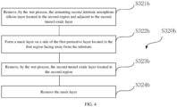
- step S3 prior to step S3, the method further includes the following step.
- a second protective layer 180 is formed on a side of the second intrinsic amorphous silicon layer 150 facing away from the substrate 110.
- the second protective layer 180 may be at least one of a silicon oxide layer, silicon oxynitride, and silicon nitride.
- the second protective layer 180 may be manufactured by a deposition method such as APCVD or PECVD.
- the second protective layer 180 is formed on the side of the second intrinsic amorphous silicon layer 150 facing away from the substrate 110, which can play a protective and blocking role in the subsequent manufacturing process.
- a thickness of the second protective layer 180 ranges from 50 nm to 100 nm.
- step S3 specifically includes the following steps.
- the second protective layer 180 and part of the second intrinsic amorphous silicon layer 150 facing away from the second tunnel oxide layer 140 that are located in the second region 112b are removed by laser.
- the remaining second intrinsic amorphous silicon layer 150 located in the second region 112b and adjacent to the second tunnel oxide layer 140 and the second tunnel oxide layer 140 located in the second region 112b are removed by a wet process.
- the second protective layer 180 and part of the second intrinsic amorphous silicon layer 150 facing away from the second tunnel oxide layer 140 that are located in the second region 112b are removed by laser; and the remaining second intrinsic amorphous silicon layer 150 and the second tunnel oxide layer 140 located in the second region 112b are removed by the wet process.
- the second intrinsic amorphous silicon layer 150 serves as a sacrificial layer and can absorb laser energy
- the second tunnel oxide layer 140 can serve as a barrier layer, which can block transmission of laser energy and reduce damage of the laser to the first intrinsic amorphous silicon layer 130.
- the remaining second intrinsic amorphous silicon layer 150 and the second tunnel oxide layer 140 are removed by the wet process, which can prevent damage to the first intrinsic amorphous silicon layer 130, thereby ensuring performance of the third doped layer 150a obtained by doping and improving efficiency of the cell.
- step S320b specifically includes the following steps.
- the remaining second intrinsic amorphous silicon layer 150 located in the second region 112b and adjacent to the second tunnel oxide layer 140 are removed by the wet process.
- the remaining second intrinsic amorphous silicon layer 150 located in the second region 112b and adjacent to the second tunnel oxide layer 140 may be removed by a polishing additive.
- the polishing additive may not cause damage to the second protective layer 180 and the second tunnel oxide layer 140, thereby preventing damage of the polishing additive to the first intrinsic amorphous silicon layer 130.
- a mask layer is formed on a side of the second protective layer 180 located in the first region 112a facing away from the substrate 110.
- the mask layer may be a photoresist layer.
- the mask layer may protect the second protective layer 180 when the second tunnel oxide layer 140 located in the second region 112b is removed, ensuring no damage to the second protective layer 180, to facilitate subsequent diffusion.
- the second tunnel oxide layer 140 located in the second region 112b is removed by the wet process.
- the second tunnel oxide layer 140 may be removed by an acid solution.
- the second tunnel oxide layer 140 may be removed by a hydrogen fluoride solution.
- a thickness of the second protective layer 180 may range from 50 nm to 100 nm, a thickness of the second tunnel oxide layer 140 may range from 1 nm to 2 nm, and the thickness of the second protective layer 180 is greater than the thickness of the second tunnel oxide layer 140. If an etching process permits, there is no need to form the mask layer on the side of the second protective layer 180 located in the first region facing away from the substrate. By controlling parameters of the etching process, when the second tunnel oxide layer 140 located in the second region is removed, the damage to the second protective layer 180 is reduced as much as possible.
- step S4 specifically includes:
- the second protective layer 180 plays a blocking role to prevent diffusion of the second element to the first intrinsic amorphous silicon layer 130 and the second intrinsic amorphous silicon layer 150 located in the first region 112a.
- the third protective layer is formed on the side of the third doped layer 150a facing away from the substrate 110, and the third protection layer may play a blocking role, which can prevent diffusion of the first element to the third doped layer 150a, thereby ensuring that doping types of the first doped layer 130a and the second doped layer 130b are the same.
- the doping types of the first doped layer 130a and the second doped layer 130b are different from a doping type of the third doped layer 150a, ensuring the passivation effect of the passivation contact structure formed on the substrate 110.
- the third protective layer may be at least one of a silicon oxide layer, silicon oxynitride, and silicon nitride.
- the second protective layer 180 may be manufactured by a deposition method such as APCVD or PECVD.
- the method further includes removing the third protective layer.
- the third protective layer may be removed by the wet process.
- step S5 the method further includes:
- first passivation antireflection layer 200a on the side of the second doped layer 130b and the third doped layer 150a facing away from the substrate 100, the first passivation antireflection layer 200a covering at least a surface on the side of the second doped layer 130b and the third doped layer 150a facing away from the substrate 100; and forming a second passivation antireflection layer 200b on the first surface of the substrate 110.
- both the first passivation antireflection layer 200a and the second passivation antireflection layer 200b may be at least one of aluminum oxide, silicon nitride, silicon oxide, gallium oxide, aluminum nitride, and silicon oxynitride.
- the first passivation antireflection layer 200a and the second passivation antireflection layer 200b may be formed simultaneously.
- the method further includes:
- thicknesses of the first tunnel oxide layer 120 and the second tunnel oxide layer 140 both range from 1 nm to 2 nm; and thicknesses of the first doped layer 130a, the second doped layer 130b, and the third doped layer 150a all range from 50 nm to 500 nm.
- an embodiment of a second aspect of the present application provides a solar cell, including:
- the solar cell in the embodiments of the present application may be manufactured with the manufacturing method, which may lead to low cell manufacturing costs, facilitate mass production of the cell, and reduce mass production costs of the cell.
- doping concentration of the first doped layer 130a may be less than doping concentration of the second doped layer 130b, thereby reducing parasitic absorption of light by the first doped layer 130a, improving efficiency of the cell, improving an ohmic contact effect between the second doped layer 130b and the electrodes, and improving efficiency and reliability of the cell.
- the second tunnel oxide layer 140 can reduce recombination, and at the same time, the second tunnel oxide layer 140 has a certain reflection effect on light, thereby improving light utilization and further improving the efficiency of the cell.
- the isolation structure 190 includes an isolation groove, the isolation groove runs through the first tunnel oxide layer 120, the first doped layer 130a, the second tunnel oxide layer 140, the second doped layer 130b, and the third doped layer 150a along a first direction X, and the first direction X is perpendicular to a plane where the substrate 110 is located.
- the first tunnel oxide layer 120 located in the first region 112a can be isolated from the first tunnel oxide layer 120 located in the second region 112b
- the first doped layer 130a and the second doped layer 130b located in the first region 112a can be isolated from the third doped layer 150a located in the second region 112b, so as to prevent recombination and improve efficiency of the cell.
- An embodiment of a third aspect of the present application provides a photovoltaic module, including the solar cell described in any one of the above embodiments in the second aspect, thereby improving efficiency of the photovoltaic module.
- An embodiment of a fourth aspect of the present application provides a photovoltaic system, including the photovoltaic module described in any one of the above embodiments in the third aspect, thereby improving efficiency of the photovoltaic module.
Landscapes
- Photovoltaic Devices (AREA)
- Life Sciences & Earth Sciences (AREA)
- Sustainable Development (AREA)
Applications Claiming Priority (1)
| Application Number | Priority Date | Filing Date | Title |
|---|---|---|---|
| CN202311078019.3A CN116825901B (zh) | 2023-08-25 | 2023-08-25 | 太阳能电池及其制备方法、光伏组件以及光伏系统 |
Publications (2)
| Publication Number | Publication Date |
|---|---|
| EP4407696A2 true EP4407696A2 (de) | 2024-07-31 |
| EP4407696A3 EP4407696A3 (de) | 2025-03-05 |
Family
ID=88116966
Family Applications (1)
| Application Number | Title | Priority Date | Filing Date |
|---|---|---|---|
| EP24182030.7A Pending EP4407696A3 (de) | 2023-08-25 | 2024-06-13 | Solarzelle und herstellungsverfahren dafür, fotovoltaisches modul und fotovoltaisches system |
Country Status (4)
| Country | Link |
|---|---|
| US (2) | US12349498B2 (de) |
| EP (1) | EP4407696A3 (de) |
| JP (1) | JP7710073B2 (de) |
| CN (1) | CN116825901B (de) |
Cited By (1)
| Publication number | Priority date | Publication date | Assignee | Title |
|---|---|---|---|---|
| CN118825141A (zh) * | 2024-09-18 | 2024-10-22 | 横店集团东磁股份有限公司 | 一种无掩膜单次沉积硅层制备tbc太阳能电池的方法 |
Families Citing this family (9)
| Publication number | Priority date | Publication date | Assignee | Title |
|---|---|---|---|---|
| CN117476780B (zh) * | 2023-12-28 | 2024-03-08 | 淮安捷泰新能源科技有限公司 | 光伏组件及其tbc太阳能电池、tbc电池的背面结构与制备 |
| CN117497645B (zh) * | 2024-01-03 | 2024-03-26 | 淮安捷泰新能源科技有限公司 | Tbc太阳能电池的制备方法、tbc太阳能电池与光伏系统 |
| CN118507573A (zh) * | 2024-01-29 | 2024-08-16 | 天合光能股份有限公司 | 太阳电池及其制备方法、光伏组件、光伏系统 |
| CN118431349B (zh) * | 2024-04-26 | 2025-06-13 | 天合光能股份有限公司 | 背接触异质结电池的制备方法 |
| CN118507548B (zh) * | 2024-07-22 | 2024-11-08 | 润马光能科技(金华)有限公司 | 光伏电池及其制备方法、光伏组件 |
| CN118676264A (zh) * | 2024-08-22 | 2024-09-20 | 天合光能股份有限公司 | 光伏电池的制备方法及光伏电池 |
| CN119767834A (zh) * | 2024-11-28 | 2025-04-04 | 天合光能股份有限公司 | 太阳能电池及其制备方法、光伏组件 |
| CN119653870B (zh) * | 2025-02-17 | 2025-04-29 | 绵阳炘皓新能源科技有限公司 | 一种自形成gap区域的TBC电池结构及其PVD法制备方法 |
| CN120091650B (zh) * | 2025-05-06 | 2025-11-07 | 浙江晶科能源有限公司 | 背接触光伏电池及其制备方法、电池组件 |
Family Cites Families (26)
| Publication number | Priority date | Publication date | Assignee | Title |
|---|---|---|---|---|
| JP3998619B2 (ja) * | 2003-09-24 | 2007-10-31 | 三洋電機株式会社 | 光起電力素子およびその製造方法 |
| US7737357B2 (en) * | 2006-05-04 | 2010-06-15 | Sunpower Corporation | Solar cell having doped semiconductor heterojunction contacts |
| US8686283B2 (en) | 2010-05-04 | 2014-04-01 | Silevo, Inc. | Solar cell with oxide tunneling junctions |
| US9054255B2 (en) * | 2012-03-23 | 2015-06-09 | Sunpower Corporation | Solar cell having an emitter region with wide bandgap semiconductor material |
| US9112068B2 (en) | 2012-10-05 | 2015-08-18 | International Business Machines Corporation | Laser doping of crystalline semiconductors using a dopant-containing amorphous silicon stack for dopant source and passivation |
| CN102856328B (zh) * | 2012-10-10 | 2015-06-10 | 友达光电股份有限公司 | 太阳能电池及其制作方法 |
| KR101622089B1 (ko) * | 2013-07-05 | 2016-05-18 | 엘지전자 주식회사 | 태양 전지 및 이의 제조 방법 |
| US9401450B2 (en) * | 2013-12-09 | 2016-07-26 | Sunpower Corporation | Solar cell emitter region fabrication using ion implantation |
| CN103985778B (zh) | 2014-05-21 | 2016-01-20 | 常州天合光能有限公司 | 具有选择性发射极的异质结太阳能电池及其制备方法 |
| CN104134707B (zh) | 2014-08-11 | 2016-05-25 | 常州天合光能有限公司 | 有利于减少正面栅线数目的异质结电池及其制备方法 |
| US9525083B2 (en) * | 2015-03-27 | 2016-12-20 | Sunpower Corporation | Solar cell emitter region fabrication with differentiated P-type and N-type architectures and incorporating a multi-purpose passivation and contact layer |
| EP3182468B1 (de) | 2015-12-18 | 2025-10-29 | JingAo Solar Co., Ltd. | Verfahren zur herstellung einer solarzelle |
| CN106328735A (zh) | 2016-11-15 | 2017-01-11 | 江南大学 | 一种c‑Si/a‑Si/mc‑Si太阳电池结构及其制备方法 |
| CN207233747U (zh) | 2017-05-31 | 2018-04-13 | 国家电投集团科学技术研究院有限公司 | 硅异质结太阳电池 |
| CN110600577A (zh) | 2018-06-12 | 2019-12-20 | 君泰创新(北京)科技有限公司 | 一种异质结太阳能电池及其制备方法 |
| CN120076466A (zh) * | 2018-09-28 | 2025-05-30 | 迈可晟太阳能有限公司 | 具有包括差异化p型和n型区域的混合架构的太阳能电池 |
| JP7458834B2 (ja) * | 2020-03-12 | 2024-04-01 | 株式会社カネカ | 太陽電池および太陽電池の製造方法 |
| CN111463306B (zh) | 2020-05-06 | 2025-05-30 | 晋能光伏技术有限责任公司 | 一种新型异质结电池及其制备方法 |
| CN113964216B (zh) * | 2021-09-22 | 2023-10-27 | 泰州隆基乐叶光伏科技有限公司 | 一种背接触电池及其制作方法 |
| CN113921625B (zh) * | 2021-09-30 | 2023-10-27 | 泰州隆基乐叶光伏科技有限公司 | 一种背接触电池及其制作方法 |
| CN116417522A (zh) * | 2021-12-29 | 2023-07-11 | 泰州隆基乐叶光伏科技有限公司 | 一种太阳能电池及其制备方法 |
| CN115513308A (zh) * | 2022-08-31 | 2022-12-23 | 隆基绿能科技股份有限公司 | 背接触太阳能电池及其制备方法 |
| CN116190483B (zh) * | 2022-09-08 | 2024-12-31 | 隆基绿能科技股份有限公司 | 一种背接触异质结太阳能电池及其制造方法 |
| CN115832065B (zh) * | 2022-11-29 | 2025-03-07 | 隆基绿能科技股份有限公司 | 一种背接触电池及其制造方法、光伏组件 |
| CN219371038U (zh) * | 2023-03-16 | 2023-07-18 | 韩华新能源(启东)有限公司 | 一种太阳能电池背面结构及n-tbc背接触太阳能电池 |
| CN116387370A (zh) * | 2023-04-10 | 2023-07-04 | 浙江爱旭太阳能科技有限公司 | P型背接触电池结构、制作方法及太阳能电池 |
-
2023
- 2023-08-25 CN CN202311078019.3A patent/CN116825901B/zh active Active
-
2024
- 2024-06-06 JP JP2024092432A patent/JP7710073B2/ja active Active
- 2024-06-13 EP EP24182030.7A patent/EP4407696A3/de active Pending
- 2024-07-10 US US18/768,660 patent/US12349498B2/en active Active
-
2025
- 2025-05-30 US US19/224,099 patent/US20250294913A1/en active Pending
Cited By (1)
| Publication number | Priority date | Publication date | Assignee | Title |
|---|---|---|---|---|
| CN118825141A (zh) * | 2024-09-18 | 2024-10-22 | 横店集团东磁股份有限公司 | 一种无掩膜单次沉积硅层制备tbc太阳能电池的方法 |
Also Published As
| Publication number | Publication date |
|---|---|
| EP4407696A3 (de) | 2025-03-05 |
| JP7710073B2 (ja) | 2025-07-17 |
| US20240363776A1 (en) | 2024-10-31 |
| CN116825901B (zh) | 2023-11-21 |
| CN116825901A (zh) | 2023-09-29 |
| JP2024113119A (ja) | 2024-08-21 |
| US12349498B2 (en) | 2025-07-01 |
| US20250294913A1 (en) | 2025-09-18 |
Similar Documents
| Publication | Publication Date | Title |
|---|---|---|
| EP4407696A2 (de) | Solarzelle und herstellungsverfahren dafür, fotovoltaisches modul und fotovoltaisches system | |
| CN111834493B (zh) | 一种TOPCon太阳能电池的制备方法 | |
| JP7553680B2 (ja) | 太陽電池及びその製造方法、太陽光発電モジュール及び太陽光発電システム | |
| CN117637874B (zh) | 一种背接触电池及其制造方法 | |
| US20250351615A1 (en) | Solar cell and preparation method therefor | |
| EP4401150B1 (de) | Solarzelle, herstellungsverfahren dafür, fotovoltaisches modul und photovoltaiksystem | |
| KR20110118135A (ko) | 후방 접촉 슬리버 셀 | |
| US20250169221A1 (en) | Solar cell, photovoltaic module, and photovoltaic system | |
| US20230327030A1 (en) | Solar cell and preparation method thereof | |
| JP2024113125A (ja) | 太陽電池及びその製造方法、太陽光発電モジュール、太陽光発電システム | |
| US20160072003A1 (en) | Manufacturing method of solar cell | |
| CN119767836A (zh) | 背接触太阳能电池及其制作方法 | |
| US20230253521A1 (en) | Solar cell manufacture | |
| US20230253520A1 (en) | Solar cell manufacture | |
| KR20110082372A (ko) | 태양 전지 모듈 및 이의 제조 방법 | |
| CN119170665A (zh) | 太阳能电池及其制作方法、光伏组件 | |
| EP4648113A1 (de) | Interdigitale rückkontaktsolarzelle und herstellungsverfahren dafür | |
| TW201635565A (zh) | 背接觸太陽能電池組及其製造方法 | |
| KR20180064194A (ko) | 태양 전지 제조 방법 | |
| US20250228036A1 (en) | Back-contact solar cell | |
| CN117790600B (zh) | 背接触太阳能电池的制备方法 | |
| CN119997655B (zh) | 一种太阳能电池的制备方法及太阳能电池 | |
| CN119767796A (zh) | 太阳能电池及其制备方法、光伏组件 | |
| CN120035265A (zh) | 背接触电池及其制备方法 | |
| CN120239359A (zh) | 背接触电池及其制备方法 |
Legal Events
| Date | Code | Title | Description |
|---|---|---|---|
| PUAI | Public reference made under article 153(3) epc to a published international application that has entered the european phase |
Free format text: ORIGINAL CODE: 0009012 |
|
| STAA | Information on the status of an ep patent application or granted ep patent |
Free format text: STATUS: REQUEST FOR EXAMINATION WAS MADE |
|
| 17P | Request for examination filed |
Effective date: 20240613 |
|
| AK | Designated contracting states |
Kind code of ref document: A2 Designated state(s): AL AT BE BG CH CY CZ DE DK EE ES FI FR GB GR HR HU IE IS IT LI LT LU LV MC ME MK MT NL NO PL PT RO RS SE SI SK SM TR |
|
| REG | Reference to a national code |
Ref country code: DE Ref legal event code: R079 Free format text: PREVIOUS MAIN CLASS: H01L0031180000 Ipc: H10F0010166000 |
|
| PUAL | Search report despatched |
Free format text: ORIGINAL CODE: 0009013 |
|
| AK | Designated contracting states |
Kind code of ref document: A3 Designated state(s): AL AT BE BG CH CY CZ DE DK EE ES FI FR GB GR HR HU IE IS IT LI LT LU LV MC ME MK MT NL NO PL PT RO RS SE SI SK SM TR |
|
| RIC1 | Information provided on ipc code assigned before grant |
Ipc: H10F 77/30 20250101ALI20250127BHEP Ipc: H10F 71/00 20250101ALI20250127BHEP Ipc: H10F 77/20 20250101ALI20250127BHEP Ipc: H10F 10/166 20250101AFI20250127BHEP |