EP4407678A1 - Chipteststruktur und chiptestverfahren - Google Patents
Chipteststruktur und chiptestverfahren Download PDFInfo
- Publication number
- EP4407678A1 EP4407678A1 EP23878359.1A EP23878359A EP4407678A1 EP 4407678 A1 EP4407678 A1 EP 4407678A1 EP 23878359 A EP23878359 A EP 23878359A EP 4407678 A1 EP4407678 A1 EP 4407678A1
- Authority
- EP
- European Patent Office
- Prior art keywords
- test
- interposer
- solder balls
- test points
- potentials
- Prior art date
- Legal status (The legal status is an assumption and is not a legal conclusion. Google has not performed a legal analysis and makes no representation as to the accuracy of the status listed.)
- Pending
Links
Images


Classifications
-
- G—PHYSICS
- G01—MEASURING; TESTING
- G01R—MEASURING ELECTRIC VARIABLES; MEASURING MAGNETIC VARIABLES
- G01R31/00—Arrangements for testing electric properties; Arrangements for locating electric faults; Arrangements for electrical testing characterised by what is being tested not provided for elsewhere
- G01R31/28—Testing of electronic circuits, e.g. by signal tracer
- G01R31/2851—Testing of integrated circuits [IC]
- G01R31/2855—Environmental, reliability or burn-in testing
- G01R31/2856—Internal circuit aspects, e.g. built-in test features; Test chips; Measuring material aspects, e.g. electro migration [EM]
-
- H—ELECTRICITY
- H10—SEMICONDUCTOR DEVICES; ELECTRIC SOLID-STATE DEVICES NOT OTHERWISE PROVIDED FOR
- H10P—GENERIC PROCESSES OR APPARATUS FOR THE MANUFACTURE OR TREATMENT OF DEVICES COVERED BY CLASS H10
- H10P74/00—Testing or measuring during manufacture or treatment of wafers, substrates or devices
- H10P74/20—Testing or measuring during manufacture or treatment of wafers, substrates or devices characterised by the properties tested or measured, e.g. structural or electrical properties
- H10P74/207—Electrical properties, e.g. testing or measuring of resistance, deep levels or capacitance-voltage characteristics
-
- H—ELECTRICITY
- H10—SEMICONDUCTOR DEVICES; ELECTRIC SOLID-STATE DEVICES NOT OTHERWISE PROVIDED FOR
- H10P—GENERIC PROCESSES OR APPARATUS FOR THE MANUFACTURE OR TREATMENT OF DEVICES COVERED BY CLASS H10
- H10P74/00—Testing or measuring during manufacture or treatment of wafers, substrates or devices
- H10P74/23—Testing or measuring during manufacture or treatment of wafers, substrates or devices characterised by multiple measurements, corrections, marking or sorting processes
-
- H—ELECTRICITY
- H10—SEMICONDUCTOR DEVICES; ELECTRIC SOLID-STATE DEVICES NOT OTHERWISE PROVIDED FOR
- H10P—GENERIC PROCESSES OR APPARATUS FOR THE MANUFACTURE OR TREATMENT OF DEVICES COVERED BY CLASS H10
- H10P74/00—Testing or measuring during manufacture or treatment of wafers, substrates or devices
- H10P74/27—Structural arrangements therefor
- H10P74/273—Interconnections for measuring or testing, e.g. probe pads
-
- H—ELECTRICITY
- H10—SEMICONDUCTOR DEVICES; ELECTRIC SOLID-STATE DEVICES NOT OTHERWISE PROVIDED FOR
- H10W—GENERIC PACKAGES, INTERCONNECTIONS, CONNECTORS OR OTHER CONSTRUCTIONAL DETAILS OF DEVICES COVERED BY CLASS H10
- H10W20/00—Interconnections in chips, wafers or substrates
- H10W20/20—Interconnections within wafers or substrates, e.g. through-silicon vias [TSV]
-
- H—ELECTRICITY
- H10—SEMICONDUCTOR DEVICES; ELECTRIC SOLID-STATE DEVICES NOT OTHERWISE PROVIDED FOR
- H10W—GENERIC PACKAGES, INTERCONNECTIONS, CONNECTORS OR OTHER CONSTRUCTIONAL DETAILS OF DEVICES COVERED BY CLASS H10
- H10W42/00—Arrangements for protection of devices
- H10W42/121—Arrangements for protection of devices protecting against mechanical damage
-
- H—ELECTRICITY
- H10—SEMICONDUCTOR DEVICES; ELECTRIC SOLID-STATE DEVICES NOT OTHERWISE PROVIDED FOR
- H10W—GENERIC PACKAGES, INTERCONNECTIONS, CONNECTORS OR OTHER CONSTRUCTIONAL DETAILS OF DEVICES COVERED BY CLASS H10
- H10W70/00—Package substrates; Interposers; Redistribution layers [RDL]
- H10W70/60—Insulating or insulated package substrates; Interposers; Redistribution layers
- H10W70/62—Insulating or insulated package substrates; Interposers; Redistribution layers characterised by their interconnections
- H10W70/63—Vias, e.g. via plugs
- H10W70/635—Through-vias
-
- H—ELECTRICITY
- H10—SEMICONDUCTOR DEVICES; ELECTRIC SOLID-STATE DEVICES NOT OTHERWISE PROVIDED FOR
- H10P—GENERIC PROCESSES OR APPARATUS FOR THE MANUFACTURE OR TREATMENT OF DEVICES COVERED BY CLASS H10
- H10P74/00—Testing or measuring during manufacture or treatment of wafers, substrates or devices
- H10P74/27—Structural arrangements therefor
- H10P74/277—Circuits for electrically characterising or monitoring manufacturing processes, e.g. circuits in tested chips or circuits in testing wafers
-
- H—ELECTRICITY
- H10—SEMICONDUCTOR DEVICES; ELECTRIC SOLID-STATE DEVICES NOT OTHERWISE PROVIDED FOR
- H10W—GENERIC PACKAGES, INTERCONNECTIONS, CONNECTORS OR OTHER CONSTRUCTIONAL DETAILS OF DEVICES COVERED BY CLASS H10
- H10W70/00—Package substrates; Interposers; Redistribution layers [RDL]
- H10W70/60—Insulating or insulated package substrates; Interposers; Redistribution layers
- H10W70/67—Insulating or insulated package substrates; Interposers; Redistribution layers characterised by their insulating layers or insulating parts
- H10W70/68—Shapes or dispositions thereof
- H10W70/685—Shapes or dispositions thereof comprising multiple insulating layers
-
- H—ELECTRICITY
- H10—SEMICONDUCTOR DEVICES; ELECTRIC SOLID-STATE DEVICES NOT OTHERWISE PROVIDED FOR
- H10W—GENERIC PACKAGES, INTERCONNECTIONS, CONNECTORS OR OTHER CONSTRUCTIONAL DETAILS OF DEVICES COVERED BY CLASS H10
- H10W72/00—Interconnections or connectors in packages
- H10W72/90—Bond pads, in general
- H10W72/921—Structures or relative sizes of bond pads
- H10W72/923—Bond pads having multiple stacked layers
- H10W72/9232—Bond pads having multiple stacked layers with additional elements interposed between layers
-
- H—ELECTRICITY
- H10—SEMICONDUCTOR DEVICES; ELECTRIC SOLID-STATE DEVICES NOT OTHERWISE PROVIDED FOR
- H10W—GENERIC PACKAGES, INTERCONNECTIONS, CONNECTORS OR OTHER CONSTRUCTIONAL DETAILS OF DEVICES COVERED BY CLASS H10
- H10W90/00—Package configurations
- H10W90/701—Package configurations characterised by the relative positions of pads or connectors relative to package parts
- H10W90/721—Package configurations characterised by the relative positions of pads or connectors relative to package parts of bump connectors
- H10W90/724—Package configurations characterised by the relative positions of pads or connectors relative to package parts of bump connectors between a chip and a stacked insulating package substrate, interposer or RDL
Definitions
- the embodiments of the present disclosure relate to a chip testing structure and a chip testing method.
- the manufacturing process of a chip is mainly divided into several steps: wafer fabrication, packaging, and test.
- the interposer has a certain stress effect, easily causing the interposer to be fragmented or have a crack in the chip packaging process, and causing a poor quality of the packaged chip.
- the embodiments of the present disclosure provide a chip testing structure and a chip testing method, which can accurately and efficiently determine whether an interposer is fragmented or has a crack, implementing the test for the interposer in the whole process of the packaging.
- the embodiments of the present disclosure provide a chip testing structure, which includes: an interposer, a plurality of chips on the interposer, and a plurality of test points on the interposer.
- the plurality of the test points are connected in series, an electrical connecting wire of the plurality of the test points is provided in an interposer wiring layer of the interposer, and an electrical connecting wire of adjacent test potentials includes a plurality of sub-connecting wires, different sub-connecting wires are positioned at different heights of the interposer wiring layer, and the plurality of the sub-connecting wires are connected sequentially based on the height of the interposer wiring layer.
- the test potentials of the plurality of the test points indicate an open circuit connection, the interposer is indicated to be fragmented or have a crack.
- the sub-connecting wires of the plurality of the test points are displayed as a serpentine shape on a cross-section of the interposer according to a wiring distribution sequence of the interposer wiring layer.
- the plurality of the test points at least include the first test point, the second test point, and the third test point.
- the position interval between the first test point and the second test point on the interposer is the first value
- the position interval between the first test point and the third test point on the interposer is the second value
- the position interval between the second test point and the third test point on the interposer is the third value.
- the second value and the third value are determined based on the first value, and the second value is equal to the third value.
- the third test point is determined as the first test point or the second test point.
- the first test point and the second test point are respectively positioned at a start point and an end point, and the first value is a maximum value of the position interval on the interposer.
- the interposer wiring layer includes the first intermediate layer and the second intermediate layer bonded below the first intermediate layer, and an electrical connecting wire of the first intermediate layer is in communication with an electrical connecting wire of the second intermediate layer.
- the bonding quality of the first intermediate layer and the second intermediate layer is determined according to the test potentials of the plurality of the test points.
- a plurality of sub-connecting wires of corresponding test points constitute a comb-shaped short-circuit measurement structure, and a comb-shaped short-circuit measurement structure between adjacent test points is in open-circuit connection.
- the test potentials of the plurality of the test points indicate a short-circuit connection
- the plurality of the test points are indicated to be short-connected at front of the interposer.
- the serpentine open-circuit measurement structure with stacked through vias is correspondingly provided between adj acent test points.
- the test potentials of the plurality of the test points indicate the open circuit connection
- the plurality of the test points are indicated to be open-connected at the front of the interposer.
- a plurality of through-vias electrodes electrically connected with the test points are provided on the interposer, and a plurality of interconnection structures through the chips are provided on the chips.
- the chips are bonded to the interposer, a bottom of the interconnection structures is electrically connected with the through-vias electrodes, and a top of the interconnection structures is provided with interconnection solder balls.
- test potentials of the interconnecting solder balls electrically connected with the test points indicate a preset potential
- the interconnecting solder balls are indicated to be electrically connected with the interconnection structures.
- solder balls at two ends of a chip circuit structure are served as circuit testing solder balls, a chip circuit testing structure is provided between the circuit testing solder balls, the chip circuit testing structure is configured to electrically connect the circuit testing solder balls, and when test potentials of test points electrically connected with the circuit testing solder balls indicate the open circuit connection, the chip circuit structure is indicated to be damaged.
- interposer solder balls are provided on through-vias electrodes at a side of the interposer away from the chips, an interposer solder ball testing structure is provided on solder balls of the through-vias electrodes that are provided with the interposer solder balls, the interposer solder balls are configured for short-connecting the interposer solder ball testing structure, and when a test voltage is applied to the interposer solder balls, and test potentials between the interposer solder balls indicate that the interposer solder balls are short-connected, the interposer solder balls are indicated to be electrically connected with the through-vias electrodes.
- the chip testing structure further comprises a substrate.
- An interposer structure and bottom solder balls at bottom of the interposer structure are provided in the substrate, and the interposer is connected with the interposer structure of the substrate to the bottom solder balls based on the interposer solder balls.
- the bottom solder balls are indicated to be electrically connected with the chips.
- the bottom solder balls are indicated to be electrically connected with the chips and the interposer.
- the embodiments of the present disclosure provide a chip testing method, which includes: providing the chip testing structure, and measuring test potentials of the plurality of the test points.
- the chip testing structure includes an interposer, a plurality of chips on the interposer, and a plurality of test points on the interposer.
- the plurality of the test points are connected in series, an electrical connecting wire of the plurality of the test points is provided in an interposer wiring layer of the interposer, and an electrical connecting wire of adj acent test potentials comprises a plurality of sub-connecting wires, different sub-connecting wires are positioned at different heights of the interposer wiring layer, and the plurality of the sub-connecting wires are connected sequentially based on the height of the interposer wiring layer.
- the interposer When the test potentials of the plurality of the test points indicate an open circuit connection, the interposer is indicated to be fragmented or have a crack.
- the measuring test potentials of the plurality of the test points includes:
- a position interval between the first test point and the second test point on the interposer is the first value.
- the third test point is determined as the first test point or the second test point, and the third test point is determined based on the first value.
- the interposer wiring layer includes the first intermediate layer and the second intermediate layer, the second intermediate layer is bonded below the first intermediate layer, and an electrical connecting wire of the first intermediate layer is in communication with an electrical connecting wire of the second intermediate layer.
- the measuring test potentials of the plurality of the test points includes: determining a bonding quality of the first intermediate layer and the second intermediate layer according to the test potentials of the plurality of the test points.
- the test points are provided with a comb-shaped short-circuit measurement structure, the comb-shaped short-circuit measurement structure corresponds to a plurality of sub-connecting wires of the test points, and a comb-shaped short-circuit measurement structure of adjacent test points is open-circuit.
- the measuring test potentials of the plurality of the test points includes: measuring the test potentials of the plurality of the test points.
- test potentials of the plurality of the test points indicate a short-circuit connection
- the plurality of the test points are indicated to be short-connected on the side of the interposer where the test points are provided.
- a serpentine open-circuit measurement structure with stacked through vias is provided between adjacent test points, and the serpentine open-circuit measurement structure with the stacked through vias corresponds to the plurality of the sub-connecting wires of the adj acent test points.
- the measuring test potentials of the plurality of the test points includes: measuring test potentials of the adjacent test points.
- test potentials of the adjacent test points indicate an open circuit connection
- the adjacent test points are indicated to be open-connected on the side of the interposer where the test points are provided.
- the chip testing method further includes: thinning the interposer, and leaking out a plurality of through-vias electrodes electrically connected with the test points.
- the chips are provided with a plurality of interconnection structures through the chips, the chips are bonded to the interposer so that a bottom of the interconnection structures is connected with the through-vias electrodes, and a top of the interconnection structures is provided with interconnection solder balls.
- the measuring test potentials of the plurality of the test points includes: applying a voltage to the test points and the interconnecting solder balls electrically connected with the test points, and measuring test potentials of the interconnecting solder balls electrically connected with the test points.
- test potentials of the interconnecting solder balls electrically connected with the test points indicate a preset potential
- the interconnecting solder balls are indicated to be electrically connected with the interconnection structures.
- the chips include circuit testing solder balls, the circuit testing solder balls are solder balls at two ends of a chip circuit structure, and a chip circuit testing structure is provided between the circuit test solder balls so as to electrically connect the circuit testing solder balls.
- the measuring test potentials of the plurality of the test points further includes: measuring the test potentials of the plurality of the test points that are electrically connected with the circuit testing solder balls.
- test potentials indicate an open circuit connection
- the chip circuit structure is indicated to be damaged.
- the chip testing method further includes:
- the measuring test potentials of the plurality of the test points further includes: applying a test voltage to the interposer solder balls, and measuring test potentials of the interposer solder balls.
- the interposer solder balls are indicated to be electrically connected with the through-vias electrodes.
- the substrate includes an interposer structure and bottom solder balls at bottom of the interposer structure, and the interposer is connected with the interposer structure of the substrate to the bottom solder balls based on the interposer solder balls.
- the measuring test potentials of the plurality of the test points further includes: applying a test voltage on the bottom solder balls to through-vias electrodes that are short-connected, and measuring test potentials between the bottom solder balls.
- the bottom solder balls are indicated to be electrically connected with the interposer.
- the measuring test potentials of the plurality of the test points further includes: applying a test voltage on the bottom solder balls to the interconnecting solder balls that are short-connected, and measuring the test potentials between the bottom solder balls.
- the bottom solder balls are indicated to be electrically connected with the chips.
- the measuring test potentials of the plurality of the test points further includes: applying a test voltage on the bottom solder balls to a short-connected circuit that is mixed-connected with the interconnecting solder balls and through-vias electrodes, and measuring the test potentials between the bottom solder balls.
- the bottom solder balls are indicated to be electrically connected with the chips and the interposer.
- the chip testing structure includes an interposer, and a plurality of chips on the interposer, and a plurality of test points on the interposer.
- the plurality of the test points are connected in series, an electrical connecting wire of the plurality of the test points is provided in an interposer wiring layer of the interposer, and an electrical connecting wire of adj acent test potentials comprises a plurality of sub-connecting wires, different sub-connecting wires are positioned at different heights of the interposer wiring layer, and the plurality of the sub-connecting wires are connected sequentially based on the height of the interposer wiring layer.
- the embodiments of the present disclosure based on the plurality of test points that are connected in series on the interposer, can accurately and efficiently determine whether the interposer is fragmented or has a crack by testing the potentials of the plurality of test points, so as to implement the detection for the interposer in the whole process of the packaging procedure.
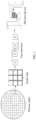
- the WAT test structure is generally set on the wafer scribe line, in schematic diagram of the test structure on the wafer as illustrated in FIG. 1 , the silicon wafer is a whole wafer product, each small grid on the silicon wafer represents a chip.
- G, D, S, B are the top metal windows, usually called the bonding PAD, and the bonding PAD is correspondingly designed with a physical layout in the scribe line.
- different test structures can form a group of test modules, and each group of test modules has a different name, so that each wafer contains many different WAT test modules.
- the packaging process has a variety of packaging technologies in the terms of implementation methods, such as flip chip, bumping, wafer-level packaging, 2.5D packaging (CoWoS, RDL, and etc.), 3D packaging (TSV), and etc.
- the CoWoS (chip-on-wafer-on-substrate) packaging technology in 2.5D packaging is taken as an example to illustrate the chip packaging process.
- the chip packaging based on the high fine-pitch wiring capability of the interposer, the chip can be stacked with a wafer through the interposer, in which the connection part between the chip and the interposer is called the ubump, and the ubump is formed of a pair of metal leads with a solder welded in the middle, and then the filler is filled to protect the chip and the connected structure to form a CoW (chip-on-wafer) wafer.
- the CoW wafer is connected to the carrier board and are polished chemically and mechanically, the interposer is thinned to expose the through-silicon vias (TSVs), and then the wiring is performed and solder balls are soldered according to the exposed through-silicon vias.
- TSVs through-silicon vias
- the CoW wafer is transferred from the carrier board to the tape, and the chip is obtained by cutting the wafer, and the chip is taken off from the tape and flip-chip mounted on the substrate to form the CoWoS structure.
- a protection structure is added and the thermal interface metal is used to fill the gap between the protective cover and the chip, therefore, the chip packaging is completed.
- the designed integrated circuit is projected onto the interposer. Because the size of the mask is fixed, for example, the size is 26mm*33mm, and the area of the interposer is larger, thus the illumination splicing on the interposer is required to lithography the integrated circuit onto an interposer having a larger area. However, the quality of the splicing area on the interposer is difficult to test, resulting in the quality problem in the packaged chip. In addition, in the process of packaging, a bonding connection between the interposer and the substrate exists, making the overall stress risk corresponding to the interposer high, also causing the interposer to be fragmented or have a crack, and causing a poor quality of the packaged chip. Therefore, the interposer is required to be tested during the whole process of packaging, in order to determine whether the interposer is fragmented or has a crack, thereby quickly locating the problem point.
- the embodiments of this company provide a new chip testing structure, which includes an interposer, a plurality of chips on the interposer, and a plurality of test points on the interposer.
- the plurality of the test points are connected in series, an electrical connecting wire of the plurality of the test points is provided in an interposer wiring layer of the interposer, and an electrical connecting wire of adjacent test potentials includes a plurality of sub-connecting wires, different sub-connecting wires are positioned at different heights of the interposer wiring layer, and the plurality of the sub-connecting wires are connected sequentially based on the height of the interposer wiring layer.
- the test potentials of the plurality of the test points indicate an open circuit connection, the interposer is indicated to be fragmented or have a crack.
- the embodiment of the present disclosure based on the plurality of test points connected in series on the interposer, and by testing the potentials of the plurality of test points, can accurately and efficiently determine whether the interposer is fragmented or has a crack, so as to implement the detection for the interposer in the whole process of packaging.
- the detection for the interposer can be implemented by monitoring the electrical characteristic parameters during the chip packaging process and monitoring the connectivity of the various components.
- the wafer is required to be cut in the packaging process, and the test structure provided on the wafer scribe line may be cut off, thus, based on the test structure provided on the wafer scribe line, the detection for the interposer is difficult to be implemented in the whole process of packaging, and then the problem point is difficult to be located.
- the front side test for the interposer cannot be implemented.
- the location of the problem point can be implemented based on the plurality of test points positioned on the interposer. While, the test for the bumps of the interposer is implemented based on the electrical connection wires corresponding to the plurality of test points that are provided in the interposer wiring layer, and the front test for the interposer is implemented based on the test structure corresponding to the plurality of test points.
- FIG. 2 illustratively illustrates a top-down schematic diagram of a chip testing structure provided by the embodiment of the present disclosure.
- the chip testing structure includes: an interposer 10, a plurality of chips 20 positioned on the interposer, and a plurality of test points 30 positioned on the interposer.
- the interposer 10 serves as a packaging carrier, which is a core structure in the chip packaging process, and provides the electrical connection, protection, support, and heat dissipation for the chips.
- the interposer may be e.g., a silicon interposer.
- through silicon vias TSV may be provided on the interposer to implement the interconnection of the chips, the wafer, etc.
- the plurality of chips 20 may be set according to the design requirements, and FIG. 2 is illustrated by only taking the high-bandwidth memory (HBM) and the system-on-chip (SOC) as an example.
- the plurality of chips 20 may further be chips such as GPUs, etc.
- the plurality of test points 30 may be understood as a metal window of the WAT test structure (WAT-PAD), which evenly surrounds the edge of the interposer.
- WAT-PAD WAT test structure
- the plurality of test points in the embodiments of the present disclosure are connected in series, and the electrical connecting wire of the plurality of test points is provided in the interposer wiring layer of the interposer, and the electrical connecting wire of adjacent test potentials includes a plurality of sub-connecting wires, and the different sub-connecting wires are positioned at different heights of the interposer wiring layers, and the plurality of sub-connecting wires are connected sequentially based on the height of the interposer wiring layer.
- the plurality of test points in the embodiments of the present disclosure are positioned on the interposer, and the electrical connecting wire of the plurality of test points is provided on the interposer wiring layer, so that the plurality of test points can be avoided from being cut off during the cutting process of the wafer, and then in the whole process of packaging of the chip, the plurality of test points can be used to test and monitor the interposer. Because the plurality of test points are evenly distributed in a circle of the edge of the interposer, the electrical characteristic parameters in the chip packaging process and the connectivity of various components can be monitored based on the plurality of test points provided. Therefore, when the test potentials of the plurality of test points indicate an open circuit connection, the interposer is indicated to be fragmented or have cracks, implementing an accurate and efficient location of problem points in the process development.
- the embodiments of the present disclosure based on the plurality of test points that are connected in series on the interposer, can accurately and efficiently determine whether the interposer is fragmented or has a crack by testing the potentials of the plurality of test points, so as to implement the detection for the interposer in the whole process of the packaging procedure.
- FIG. 3 illustratively illustrates a cross-sectional schematic diagram of a chip testing structure provided by the embodiment of the present disclosure.
- 1 , 2, 3 and 4 are the plurality of different test points.
- the distribution positions of the test points 1, 2, 3 may be a side corresponding to the long edge of the interposer
- the distribution position of the test point 4 may be a side corresponding to the short edge of the interposer
- the connecting wires with different thicknesses in FIG. 3 are sub-connecting wires of the test points.
- the interposer wiring layer of the interposer may be distributed in a plurality of layers, and the sub-connecting wires with the same thickness in FIG. 3 are on the same layer of the interposer wiring layer of the interposer.
- the black box points are the connecting points of the sub-connecting wires positioned in different layers. It can be seen that the sub-connecting wires of the plurality of test points in the embodiment of the present application are connected in a serpentine shape on the cross-section of the interposer according to the wiring distribution sequence of the interposer wiring layer, so that the test potentials of the plurality of test points can characterize the state of the interposer being fragmented or having cracks.
- the interposer In the process of packaging, for example, before completing the CoW process, the interposer needs to be tested for quality, so as to detect whether the interposer having a splicing area is fragmented or has cracks.
- an open-circuit and/or short-circuit test can be performed on the plurality of test points, so as to determine whether the interposer having a splicing area is fragmented or has cracks.
- the plurality of test points may at least include the first test point, the second test point, and the third test point.
- the position interval between the first test point and the second test point on the interposer is the first value
- the position interval between the first test point and the third test point on the interposer is the second value
- the position interval between the second test point and the third test point on the interposer is the third value.
- the second value and the third value are determined based on the first value, and the second value is equal to the third value.
- the third test point is determined as the first test point or the second test point.
- the quality test for the interposer may be performed in various steps of the chip packaging process, so as to ensure that the interposer entering into respective processe is a qualified interposer. Therefore, the timing of the quality test for the interposer is not limited by the embodiments of the present disclosure.
- the first test point and the second test point may be positioned at the starting point and the end point respectively, and the first value is the maximum value of the position intervals on the interposer.
- test points illustrated in FIG. 3 are taken as an example to describe.
- test point 1 and the test point 4 When the test point 1 and the test point 4 are tested, in response to the test potential indicate the open circuit, it indicates that the fragmentation or crack of the interposer may exist from the position of the interposer corresponding to the test point 1 to the position of the interposer corresponding to the test point 4, so that new test points may be determined again by taking half of the path based on the position interval between the test point 1 and the test point 4, and the quality test is performed again.
- the new test points may be determined as the test point 2 and the test point 3.
- the test potential between the test point 1 and the test point 2 and the test potential between the test point 3 and the test point 4 may be tested respectively.
- the plurality of test points on the interposer when the plurality of test points on the interposer are designed, different test points may be evenly distributed at the edge position of the interposer, so as to perform the quality test for the interposer.
- the plurality of test points may also be designed inside the interposer, which is not limited by the embodiments of the present disclosure, and the distribution position of the test points can be placed correspondingly according to the design requirements.
- FIG. 4 illustrates an optional structural schematic diagram of the interposer of the embodiment of the present disclosure.
- the interposer 10 may be constituted by a stacking structure, and the interposer 10 includes: the first intermediate layer 11 and the second intermediate layer 12 stacked below the first intermediate layer 11.
- the first intermediate layer and the second intermediate layer may be stacked by hybrid bonding 13.
- the electrical connecting wires of the first intermediate layer may be in communication with the electrical connecting wires of the second intermediate layer through the hybrid bonding 13.
- the bonding quality of the first intermediate layer and second intermediate layer can be determined according to the test potentials of the plurality of test points on the interposer. In an optional example, in response to the test potentials of the plurality of test points indicating the open-circuit connection, then the corresponding bonding quality between the first intermediate layer and second intermediate layer is indicated to be unqualified.
- test point 1 and the test point 3 are tested, and in response to the test potential indicating the open circuit, the bonding quality of the part corresponding to the test point 1 and the test point 3 of the interposer in the stacked configuration is poor, and then the test is repeated based on the above-mentioned method of re-determining the test points, which can accurately determine the bonding point that does not reach the standard in the interposer constituting the stacked configuration.
- the front of the interposer is provided with a conventional open and short circuit testing structure, and the conventional open and short circuit testing structure may be provided below or around the test points according to the design requirements.
- FIG. 5 illustrates an optional schematic diagram of an open and short circuit testing structure corresponding to the test points.
- the open and short circuit testing structure may be constituted by a plurality of sub-connecting wires based on the test points.
- the plurality of sub-connecting wires corresponding to the test points may constitute a comb-shaped short-circuit measurement structure (as indicated by the number 51 in the figure), and the comb-shaped short-circuit measurement structure between adjacent test points is in the open-circuit connection.
- a serpentine open-circuit measurement structure with stacked through vias may be correspondingly provided between adjacent test points.
- the open and short circuit testing structure of the test point in response to the test potentials of the plurality of test points indicate the open-circuit connection, the plurality of test points are indicated to be open-connected at the front of the interposer.
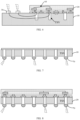
- the interposer may be provided with a plurality of through-vias electrodes electrically connected with the plurality of test points, and the chip may be provided with a plurality of interconnection structures through the chip.
- the TSV represents through vias on the interposer, and the position circled by dotted lines is the interconnection structure of the chip. Referring to FIG. 6 , the chip is bonded to the interposer, the bottom of the interconnection structure is connected with the through-vias electrodes, and the top of the interconnection structure may be provided with interconnect solder balls (as illustrated as the circles in FIG. 6 ).
- the test potentials of the interconnection solder balls electrically connected to the test points may indicate a preset potential, the interconnection solder balls are indicated to be electrically connected with the interconnection structure.
- the preset potential may be a pre-set potential range, such as a voltage range of 1V ⁇ 2V.
- the interposer is bonded with chips, etc., and the overall stress risk is high.
- a frontal interconnection test is required to be performed on the CoW wafer, so as to determine the bonding interconnection quality of the chip. Therefore, based on the structure as illustrated in FIG. 6 , the test for the bonding interconnection quality of the ubumps can be implemented by using a Kelvin four-terminal test method, so as to determine the electrical connection performance of the interconnection structure of the interconnection solder balls and the chip, and the electrical connection performance includes such as a virtual connection, a short connection, and etc.
- the solder balls at two ends of the chip circuit structure may be served as circuit testing solder balls, and the chip circuit testing structure (as indicated by the number 60 illustrated in FIG. 6 ) may be provided between the circuit testing solder balls, wherein the chip circuit testing structure is configured for electrically connecting with the circuit testing solder balls.
- the chip circuit structure is indicated to be damaged.
- test points of the interposer can be used to retest whether a fragmentation or crack of the interposer is caused in the chip packaging process, so as to determine whether the stress in the chip packaging process causes an effect on the interposer.
- FIG. 7 illustratively illustrates another optional schematic diagram of a chip testing structure.
- interposer solder balls as indicated by the number 70 in the figure
- an interposer solder ball testing structure is provided on the solder balls of the through-vias electrodes where the interposer solder balls are provided.
- the interposer solder balls are configured to be short-connected with the interposer solder ball testing structure, and when a test voltage is applied to the interposer solder balls, and the test potentials between the interposer solder balls indicate that the interposer solder balls are short-connected, the interposer solder balls are indicated to be electrically connected to the through-vias electrodes.
- FIG. 8 illustratively illustrates another optional schematic diagram of the chip testing structure.
- the test principle of testing the electrical connection between the interposer solder balls and the through-vias electrodes may be used, and when the chip has a chip circuit structure, whether the stress causes an effect on the bonding of the chip during the chip packaging process is determined by using interposer solder balls to test the bonding quality of the hybrid bonding and through-vias electrodes that implement the bonding.
- a chip is required to be installed on a substrate to obtain a complete chip after packaging, and then a chip testing structure may further include a substrate.
- FIG. 9 illustratively illustrates another optional schematic diagram of a chip testing structure.
- the substrate 90 is provided with an interposer structure (the position circled by dotted lines in the figure) and bottom solder balls (as indicated by the number 91 in the figure) positioned at the bottom of the interposer structure, and the interposer may be connected to the bottom solder balls based on the interposer solder balls and the interposer structure of the substrate.
- a test voltage may be applied to the bottom solder balls to the through-vias electrodes that are short-connected.
- the bottom solder balls are indicated to be electrically connected with the interposer.
- the applied test voltage may be transmitted based on the path, that is, there is no possibility of being fragmented or having a crack for the interposer bonded with the substrate t, i.e., the interposer is not damaged by the overall stress during the chip packaging process.
- a test voltage may be applied to the bottom solder balls to interconnection solder balls that are short-connected.
- the bottom solder balls are indicated to be electrically connected with the chip.
- the applied test voltage may be transmitted based on the path, i.e., the chip bonded with the interposer is not damaged during the packaging process.
- a test voltage may be applied to the bottom solder balls to a short-connected circuit that is mixed-connected with the interconnecting solder balls and through-vias electrodes.
- the bottom solder balls are indicated to be electrically connected with the chip and the interposer.
- the applied test voltage may be transmitted based on the path, that is, the electrical connection function of the chip after packaging is not damaged, and the quality of the chip after packaging satisfies the standard.
- the embodiments of the present disclosure based on the plurality of test points that are connected in series on the interposer, can accurately and efficiently determine whether the interposer is fragmented or has a crack by testing the potentials of the plurality of test points, so as to implement the detection for the interposer in the whole process of the packaging procedure.
- FIG. 10 illustratively illustrates an optional flowchart schematic diagram of a chip testing method. As illustrated in FIG. 10 , the following steps may be included. The content described below can be corresponded to and referred to the above description.
- Step S101 providing a chip testing structure.
- the chip testing structure may include an interposer, a plurality of chips positioned on the interposer, and a plurality of test points positioned on the interposer.
- the plurality of test points are connected in series, and the electrical connecting wires of the plurality of test points are provided in an interposer wiring layer of the interposer, and the electrical connecting wires of adjacent test potentials include a plurality of sub-connecting wires, the different sub-connecting wires are positioned at different heights of the interposer wiring layers, and the plurality of sub-connecting wires are connected sequentially based on the heights of the interposer wiring layers.
- Step S 102 measuring test potentials of the plurality of test points.
- the interposer When the test potentials of the plurality of test points indicate the open-circuit connection, the interposer is indicated to be fragmented or have a crack.
- the embodiments of the present disclosure can accurately and efficiently determine whether the interposer is fragmented or has a crack by testing the potentials of the plurality of test points, and implement the detection for the interposer in the whole process of the packaging procedure.
- the steps for measuring the test potentials of the plurality of test points may include:
- the position interval between the first test point and the second test point on the interposer is the first value.
- the third test point is determined as the first test point or the second test point, and the third test point is determined and obtained based on the first value.
- the interposer wiring layer includes the first intermediate layer and the second intermediate layer, and the second intermediate layer is bonded below the first intermediate layer, and the electrical connecting wire of the first intermediate layer is in communication with the electrical connecting wire of the second intermediate layer.
- the step for measuring the test potentials of the plurality of test points further includes: determining the bonding quality of the first intermediate layer and the second intermediate layer according to the test potentials of the plurality of test points.
- the test points are provided with a comb-shaped short-circuit measurement structure, the comb-shaped short-circuit measurement structure corresponds to the plurality of the sub-connecting wires of the test points, and the comb-shaped short-circuit measurement structure of adjacent test points is open-circuit connected.
- the step for measuring the test potentials of the plurality of test points further includes: measuring the test potentials of the plurality of the test points. When the test potentials of the plurality of the test points indicate the short-circuit connection, the plurality of the test points are indicated to be short-connected on the side of the interposer where the test points are provided.
- a serpentine open-circuit measurement structure with stacked through-vias is provided between adjacent test points, and the serpentine open-circuit measurement structure with the stacked through-vias corresponds to the plurality of the sub-connecting wires of the adj acent test points.
- the step for measuring the test potentials of the plurality of test points includes: measuring the test potentials of the adjacent test points. When the test potentials of the adjacent test points indicate the open-circuit connection, the adjacent test points are indicated to be open-connected on the side of the interposer where the test points are provided.
- the chip testing method further includes: thinning the interposer, and leaking out a plurality of through-vias electrodes electrically connected with the test points.
- the chips are provided with a plurality of interconnection structures through the chips, the chips are bonded with the interposer so that a bottom of the interconnection structures is connected with the through-vias electrodes, and a top of the interconnection structures is provided with interconnection solder balls.
- the step for measuring the test potentials of the plurality of test points includes: applying a voltage to the test points and the interconnecting solder balls electrically connected with the test points, and measuring the test potentials of the interconnecting solder balls electrically connected with the test points.
- the test potentials of the interconnecting solder balls electrically connected with the test points indicate a preset potential
- the interconnecting solder balls are indicated to be electrically connected with the interconnection structures.
- the chip includes circuit testing solder balls, the circuit testing solder balls are solder balls at two ends of a chip circuit structure, and a chip circuit testing structure is provided between the circuit testing solder balls so as to electrically connect the circuit test solder balls.
- the step for measuring the test potentials of the plurality of test points further includes: measuring the test potentials of the plurality of the test points that are electrically connected with the circuit testing solder balls. When the test potentials indicate the open-circuit connection, the chip circuit structure is indicated to be damaged.
- the chip testing method further includes:
- the step for measuring the test potentials of the plurality of test points further includes:
- test potentials between the interposer solder balls indicate that the interposer solder balls are short-connected
- the interposer solder balls are indicated to be electrically connected with the through-vias electrodes.
- the substrate includes an interposer structure and bottom solder balls positioned at a bottom of the interposer structure, and the interposer is connected with the bottom solder balls based on the interposer solder balls and the interposer structure of the substrate.
- the step for measuring the test potentials of the plurality of test points further includes: applying a test voltage on the bottom solder balls to the through-vias electrodes that are short-connected, measuring test potentials between the bottom solder balls. When the test potentials between the bottom solder balls indicate that the bottom solder balls are short-circuit, the bottom solder balls are indicated to be electrically connected with the interposer.
- the step for measuring the test potentials of the plurality of test points further includes: applying a test voltage on the bottom solder balls to the interconnecting solder balls that are short-connected, and measuring the test potentials between the bottom solder balls.
- the test potentials between the bottom solder balls indicate that the bottom solder balls are short-circuit, the bottom solder balls are indicated to be electrically connected with the chip.
- the step for measuring the test potentials of the plurality of test points further includes: applying a test voltage on the bottom solder balls to a short-connected circuit that is mixed-connected with the interconnecting solder balls and through-vias electrodes, and measuring the test potentials between the bottom solder balls.
- the test potentials between the bottom solder balls indicate that the bottom solder balls are short-circuit, the bottom solder balls are indicated to be electrically connected with the chip and the interposer.
- the embodiments of the present disclosure can accurately and efficiently determine whether the interposer is fragmented or has a crack by measuring the test potentials of the plurality of test points, and implement the detection for the interposer in the whole process of the packaging procedure.
Landscapes
- Engineering & Computer Science (AREA)
- Environmental & Geological Engineering (AREA)
- Computer Hardware Design (AREA)
- Microelectronics & Electronic Packaging (AREA)
- General Engineering & Computer Science (AREA)
- Physics & Mathematics (AREA)
- General Physics & Mathematics (AREA)
- Testing Of Short-Circuits, Discontinuities, Leakage, Or Incorrect Line Connections (AREA)
- Tests Of Electronic Circuits (AREA)
Applications Claiming Priority (2)
| Application Number | Priority Date | Filing Date | Title |
|---|---|---|---|
| CN202211608708.6A CN116110888A (zh) | 2022-12-14 | 2022-12-14 | 一种芯片测试结构及芯片测试方法 |
| PCT/CN2023/121376 WO2024125033A1 (zh) | 2022-12-14 | 2023-09-26 | 一种芯片测试结构及芯片测试方法 |
Publications (2)
| Publication Number | Publication Date |
|---|---|
| EP4407678A1 true EP4407678A1 (de) | 2024-07-31 |
| EP4407678A4 EP4407678A4 (de) | 2025-07-02 |
Family
ID=86257153
Family Applications (1)
| Application Number | Title | Priority Date | Filing Date |
|---|---|---|---|
| EP23878359.1A Pending EP4407678A4 (de) | 2022-12-14 | 2023-09-26 | Chipteststruktur und chiptestverfahren |
Country Status (4)
| Country | Link |
|---|---|
| US (1) | US20240418771A1 (de) |
| EP (1) | EP4407678A4 (de) |
| CN (1) | CN116110888A (de) |
| WO (1) | WO2024125033A1 (de) |
Families Citing this family (2)
| Publication number | Priority date | Publication date | Assignee | Title |
|---|---|---|---|---|
| CN116110888A (zh) * | 2022-12-14 | 2023-05-12 | 海光信息技术股份有限公司 | 一种芯片测试结构及芯片测试方法 |
| CN118962413B (zh) * | 2024-10-18 | 2025-05-27 | 天津普智芯网络测控技术有限公司 | 不完全pop封装芯片桥接路径通断量产测试方法及系统 |
Family Cites Families (11)
| Publication number | Priority date | Publication date | Assignee | Title |
|---|---|---|---|---|
| US7250311B2 (en) * | 2005-02-23 | 2007-07-31 | International Business Machines Corporation | Wirebond crack sensor for low-k die |
| US8338828B2 (en) * | 2010-08-05 | 2012-12-25 | Freescale Semiconductor, Inc. | Semiconductor package and method of testing same |
| US9646954B2 (en) * | 2011-04-13 | 2017-05-09 | Taiwan Semiconductor Manufacturing Company, Ltd. | Integrated circuit with test circuit |
| US9128123B2 (en) * | 2011-06-03 | 2015-09-08 | Taiwan Semiconductor Manufacturing Company, Ltd. | Interposer test structures and methods |
| TWI528876B (zh) * | 2012-03-22 | 2016-04-01 | 矽品精密工業股份有限公司 | 中介板及其電性測試方法 |
| US9329227B2 (en) * | 2012-10-24 | 2016-05-03 | Nvidia Corporation | Method and apparatus for testing interconnection reliability of a ball grid array on a testing printed circuit board |
| TWI468704B (zh) * | 2012-11-19 | 2015-01-11 | Ind Tech Res Inst | 中介層的測試方法 |
| CN103399225A (zh) * | 2013-07-26 | 2013-11-20 | 华进半导体封装先导技术研发中心有限公司 | 包含转接板的测试结构 |
| CN103823149A (zh) * | 2013-12-03 | 2014-05-28 | 华为技术有限公司 | 芯片检测系统及检测方法 |
| CN105137317A (zh) * | 2015-08-10 | 2015-12-09 | 华进半导体封装先导技术研发中心有限公司 | 快速测试晶圆电性用的转接板工艺和转接板结构 |
| CN116110888A (zh) * | 2022-12-14 | 2023-05-12 | 海光信息技术股份有限公司 | 一种芯片测试结构及芯片测试方法 |
-
2022
- 2022-12-14 CN CN202211608708.6A patent/CN116110888A/zh active Pending
-
2023
- 2023-09-26 EP EP23878359.1A patent/EP4407678A4/de active Pending
- 2023-09-26 US US18/702,836 patent/US20240418771A1/en active Pending
- 2023-09-26 WO PCT/CN2023/121376 patent/WO2024125033A1/zh not_active Ceased
Also Published As
| Publication number | Publication date |
|---|---|
| WO2024125033A1 (zh) | 2024-06-20 |
| US20240418771A1 (en) | 2024-12-19 |
| EP4407678A4 (de) | 2025-07-02 |
| CN116110888A (zh) | 2023-05-12 |
Similar Documents
| Publication | Publication Date | Title |
|---|---|---|
| US10964610B2 (en) | Packaging mechanisms for dies with different sizes of connectors | |
| EP4407678A1 (de) | Chipteststruktur und chiptestverfahren | |
| JP5609144B2 (ja) | 半導体装置および貫通電極のテスト方法 | |
| US8664540B2 (en) | Interposer testing using dummy connections | |
| USRE43607E1 (en) | Method and apparatus for evaluating a known good die using both wire bond and flip-chip interconnects | |
| US8680882B2 (en) | 3D-IC interposer testing structure and method of testing the structure | |
| US20130193996A1 (en) | Semiconductor Package with Improved Testability | |
| EP2790027B1 (de) | Zweistufige Verbindungsprüfung von Halbleiterchips | |
| CN102177582A (zh) | 用于在测试集成在半导体晶片上的多个电子器件期间并行供应电力的电路 | |
| JP2005268611A (ja) | 半導体装置の製造方法 | |
| CN103887193A (zh) | 用于三维集成电路测试的装置 | |
| CN112731101A (zh) | 一种集成电路连通率测试系统及其制作方法 | |
| JP2010186916A (ja) | 半導体装置の製造方法 | |
| CN106098668A (zh) | 半导体芯片封装结构以及封装方法 | |
| KR20090002843A (ko) | 듀얼 미러 칩, 그것을 포함하는 웨이퍼 그리고 그 칩을포함하는 멀티칩 패키지 | |
| Trigg et al. | Design and fabrication of a reliability test chip for 3D-TSV | |
| TW455978B (en) | Method for testing wafers | |
| CN119471318A (zh) | 一种芯片的测试方法 | |
| US9455190B2 (en) | Semiconductor apparatus having TSV and testing method thereof | |
| CN104810242B (zh) | 一种测试结构及其制作方法 | |
| CN101290897A (zh) | 接触垫以及制作接触垫的方法 | |
| TWI437687B (zh) | 多晶片堆疊封裝之測試方法 | |
| KR102482700B1 (ko) | 반도체 패키지 테스트 방법 | |
| US20250266303A1 (en) | Device package and manufacturing method thereof | |
| TW202548963A (zh) | 半導體裝置及其製造與測試方法 |
Legal Events
| Date | Code | Title | Description |
|---|---|---|---|
| STAA | Information on the status of an ep patent application or granted ep patent |
Free format text: STATUS: UNKNOWN |
|
| STAA | Information on the status of an ep patent application or granted ep patent |
Free format text: STATUS: THE INTERNATIONAL PUBLICATION HAS BEEN MADE |
|
| PUAI | Public reference made under article 153(3) epc to a published international application that has entered the european phase |
Free format text: ORIGINAL CODE: 0009012 |
|
| STAA | Information on the status of an ep patent application or granted ep patent |
Free format text: STATUS: REQUEST FOR EXAMINATION WAS MADE |
|
| 17P | Request for examination filed |
Effective date: 20240422 |
|
| AK | Designated contracting states |
Kind code of ref document: A1 Designated state(s): AL AT BE BG CH CY CZ DE DK EE ES FI FR GB GR HR HU IE IS IT LI LT LU LV MC ME MK MT NL NO PL PT RO RS SE SI SK SM TR |
|
| A4 | Supplementary search report drawn up and despatched |
Effective date: 20250604 |
|
| RIC1 | Information provided on ipc code assigned before grant |
Ipc: H01L 23/498 20060101ALI20250528BHEP Ipc: G01R 31/00 20060101ALI20250528BHEP Ipc: H01L 23/48 20060101ALI20250528BHEP Ipc: H01L 21/66 20060101ALI20250528BHEP Ipc: H01L 23/544 20060101AFI20250528BHEP |
|
| STAA | Information on the status of an ep patent application or granted ep patent |
Free format text: STATUS: EXAMINATION IS IN PROGRESS |
|
| 17Q | First examination report despatched |
Effective date: 20260209 |
|
| DAV | Request for validation of the european patent (deleted) | ||
| DAX | Request for extension of the european patent (deleted) |