EP4404274A1 - Halbleiterbauelement und herstellungsverfahren dafür, leistungsumwandlungsschaltung und fahrzeug - Google Patents
Halbleiterbauelement und herstellungsverfahren dafür, leistungsumwandlungsschaltung und fahrzeug Download PDFInfo
- Publication number
- EP4404274A1 EP4404274A1 EP22959263.9A EP22959263A EP4404274A1 EP 4404274 A1 EP4404274 A1 EP 4404274A1 EP 22959263 A EP22959263 A EP 22959263A EP 4404274 A1 EP4404274 A1 EP 4404274A1
- Authority
- EP
- European Patent Office
- Prior art keywords
- type semiconductor
- semiconductor region
- trench
- region
- disposed
- Prior art date
- Legal status (The legal status is an assumption and is not a legal conclusion. Google has not performed a legal analysis and makes no representation as to the accuracy of the status listed.)
- Pending
Links
Images


Classifications
-
- H—ELECTRICITY
- H10—SEMICONDUCTOR DEVICES; ELECTRIC SOLID-STATE DEVICES NOT OTHERWISE PROVIDED FOR
- H10D—INORGANIC ELECTRIC SEMICONDUCTOR DEVICES
- H10D64/00—Electrodes of devices having potential barriers
- H10D64/20—Electrodes characterised by their shapes, relative sizes or dispositions
- H10D64/27—Electrodes not carrying the current to be rectified, amplified, oscillated or switched, e.g. gates
- H10D64/311—Gate electrodes for field-effect devices
- H10D64/411—Gate electrodes for field-effect devices for FETs
- H10D64/511—Gate electrodes for field-effect devices for FETs for IGFETs
- H10D64/512—Disposition of the gate electrodes, e.g. buried gates
- H10D64/513—Disposition of the gate electrodes, e.g. buried gates within recesses in the substrate, e.g. trench gates, groove gates or buried gates
-
- H—ELECTRICITY
- H10—SEMICONDUCTOR DEVICES; ELECTRIC SOLID-STATE DEVICES NOT OTHERWISE PROVIDED FOR
- H10D—INORGANIC ELECTRIC SEMICONDUCTOR DEVICES
- H10D30/00—Field-effect transistors [FET]
- H10D30/60—Insulated-gate field-effect transistors [IGFET]
-
- H—ELECTRICITY
- H10—SEMICONDUCTOR DEVICES; ELECTRIC SOLID-STATE DEVICES NOT OTHERWISE PROVIDED FOR
- H10D—INORGANIC ELECTRIC SEMICONDUCTOR DEVICES
- H10D12/00—Bipolar devices controlled by the field effect, e.g. insulated-gate bipolar transistors [IGBT]
- H10D12/01—Manufacture or treatment
- H10D12/031—Manufacture or treatment of IGBTs
-
- H—ELECTRICITY
- H10—SEMICONDUCTOR DEVICES; ELECTRIC SOLID-STATE DEVICES NOT OTHERWISE PROVIDED FOR
- H10D—INORGANIC ELECTRIC SEMICONDUCTOR DEVICES
- H10D30/00—Field-effect transistors [FET]
- H10D30/01—Manufacture or treatment
- H10D30/021—Manufacture or treatment of FETs having insulated gates [IGFET]
- H10D30/028—Manufacture or treatment of FETs having insulated gates [IGFET] of double-diffused metal oxide semiconductor [DMOS] FETs
- H10D30/0291—Manufacture or treatment of FETs having insulated gates [IGFET] of double-diffused metal oxide semiconductor [DMOS] FETs of vertical DMOS [VDMOS] FETs
- H10D30/0297—Manufacture or treatment of FETs having insulated gates [IGFET] of double-diffused metal oxide semiconductor [DMOS] FETs of vertical DMOS [VDMOS] FETs using recessing of the gate electrodes, e.g. to form trench gate electrodes
-
- H—ELECTRICITY
- H10—SEMICONDUCTOR DEVICES; ELECTRIC SOLID-STATE DEVICES NOT OTHERWISE PROVIDED FOR
- H10D—INORGANIC ELECTRIC SEMICONDUCTOR DEVICES
- H10D30/00—Field-effect transistors [FET]
- H10D30/60—Insulated-gate field-effect transistors [IGFET]
- H10D30/64—Double-diffused metal-oxide semiconductor [DMOS] FETs
- H10D30/66—Vertical DMOS [VDMOS] FETs
- H10D30/668—Vertical DMOS [VDMOS] FETs having trench gate electrodes, e.g. UMOS transistors
-
- H—ELECTRICITY
- H10—SEMICONDUCTOR DEVICES; ELECTRIC SOLID-STATE DEVICES NOT OTHERWISE PROVIDED FOR
- H10D—INORGANIC ELECTRIC SEMICONDUCTOR DEVICES
- H10D30/00—Field-effect transistors [FET]
- H10D30/60—Insulated-gate field-effect transistors [IGFET]
- H10D30/67—Thin-film transistors [TFT]
- H10D30/6757—Thin-film transistors [TFT] characterised by the structure of the channel, e.g. transverse or longitudinal shape or doping profile
-
- H—ELECTRICITY
- H10—SEMICONDUCTOR DEVICES; ELECTRIC SOLID-STATE DEVICES NOT OTHERWISE PROVIDED FOR
- H10D—INORGANIC ELECTRIC SEMICONDUCTOR DEVICES
- H10D62/00—Semiconductor bodies, or regions thereof, of devices having potential barriers
- H10D62/10—Shapes, relative sizes or dispositions of the regions of the semiconductor bodies; Shapes of the semiconductor bodies
- H10D62/102—Constructional design considerations for preventing surface leakage or controlling electric field concentration
- H10D62/103—Constructional design considerations for preventing surface leakage or controlling electric field concentration for increasing or controlling the breakdown voltage of reverse-biased devices
- H10D62/105—Constructional design considerations for preventing surface leakage or controlling electric field concentration for increasing or controlling the breakdown voltage of reverse-biased devices by having particular doping profiles, shapes or arrangements of PN junctions; by having supplementary regions, e.g. junction termination extension [JTE]
- H10D62/106—Constructional design considerations for preventing surface leakage or controlling electric field concentration for increasing or controlling the breakdown voltage of reverse-biased devices by having particular doping profiles, shapes or arrangements of PN junctions; by having supplementary regions, e.g. junction termination extension [JTE] having supplementary regions doped oppositely to or in rectifying contact with regions of the semiconductor bodies, e.g. guard rings with PN or Schottky junctions
- H10D62/107—Buried supplementary regions, e.g. buried guard rings
-
- H—ELECTRICITY
- H10—SEMICONDUCTOR DEVICES; ELECTRIC SOLID-STATE DEVICES NOT OTHERWISE PROVIDED FOR
- H10D—INORGANIC ELECTRIC SEMICONDUCTOR DEVICES
- H10D62/00—Semiconductor bodies, or regions thereof, of devices having potential barriers
- H10D62/10—Shapes, relative sizes or dispositions of the regions of the semiconductor bodies; Shapes of the semiconductor bodies
- H10D62/124—Shapes, relative sizes or dispositions of the regions of semiconductor bodies or of junctions between the regions
- H10D62/126—Top-view geometrical layouts of the regions or the junctions
- H10D62/127—Top-view geometrical layouts of the regions or the junctions of cellular field-effect devices, e.g. multicellular DMOS transistors or IGBTs
-
- H—ELECTRICITY
- H10—SEMICONDUCTOR DEVICES; ELECTRIC SOLID-STATE DEVICES NOT OTHERWISE PROVIDED FOR
- H10D—INORGANIC ELECTRIC SEMICONDUCTOR DEVICES
- H10D62/00—Semiconductor bodies, or regions thereof, of devices having potential barriers
- H10D62/10—Shapes, relative sizes or dispositions of the regions of the semiconductor bodies; Shapes of the semiconductor bodies
- H10D62/13—Semiconductor regions connected to electrodes carrying current to be rectified, amplified or switched, e.g. source or drain regions
- H10D62/149—Source or drain regions of field-effect devices
- H10D62/151—Source or drain regions of field-effect devices of IGFETs
- H10D62/156—Drain regions of DMOS transistors
- H10D62/157—Impurity concentrations or distributions
-
- H—ELECTRICITY
- H10—SEMICONDUCTOR DEVICES; ELECTRIC SOLID-STATE DEVICES NOT OTHERWISE PROVIDED FOR
- H10D—INORGANIC ELECTRIC SEMICONDUCTOR DEVICES
- H10D62/00—Semiconductor bodies, or regions thereof, of devices having potential barriers
- H10D62/80—Semiconductor bodies, or regions thereof, of devices having potential barriers characterised by the materials
- H10D62/83—Semiconductor bodies, or regions thereof, of devices having potential barriers characterised by the materials being Group IV materials, e.g. B-doped Si or undoped Ge
- H10D62/832—Semiconductor bodies, or regions thereof, of devices having potential barriers characterised by the materials being Group IV materials, e.g. B-doped Si or undoped Ge being Group IV materials comprising two or more elements, e.g. SiGe
- H10D62/8325—Silicon carbide
-
- H—ELECTRICITY
- H10—SEMICONDUCTOR DEVICES; ELECTRIC SOLID-STATE DEVICES NOT OTHERWISE PROVIDED FOR
- H10D—INORGANIC ELECTRIC SEMICONDUCTOR DEVICES
- H10D64/00—Electrodes of devices having potential barriers
- H10D64/20—Electrodes characterised by their shapes, relative sizes or dispositions
- H10D64/27—Electrodes not carrying the current to be rectified, amplified, oscillated or switched, e.g. gates
- H10D64/311—Gate electrodes for field-effect devices
- H10D64/411—Gate electrodes for field-effect devices for FETs
- H10D64/511—Gate electrodes for field-effect devices for FETs for IGFETs
- H10D64/517—Gate electrodes for field-effect devices for FETs for IGFETs characterised by the conducting layers
- H10D64/519—Gate electrodes for field-effect devices for FETs for IGFETs characterised by the conducting layers characterised by their top-view geometrical layouts
-
- H—ELECTRICITY
- H10—SEMICONDUCTOR DEVICES; ELECTRIC SOLID-STATE DEVICES NOT OTHERWISE PROVIDED FOR
- H10D—INORGANIC ELECTRIC SEMICONDUCTOR DEVICES
- H10D84/00—Integrated devices formed in or on semiconductor substrates that comprise only semiconducting layers, e.g. on Si wafers or on GaAs-on-Si wafers
- H10D84/01—Manufacture or treatment
- H10D84/0123—Integrating together multiple components covered by H10D12/00 or H10D30/00, e.g. integrating multiple IGBTs
- H10D84/0126—Integrating together multiple components covered by H10D12/00 or H10D30/00, e.g. integrating multiple IGBTs the components including insulated gates, e.g. IGFETs
- H10D84/013—Manufacturing their source or drain regions, e.g. silicided source or drain regions
-
- H—ELECTRICITY
- H10—SEMICONDUCTOR DEVICES; ELECTRIC SOLID-STATE DEVICES NOT OTHERWISE PROVIDED FOR
- H10D—INORGANIC ELECTRIC SEMICONDUCTOR DEVICES
- H10D84/00—Integrated devices formed in or on semiconductor substrates that comprise only semiconducting layers, e.g. on Si wafers or on GaAs-on-Si wafers
- H10D84/01—Manufacture or treatment
- H10D84/02—Manufacture or treatment characterised by using material-based technologies
- H10D84/03—Manufacture or treatment characterised by using material-based technologies using Group IV technology, e.g. silicon technology or silicon-carbide [SiC] technology
- H10D84/038—Manufacture or treatment characterised by using material-based technologies using Group IV technology, e.g. silicon technology or silicon-carbide [SiC] technology using silicon technology, e.g. SiGe
-
- H—ELECTRICITY
- H10—SEMICONDUCTOR DEVICES; ELECTRIC SOLID-STATE DEVICES NOT OTHERWISE PROVIDED FOR
- H10P—GENERIC PROCESSES OR APPARATUS FOR THE MANUFACTURE OR TREATMENT OF DEVICES COVERED BY CLASS H10
- H10P14/00—Formation of materials, e.g. in the shape of layers or pillars
- H10P14/60—Formation of materials, e.g. in the shape of layers or pillars of insulating materials
- H10P14/63—Formation of materials, e.g. in the shape of layers or pillars of insulating materials characterised by the formation processes
- H10P14/6326—Deposition processes
- H10P14/6349—Deposition of epitaxial materials
Definitions
- This application relates to the field of semiconductor technologies, and in particular, to a semiconductor device, a manufacturing method thereof, a power conversion circuit, and a vehicle.
- a silicon carbide (silicon carbide, SiC) material Compared with a silicon (silicon, Si) material, a silicon carbide (silicon carbide, SiC) material has advantages such as a wide band gap, a high critical breakdown electric field, high thermal conductivity, and a high electron saturation drift velocity.
- a metal-oxide-semiconductor field-effect transistor (metal-oxide-semiconductor field-effect transistor, MOSFET) made of the SiC material has properties such as a high breakdown voltage and a low conduction voltage drop.
- the SiC MOSFET has replaced the Si IGBT in some application scenarios such as fields of an on-board micro controller unit (micro controller unit, MCU) and an on-board battery charger (on-board battery charger, OBC).
- MCU micro controller unit
- OBC on-board battery charger
- a gate is built into a SiC body, so that a conductive channel of the device is changed from a planar direction to a vertical direction. Therefore, a cell size of the device is clearly reduced, and density of the conductive channel of the device is greatly improved, so that on-resistance of a chip can be significantly reduced, and a through-current capability can be improved.
- the trench gate structure has become a mainstream technical direction of future devices.
- junction field effect transistor junction field effect transistor
- FIG. 1 A horizontal coordinate represents a cell size, and a vertical coordinate represents resistance. It may be learned from FIG. 1 that a spacing between trench gate structures in a SiC MOSFET device is reduced, so that the cell size of the SiC MOSFET device can be reduced, density of a conductive channel can be increased, and resistance of a channel region can be reduced. However, a through-current width of the JFET region is also reduced accordingly, leading to an increase in the resistance of the JFET region. Consequently, total on-resistance of the entire SiC MOSFET device is increased instead, device performance is reduced, and a chip loss is increased.
- This application provides a semiconductor device, a manufacturing method thereof, a power conversion circuit, and a vehicle, to reduce total on-resistance of the device, improve device performance, and reduce a device loss.
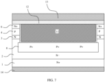
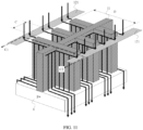
- this application provides a semiconductor device, and the semiconductor device includes an N-type semiconductor substrate, an epitaxial layer, a trench structure, a gate, an interlayer dielectric layer, a source, and a drain.
- the trench structure is disposed at the epitaxial layer.
- the trench structure may specifically include a plurality of first trenches and one second trench. All of the plurality of first trenches extend in a first direction parallel to a plane on which the semiconductor substrate is located, and are arranged at intervals in a second direction parallel to the plane on which the semiconductor substrate is located.
- the second trench extends in the second direction, and the second trench and each of the plurality of first trenches are disposed in a cross manner and communicate with each other.
- a main function of the second trench is to connect the first trenches.
- the tightly arranged trench structure may be formed by disposing the first trench and the second trench at the epitaxial layer.
- the gate is filled and disposed in the trench structure, and is spaced apart by a gate dielectric layer. Parts that are of the gate and that are disposed in the plurality of first trenches extend in the first direction, and parts that are of the gate and that are disposed in the second trench extend in the second direction, and are configured to connect the parts that are of the gate and that extend in the first direction.
- the epitaxial layer may include a first N-type semiconductor region, a second N-type semiconductor region, a first P-type semiconductor region, and a source region that are sequentially disposed on the semiconductor substrate.
- the trench structure may extend to the first N-type semiconductor region.
- the first direction, the second direction, and the third direction are set in a cross manner.
- the first direction, the second direction, and the third direction are set to be perpendicular to each other.
- Existence of the trench structure enables the gate to be built inside the epitaxial layer of a material.
- the gate and the first P-type semiconductor region form a trench gate structure of a SiC MOSFET device by using the gate dielectric layer, so that the semiconductor device provided in this embodiment of this application is a SiC MOSFET of the trench gate structure.
- the interlayer dielectric layer is disposed on the gate and covers the gate.
- the source is disposed at the interlayer dielectric layer. In other words, the source covers the entire interlayer dielectric layer.
- the drain is disposed on a side that is of the semiconductor substrate and that is away from the epitaxial layer. In other words, the drain covers a side that is of the semiconductor substrate and that is not disposed with an epitaxial layer.
- a contact hole extending in the second direction may be disposed at the interlayer dielectric layer. To avoid contact between the source and the gate, a projection of the contact hole in the third direction may not overlap the gate, and the contact hole does not overlap the gate. In addition, the contact hole may expose a partial region of the epitaxial layer.
- the contact hole may expose a partial region of the source region, so that the source is in contact with the source region through the contact hole.
- a signal may be transmitted between the source and the drain.
- Parts of two side walls that are of each first trench in the trench structure and that are disposed opposite to each other in the second direction are channels.
- an extension direction of the contact hole disposed at the interlayer dielectric layer is the second direction
- an extension direction of each first trench in the trench structure is the first direction
- the extension direction of the contact hole is perpendicular to the extension direction of each first trench.
- the contact hole is disposed in a direction perpendicular to a first channel. Therefore, in comparison with a manner, in a conventional technology, in which the trench structure is disposed in parallel to the contact hole, according to the semiconductor device provided in this embodiment of this application, a limitation imposed by the contact hole on a trench spacing between adjacent first trenches in the second direction is reduced, so that the trench structure can be manufactured more tightly. In other words, the gate is also tighter.
- an array density of the trench structure of the semiconductor device provided in this embodiment of this application may be far higher than an array density of a trench structure of a device structure in a conventional technology. Therefore, a channel density of the SiC MOSFET is increased, total on-resistance of the device is clearly reduced, device performance is improved, and a device loss is reduced.
- the semiconductor substrate may be a SiC single crystal substrate doped with a pentavalent element.
- a SiC material that is generated through epitaxial growth and that is doped with a corresponding impurity may be used for the epitaxial layer.
- the first N-type semiconductor region may be a partial region of the epitaxial layer formed through epitaxial growth, and the second N-type semiconductor region and the source region may be formed by doping the epitaxial layer by using an ion implantation process.
- the N-type semiconductor region is mainly doped with an N-type impurity, for example, nitrogen (N), phosphorus (P), or arsenic (As).
- a doping concentration of the semiconductor substrate is usually greater than a doping concentration of the second N-type semiconductor region.
- the doping concentration of the second N-type semiconductor region is usually greater than a doping concentration of the first N-type semiconductor region.
- a doping concentration of the source region is usually greater than the doping concentration of the second N-type semiconductor region.
- the first P-type semiconductor region may be formed by doping the epitaxial layer by using the ion implantation process.
- the P-type semiconductor region is mainly doped with a P-type impurity, for example, boron (B), aluminum (Al), or gallium (Ga).
- a material of a gate 11 is not limited in this application.
- the material of the gate may be a polycrystalline silicon material, or may be another material having a good conductive property, for example, metal (for example, W, Al, Ti, Cu, Mo, or Pt).
- a material for forming the interlayer dielectric layer is not limited in this application.
- the material for forming the interlayer dielectric layer may be a dielectric material.
- the dielectric material includes but is not limited to silicon dioxide (SiO 2 ), silicon nitride (SiNO), silicon carbon oxide (SiCO), silicon nitride (SiNx), and the like.
- a material for forming the source and the drain is not limited in this application.
- the material for forming the source and the drain may be a metal material.
- the metal material may include W, Al, Ti, Cu, Mo, Pt, or the like.
- a trench structure may be disposed between two adjacent contact holes, so that signals can evenly flow.
- structural parameters of the trench structures may be the same, to ensure that the trench structures are evenly distributed.
- quantities of first trenches may be the same
- trench spacings between the first trenches may be the same
- trench lengths of the first trenches may be the same
- lengths of the second trenches may be the same.
- the quantity of first trenches in the trench structure may be determined based on an actual application requirement. This is not limited in this application.
- quantities of first trenches in some trench structures may be the same, and quantities of first trenches in the other trench structures may be different.
- quantities of first trenches in different trench structures may be different.
- the quantity of first trenches in the trench structure may be determined based on an actual application requirement. This is not limited in this application.
- two first trenches that are located at edges of the trench structure may be respectively defined as a first edge trench and a second edge trench
- the contact hole extends, in the second direction, from a side that is of the first edge trench and that is away from the second edge trench to a side that is of the second edge trench and that is away from the first edge trench.
- the contact hole is a continuous opening, and first trenches in different trench structures do not communicate with each other.
- the semiconductor device provided in this embodiment of this application is a SiC MOSFET device of the trench gate structure.
- the gate dielectric layer at a bottom and a corner of the trench structure of the SiC MOSFET device bears extremely high electric field strength when the device works, is a weak point for electric field breakdown, and easily causes a reliability failure when the device works for a long period. Therefore, how to effectively shield the gate dielectric layer from a high electric field stress becomes a key to a high robustness/reliability design of the device.
- a second P-type semiconductor region may be further disposed at the epitaxial layer.
- the second P-type semiconductor region is disposed below the trench structure, and the second P-type semiconductor region may be connected to the source.
- the second P-type semiconductor region may be disposed in direct contact with the bottom of the trench structure.
- the source of the SiC MOSFET may be grounded, and the drain of the SiC MOSFET may be connected to another component.
- the voltage of the source of the SiC MOSFET is a ground voltage (0 V). Because the second P-type semiconductor region is connected to the source, the voltage of the second P-type semiconductor region is also a ground voltage, so that the electric field of the gate dielectric layer at the bottom of the trench structure can be effectively shielded, and working robustness of the device is improved.
- the source of the SiC MOSFET may alternatively be connected to another component, and the drain of the SiC MOSFET is also connected to another component.
- the voltage of the source of the SiC MOSFET is a voltage of a signal input by the another component. Because the second P-type semiconductor region is connected to the source, the voltage of the second P-type semiconductor region is also the voltage of the input signal, so that the electric field of the gate dielectric layer at the bottom of the trench structure can be effectively shielded, and working robustness of the device is improved.
- a thickness of the second P-type semiconductor region in the third direction is not limited in this application.
- a thickness range of the second P-type semiconductor region in the third direction may be less than 1 ⁇ m.
- the thickness range of the second P-type semiconductor region in the third direction may be 0.3 ⁇ m to 0.8 ⁇ m.
- the epitaxial layer may further include a third P-type semiconductor region and a fourth P-type semiconductor region.
- the third P-type semiconductor region is disposed on at least one side wall of the trench structure, and the fourth P-type semiconductor region and the source region are disposed at a same layer.
- the third P-type semiconductor region is in contact with the second P-type semiconductor region.
- the fourth P-type semiconductor region and the third P-type semiconductor region are disposed in a one-to-one correspondence and are in contact with each other.
- the voltage may be input to the second P-type semiconductor region sequentially through the fourth P-type semiconductor region and the third P-type semiconductor region, so that the electric field of the gate dielectric layer at the bottom of the trench structure can be effectively shielded, and working robustness of the device is improved.
- the first P-type semiconductor region, the second P-type semiconductor region, the third P-type semiconductor region, and the fourth P-type semiconductor region may be formed by doping the epitaxial layer by using the ion implantation process.
- the P-type semiconductor region is mainly doped with a P-type impurity, for example, boron (B), aluminum (Al), or gallium (Ga).
- doping concentrations of the second P-type semiconductor region, the third P-type semiconductor region, and the fourth P-type semiconductor region are greater than a doping concentration of the first P-type semiconductor region.
- the doping concentrations of the second P-type semiconductor region, the third P-type semiconductor region, and the fourth P-type semiconductor region may be the same or similar.
- at least two of the doping concentrations of the second P-type semiconductor region, the third P-type semiconductor region, and the fourth P-type semiconductor region may alternatively be different.
- the doping concentrations of the second P-type semiconductor region, the third P-type semiconductor region, and the fourth P-type semiconductor region may be determined based on a requirement of an actual application environment. This is not limited herein.
- each of the plurality of first trenches may have a first side wall and a second side wall that are disposed opposite to each other, and the third P-type semiconductor regions may be disposed on a first side wall and a second side wall of at least one of the plurality of first trenches.
- the first side wall and the second side wall of at least one first trench each are disposed with the third P-type semiconductor region.
- each of the third P-type semiconductor regions is in contact with the second P-type semiconductor region, so that each of the third P-type semiconductor regions is connected to the second P-type semiconductor region to perform signal transmission, and a voltage of each of the third P-type semiconductor regions is the same as the voltage of the second P-type semiconductor region.
- the fourth P-type semiconductor region is in a one-to-one correspondence with and is disposed in contact with the third P-type semiconductor region, and the fourth P-type semiconductor region is in contact with a corresponding source through the contact hole.
- One fourth P-type semiconductor region is disposed in correspondence with the third P-type semiconductor region disposed on the first side wall, and the fourth P-type semiconductor region is disposed on a side that is of the third P-type semiconductor region and that is away from the first side wall of the first trench.
- one fourth P-type semiconductor region is disposed in correspondence with the third P-type semiconductor region disposed on the second side wall, and the fourth P-type semiconductor region is disposed on a side that is of the third P-type semiconductor region and that is away from the second side wall of the first trench.
- the source is connected to the second P-type semiconductor region sequentially through the fourth P-type semiconductor region and the third P-type semiconductor region that are disposed in correspondence with each other, so that the voltage loaded on the source is input to the second P-type semiconductor region sequentially through the fourth P-type semiconductor region and the third P-type semiconductor region, the second P-type semiconductor region has the voltage, the electric field of the gate dielectric layer at the bottom of the trench structure can be effectively shielded, and working robustness of the device is improved.
- a plurality of third P-type semiconductor regions may be disposed.
- the first side wall of each first trench is disposed with one of the plurality of third P-type semiconductor regions
- the second side wall of each first trench is disposed with one of the plurality of third P-type semiconductor regions.
- the first side wall and the second side wall of each first trench each are disposed with the third P-type semiconductor region.
- each of the third P-type semiconductor regions is in contact with the second P-type semiconductor region, so that each of the third P-type semiconductor regions is connected to the second P-type semiconductor region to perform signal transmission, and the voltage of each of the third P-type semiconductor regions is the same as the voltage of the second P-type semiconductor region.
- a plurality of fourth P-type semiconductor regions may be disposed, and the plurality of fourth P-type semiconductor regions are disposed in a one-to-one correspondence and in contact with the plurality of third P-type semiconductor regions.
- One of the plurality of fourth P-type semiconductor regions is disposed in correspondence with the third P-type semiconductor region disposed on the first side wall, and the fourth P-type semiconductor region is disposed on the side that is of the third P-type semiconductor region and that is away from the first side wall of the first trench.
- one of the plurality of fourth P-type semiconductor regions is disposed in correspondence with the third P-type semiconductor region disposed on the second side wall, and the fourth P-type semiconductor region is disposed on the side that is of the third P-type semiconductor region and that is away from the second side wall of the first trench.
- the source is connected to the second P-type semiconductor region sequentially through the fourth P-type semiconductor region and the third P-type semiconductor region that are disposed in correspondence with each other, so that the voltage loaded on the source is input to the second P-type semiconductor region sequentially through the fourth P-type semiconductor region and the third P-type semiconductor region, the second P-type semiconductor region has the voltage, the electric field of the gate dielectric layer at the bottom of the trench structure can be effectively shielded, and working robustness of the device is improved.
- a plurality of source regions may also be disposed.
- a plurality of source regions and a plurality of fourth P-type semiconductor regions that are located at a same end of the trench structure are alternately disposed.
- a plurality of source regions and a plurality of fourth P-type semiconductor regions that are located on first side walls of a plurality of first trenches in a same trench structure are alternately disposed.
- a plurality of source regions and a plurality of fourth P-type semiconductor regions that are located on second side walls of a plurality of first trenches in a same trench structure are alternately disposed.
- a width of the fourth P-type semiconductor region in the second direction is not limited in this application.
- the width of the fourth P-type semiconductor region in the second direction may be the same as or similar to a width of the first trench.
- a width of the source region in the second direction is the same as or similar to the trench spacing between two adjacent first trenches.
- the width of the fourth P-type semiconductor region in the second direction may alternatively be different from the width of the first trench. This is not limited herein.
- a projection of the second P-type semiconductor region in the third direction may cover the trench structure and the third P-type semiconductor region.
- an orthographic projection of the second P-type semiconductor region on the semiconductor substrate not only covers an orthographic projection of the trench structure on the semiconductor substrate, but also covers orthographic projections of all the third P-type semiconductor regions on the semiconductor substrate.
- the second P-type semiconductor region may be a planar region extending in the second direction.
- a shape of the second P-type semiconductor region is not limited in this application.
- the shape of the second P-type semiconductor region may be set to a rectangle.
- the projection of the second P-type semiconductor region in the third direction may further cover a gap between two adjacent first trenches.
- the projection of the second P-type semiconductor region in the third direction may further cover a gap between two adjacent first trenches in the second direction.
- the orthographic projection of the second P-type semiconductor region on the semiconductor substrate further covers an orthographic projection, on the semiconductor substrate, of the gap between two adjacent first trenches in the second direction.
- one second P-type semiconductor region is disposed in correspondence with one trench structure.
- one trench structure is disposed, one second P-type semiconductor region that is a planar region is correspondingly disposed. If two trench structures are disposed, two second P-type semiconductor regions that are planar regions are correspondingly disposed. In addition, there is a gap between the two second P-type semiconductor regions. If a plurality of trench structures are disposed, a plurality of second P-type semiconductor regions that are planar regions are correspondingly disposed. In addition, there is a gap between every two adjacent second P-type semiconductor regions.
- the trench spacing in the second direction, there is a trench spacing between two adjacent first trenches.
- a specific value of the trench spacing is not limited in this application.
- the trench spacing may be less than 1 ⁇ m.
- a range of the trench spacing is 50 nm to 0.5 ⁇ m.
- the semiconductor device provided in this application forms a fin field effect transistor (Fin Field-Effect Transistor, Fin FET) effect, so that channel carrier mobility can be significantly improved, and the total on-resistance of the device can be further reduced.
- Fin FET Fin Field-Effect Transistor
- the first trench has a trench length.
- the trench length is not limited in this application.
- the trench length may be greater than 5 ⁇ m.
- the first trench has a trench width.
- the trench width is not limited in this application.
- the trench width may be less than 1 ⁇ m.
- the contact hole has a contact width, so that the trench spacing is not greater than the contact width.
- the trench spacing may alternatively be greater than the contact width.
- the trench spacing and the contact width may be determined based on an actual application environment requirement. This is not limited herein.
- the first P-type semiconductor regions on two side walls that are of the first trench in the trench structure and that are in the second direction form channel regions of the SiC MOSFET. Therefore, the trench width is increased or the trench spacing is reduced, so that a density of a conductive channel of the SiC MOSFET device can be increased, and the total on-resistance of the SiC MOSFET device can be reduced.
- the semiconductor device may include an N-type semiconductor substrate, an epitaxial layer, a trench structure, a gate, an interlayer dielectric layer, a source, and a drain.
- the epitaxial layer may include a first N-type semiconductor region, a second N-type semiconductor region, a first P-type semiconductor region, a source region, a second P-type semiconductor region, a third P-type semiconductor region, and a fourth P-type semiconductor region.
- the spacing region there is a spacing region between the second P-type semiconductor region and a bottom of the trench structure.
- the second P-type semiconductor region at the bottom of the trench structure is not directly in contact with the bottom of the trench structure, but is connected to the bottom of the trench structure through the spacing region.
- the spacing region may be an N-type semiconductor region, and a doping concentration of the spacing region is the same as or similar to a doping concentration of the first N-type semiconductor region.
- the spacing region may be a part of the first N-type semiconductor region.
- the spacing region may be a flow path of a conduction current of a SiC MOSFET device, so that an area of a through-current region of the SiC MOSFET device can be increased, and total on-resistance of the SiC MOSFET device can be further reduced.
- the semiconductor device may specifically include an N-type semiconductor substrate, an epitaxial layer, a trench structure, a gate, an interlayer dielectric layer, a source, and a drain.
- the epitaxial layer may include a first N-type semiconductor region, a second N-type semiconductor region, a first P-type semiconductor region, a source region, a second P-type semiconductor region, third P-type semiconductor regions, and fourth P-type semiconductor regions.
- a plurality of third P-type semiconductor regions are disposed.
- a first side wall of each first trench is disposed with one of the plurality of third P-type semiconductor regions, and a second side wall of each first trench is not disposed with a third P-type semiconductor region.
- only the first side wall of each first trench is disposed with the third P-type semiconductor region.
- each of the third P-type semiconductor regions is in contact with the second P-type semiconductor region, so that each of the third P-type semiconductor regions is connected to the second P-type semiconductor region to perform signal transmission, and a voltage of each of the third P-type semiconductor regions is the same as a voltage of the second P-type semiconductor region.
- a plurality of fourth P-type semiconductor regions are also disposed, and the plurality of fourth P-type semiconductor regions are disposed in a one-to-one correspondence and in contact with the plurality of third P-type semiconductor regions.
- One of the plurality of fourth P-type semiconductor regions is disposed in correspondence with the third P-type semiconductor region disposed on the first side wall, and the fourth P-type semiconductor region is disposed on a side that is of the third P-type semiconductor region and that is away from the first side wall of the first trench.
- the source is connected to the second P-type semiconductor region sequentially through the fourth P-type semiconductor region and the third P-type semiconductor region that are disposed in correspondence with each other, so that a voltage loaded on the source is input to the second P-type semiconductor region sequentially through the fourth P-type semiconductor region and the third P-type semiconductor region, the second P-type semiconductor region has a voltage, an electric field of a gate dielectric layer at a bottom of the trench structure can be effectively shielded, and working robustness of the device is improved.
- the epitaxial layer may further include a fifth P-type semiconductor region.
- the fifth P-type semiconductor region and the source region are disposed at a same layer.
- the fifth P-type semiconductor region is disposed on a side that is of the second side wall of the first trench and that is away from the first side wall, and the fifth P-type semiconductor region is in contact with the source through a contact hole.
- a plurality of fifth P-type semiconductor regions may be disposed, and the plurality of fifth P-type semiconductor regions are disposed in a one-to-one correspondence with the second side walls of all the first trenches.
- a plurality of source regions and the plurality of fifth P-type semiconductor regions that are located on second side walls of the first trenches are alternately disposed.
- the fifth P-type semiconductor region may be formed by doping the epitaxial layer by using an ion implantation process.
- the fifth P-type semiconductor region is mainly doped with a P-type impurity, for example, boron (B), aluminum (Al), or gallium (Ga).
- a doping concentration of the fifth P-type semiconductor region may be the same as or similar to a doping concentration of the fourth P-type semiconductor region.
- the first side wall of the first trench is disposed with the third P-type semiconductor region, and no channel is formed.
- the semiconductor device may specifically include an N-type semiconductor substrate, an epitaxial layer, a trench structure, a gate, an interlayer dielectric layer, a source, and a drain.
- the epitaxial layer may include a first N-type semiconductor region, a second N-type semiconductor region, a first P-type semiconductor region, a source region, a second P-type semiconductor region, third P-type semiconductor regions, and fourth P-type semiconductor regions.
- a plurality of third P-type semiconductor regions are disposed.
- a first side wall of each first trench is disposed with one of the plurality of third P-type semiconductor regions, and a second side wall of each first trench is not disposed with a third P-type semiconductor region.
- only the first side wall of each first trench is disposed with the third P-type semiconductor region.
- each of the third P-type semiconductor regions is in contact with the second P-type semiconductor region, so that each of the third P-type semiconductor regions is connected to the second P-type semiconductor region to perform signal transmission, and a voltage of each of the third P-type semiconductor regions is the same as a voltage of the second P-type semiconductor region.
- a plurality of fourth P-type semiconductor regions are also disposed, and the plurality of fourth P-type semiconductor regions are disposed in a one-to-one correspondence and in contact with the plurality of third P-type semiconductor regions.
- One of the plurality of fourth P-type semiconductor regions is disposed in correspondence with the third P-type semiconductor region disposed on the first side wall, and the fourth P-type semiconductor region is disposed on a side that is of the third P-type semiconductor region and that is away from the first side wall of the first trench.
- the source is connected to the second P-type semiconductor region sequentially through the fourth P-type semiconductor region and the third P-type semiconductor region that are disposed in correspondence with each other, so that a voltage loaded on the source is input to the second P-type semiconductor region sequentially through the fourth P-type semiconductor region and the third P-type semiconductor region, the second P-type semiconductor region has a voltage, an electric field of a gate dielectric layer at a bottom of the trench structure can be effectively shielded, and working robustness of the device is improved.
- only the first side wall of the first trench is disposed with the fourth P-type semiconductor region, and the second side wall of the first trench is disposed with only the source region.
- positions of the first side wall and the second side wall of the first trench may also be interchanged.
- the second side wall of the first trench may be disposed with one of the plurality of third P-type semiconductor regions, and the first side wall of each first trench is not disposed with a third P-type semiconductor region.
- the semiconductor device may specifically include an N-type semiconductor substrate, an epitaxial layer, a trench structure, a gate, an interlayer dielectric layer, a source, and a drain.
- the epitaxial layer may include a first N-type semiconductor region, a second N-type semiconductor region, a first P-type semiconductor region, a source region, a second P-type semiconductor region, third P-type semiconductor regions, and fourth P-type semiconductor regions.
- At least one end part of a second trench may extend out of a first trench located at an edge in the plurality of first trenches.
- the second trench may have a third side wall and a fourth side wall that are disposed opposite to each other, and the third P-type semiconductor region may be disposed on the third side wall and/or the fourth side wall of the second trench.
- both end parts of the second trench may extend out of the first trench located at the edge in the plurality of first trenches, and the third P-type semiconductor regions may be disposed on the third side wall and the fourth side wall of the second trench.
- the third side wall and the fourth side wall of the second trench each are disposed with the third P-type semiconductor region.
- each of the third P-type semiconductor regions is in contact with the second P-type semiconductor region, so that each of the third P-type semiconductor regions is connected to the second P-type semiconductor region to perform signal transmission, and a voltage of each of the third P-type semiconductor regions is the same as a voltage of the second P-type semiconductor region.
- the fourth P-type semiconductor region is disposed in a one-to-one correspondence and in contact with the third P-type semiconductor region.
- One fourth P-type semiconductor region is disposed in correspondence with the third P-type semiconductor region disposed on the third side wall, and the fourth P-type semiconductor region is disposed on a side that is of the third P-type semiconductor region and that is away from the third side wall of the second trench.
- one fourth P-type semiconductor region is disposed in correspondence with the third P-type semiconductor region disposed on the fourth side wall, and the fourth P-type semiconductor region is disposed on a side that is of the third P-type semiconductor region and that is away from the fourth side wall of the second trench.
- a voltage may be input to the second P-type semiconductor region sequentially through the fourth P-type semiconductor region and the third P-type semiconductor region, so that the second P-type semiconductor region has a voltage, an electric field of a gate dielectric layer at a bottom of the trench structure can be effectively shielded, and working robustness of the device is improved.
- the epitaxial layer may further include a fifth P-type semiconductor region.
- the fifth P-type semiconductor region and the source region are disposed at a same layer.
- the fifth P-type semiconductor region may be disposed on a side that is of a second side wall of the first trench and that is away from a first side wall.
- the fifth P-type semiconductor region may be further disposed on a side that is of the first side wall of the first trench and that is away from the second side wall, and the fifth P-type semiconductor region is in contact with the source through a contact hole.
- a plurality of fifth P-type semiconductor regions may be disposed, and the plurality of fifth P-type semiconductor regions are disposed in a one-to-one correspondence with the first side walls and the second side walls of all the first trenches.
- a plurality of source regions and a plurality of fifth P-type semiconductor regions that are located on first side walls of the first trenches are alternately disposed, and a plurality of source regions and a plurality of fifth P-type semiconductor regions that are located on second side walls of the first trenches are alternately disposed.
- the fifth P-type semiconductor region may be formed by doping the epitaxial layer by using an ion implantation process.
- the fifth P-type semiconductor region is mainly doped with a P-type impurity, for example, boron (B), aluminum (Al), or gallium (Ga).
- a doping concentration of the fifth P-type semiconductor region may be the same as or similar to a doping concentration of the fourth P-type semiconductor region.
- the third side wall and the fourth side wall of the second trench are disposed with the third P-type semiconductor regions, and no channel is formed.
- the semiconductor device may specifically include an N-type semiconductor substrate, an epitaxial layer, a trench structure, a gate, an interlayer dielectric layer, a source, and a drain.
- the epitaxial layer may include a first N-type semiconductor region, a second N-type semiconductor region, a first P-type semiconductor region, a source region, a second P-type semiconductor region, a third P-type semiconductor region, and a fourth P-type semiconductor region.
- the first trenches arranged in a first direction communicate with each other.
- a plurality of first trenches may include a first gate trench and a second gate trench that communicate with each other in the first direction.
- the first gate trench and the second gate trench may be considered to be respectively located in two adjacent trench structures.
- first edge trenches in two adjacent trench structures on the left and right sides are arranged in the first direction, and the two first edge trenches communicate with each other.
- Second edge trenches in two adjacent trench structures on the left and right sides are arranged in the first direction, and the two second edge trenches communicate with each other.
- a first trench in the middle of a left-side trench structure and a first trench in the middle of a right-side trench structure may also communicate with each other.
- a contact hole may include a plurality of contact sub-holes that are disposed at intervals, and at least one first trench that is through is disposed between two adjacent contact sub-holes in a same contact hole.
- a quantity of the contact sub-holes that the contact hole is divided into is not limited in this application. For example, there may be two, three, four, or more contact sub-holes.
- a quantity of first trenches that are through and that are disposed between two adjacent contact sub-holes in a same contact hole is not limited in this application. For example, there may be one, two, three, four, or more first trenches. In this way, design freedom of the contact hole can be improved, and through-current uniformity of a SiC MOSFET device can be improved.
- the semiconductor device may specifically include an N-type semiconductor substrate, an epitaxial layer, a trench structure, a gate, an interlayer dielectric layer, a source, and a drain.
- the epitaxial layer may include a third N-type semiconductor region, a first N-type semiconductor region, a second N-type semiconductor region, a first P-type semiconductor region, a source region, a second P-type semiconductor region, a third P-type semiconductor region, and a fourth P-type semiconductor region.
- This embodiment is a variant of the implementations in the foregoing embodiment. The following describes only differences between this embodiment and the foregoing embodiment, and the same parts are not described herein again.
- the third N-type semiconductor region may be disposed between the first N-type semiconductor region and the semiconductor substrate. Because the third N-type semiconductor region is disposed, a thickness of the second P-type semiconductor region at the epitaxial layer in the third direction may be set to be thicker. For example, the thickness of the second P-type semiconductor region in the third direction may be set to be greater than 1 ⁇ m.
- the third N-type semiconductor region may be SiC doped with an N-type impurity.
- the N-type impurity is, for example, nitrogen (N), phosphorus (P), or arsenic (As).
- a doping concentration of the third N-type semiconductor region may be less than a doping concentration of the first N-type semiconductor region.
- an embodiment of this application further provides a manufacturing method for a semiconductor device.
- the manufacturing method may include the following steps: epitaxially growing an epitaxial layer on an N-type semiconductor substrate; etching at the epitaxial layer to form a trench structure, where the trench structure includes a plurality of first trenches and one second trench, all of the plurality of first trenches extend in a first direction parallel to a plane on which the semiconductor substrate is located, and are arranged at intervals in a second direction parallel to the plane on which the semiconductor substrate is located, the second trench extends in the second direction, and the second trench and each of the plurality of first trenches are disposed in a cross manner and communicate with each other; sequentially forming a gate dielectric layer and a gate in the trench structure; forming, on the gate, an interlayer dielectric layer that covers the epitaxial layer; etching the interlayer dielectric layer to form a contact hole extending in the second direction, where the contact hole exposes a partial region of the epitaxial
- the manufacturing method may further include: before the sequentially forming a gate dielectric layer and a gate in the trench structure, forming, by using a tilted ion implantation process on at least one side wall of the trench structure, a third P-type semiconductor region in contact with a second P-type semiconductor region; and forming, at the epitaxial layer by using an ion implantation process, a fourth P-type semiconductor region disposed at a same layer as a source region.
- the epitaxially growing an epitaxial layer on an N-type semiconductor substrate may include the following steps:
- an epitaxial layer that reaches a first specified thickness (that is, a thickness in the third direction) is epitaxially grown on the N-type SiC semiconductor substrate.
- a SiC material doped with an N-type impurity is epitaxially grown on the N-type SiC semiconductor substrate by using an epitaxial growth process, to form the epitaxial layer that reaches the first specified thickness.
- a specific value of the first specified thickness is not limited in this application. In actual application, the specific value of the first specified thickness may be determined based on a requirement of an actual application environment.
- ion implantation is performed at the epitaxial layer by using the ion implantation process, to form a second P-type semiconductor region.
- a P-type impurity is doped, by using the ion implantation process, in the to-be-formed second P-type semiconductor region at the epitaxial layer, to form the second P-type semiconductor region that is a planar region.
- a thickness of the second P-type semiconductor region (that is, a thickness in the third direction) is not limited in this application. In actual application, a specific value of the thickness of the second P-type semiconductor region may be determined based on a requirement of an actual application environment.
- epitaxial growth is continued at the epitaxial layer at which the second P-type semiconductor region is formed, until an epitaxial layer that reaches a second specified thickness is formed.
- the SiC material doped with the N-type impurity continues to be epitaxially grown, by using the epitaxial growth process, at the epitaxial layer at which the second P-type semiconductor region is formed, to form the first epitaxial layer that reaches the second specified thickness.
- the manufacturing method may further include: performing ion implantation in a partial region of the epitaxial layer by using the ion implantation process, to sequentially form a second N-type semiconductor region, a first P-type semiconductor region, and the source region, where a region that is of the epitaxial layer and in which ion implantation is not performed forms a first N-type semiconductor region.
- performing ion implantation in a partial region of the epitaxial layer by using the ion implantation process to sequentially form a second N-type semiconductor region, a first P-type semiconductor region, and the source region, where a region that is of the epitaxial layer and in which ion implantation is not performed forms a first N-type semiconductor region.
- the region that is of the epitaxial layer and in which ion implantation is not performed forms the first N-type semiconductor region.
- the performing ion implantation in a partial region of the epitaxial layer by using the ion implantation process, to sequentially form a second N-type semiconductor region, a first P-type semiconductor region, and the source region, where a region that is of the first epitaxial layer and in which ion implantation is not performed forms a first N-type semiconductor region may include the following steps:
- the N-type impurity is doped on a surface of the epitaxial layer by using the ion implantation process, to form the second N-type semiconductor region.
- the P-type impurity is doped on the surface of the epitaxial layer by using the ion implantation process, to form the first P-type semiconductor region.
- the N-type impurity is doped on the surface of the epitaxial layer by using the ion implantation process, to form the source region, and the P-type impurity doped on a surface of the epitaxial layer that is on a first side wall and a second side wall of the first trench, to form the fourth P-type semiconductor region disposed at a same layer as the source region.
- the partial region of the epitaxial layer forms the second N-type semiconductor region, the first P-type semiconductor region, the source region, and the fourth P-type semiconductor region, and the region that is of the epitaxial layer and in which ion implantation is not performed by using the ion implantation process forms the first N-type semiconductor region.
- etching the epitaxial layer until the first N-type semiconductor region is etched may include the following steps:
- a trench mask is formed at the epitaxial layer (where the trench mask may be a mask formed by using photoresist or a hard mask plate). A region that is of the epitaxial layer and that does not need to form the trench structure is covered with the trench mask, and a region that is of the epitaxial layer and that needs to form the trench structure is exposed.
- an appropriate etching process is selected from a plasma etching process, an ion sputtering etching process, a reactive ion etching process, and the like, to etch region that is of the epitaxial layer and that is not covered with the trench mask, and stop etching when the first N-type semiconductor region is etched and the second P-type semiconductor region is exposed, to form, at the epitaxial layer, the trench structure including the plurality of first trenches and the second trench.
- the third P-type semiconductor region in contact with the second P-type semiconductor region may include the following steps:
- the P-type impurity is doped on surfaces of the first side wall and the second side wall of each first trench by using the tilted ion implantation process, to separately form the third P-type semiconductor region in contact with the second P-type semiconductor region.
- forming the gate dielectric layer in the trench structure may include the following steps: Oxidation processing is performed on a surface of the trench structure by using an oxidation process, so that the gate dielectric layer is formed on the surface of the trench structure.
- forming the gate in the trench structure in which the gate dielectric layer is formed may include the following steps:
- a polycrystalline silicon material is deposited, by using a deposition process, at the entire epitaxial layer at which the trench structure is formed, so that the polycrystalline silicon material is filled in the trench structure, and the entire epitaxial layer is covered with a polycrystalline silicon material film layer after the trench structure is filled with the polycrystalline silicon material.
- an appropriate etching process is selected from a plasma etching process, an ion sputtering etching process, a reactive ion etching process, and the like, to etch a polycrystalline silicon material region that is not covered with the trench mask, and stop etching when the source region and the fourth P-type semiconductor region are exposed, to form the gate.
- forming, on the gate may include the following steps: The interlayer dielectric layer is deposited at the entire epitaxial layer by using the deposition process, and the interlayer dielectric layer covers the entire epitaxial layer.
- the etching the interlayer dielectric layer to form a contact hole extending in the second direction may include the following steps:
- a mask of the contact hole is formed at the epitaxial layer (where the mask of the contact hole may be a mask formed by using photoresist or a hard mask plate). A region that does not need to form the contact hole is covered with the mask of the contact hole, and a region that needs to form the contact hole is exposed.
- an appropriate etching process is selected from a plasma etching process, an ion sputtering etching process, a reactive ion etching process, and the like, to etch the region that is of the interlayer dielectric layer and that is not covered with the mask of the contact hole, expose a partial region of the source region, for example, parts of the source region that are in the first direction and that are located on two sides of the gate, and expose parts of the fourth P-type semiconductor region that are located on the two sides of the gate.
- forming the source at the interlayer dielectric layer, where the source is in contact with the source region through the contact hole, and forming the drain on the side that is of the semiconductor substrate and that is away from the epitaxial layer may include the following steps:
- a metal material is deposited at the interlayer dielectric layer by using the deposition process, to form the source.
- the contact hole is filled with the metal material, so that the source is in contact with the source region by using the metal material filled in the contact hole.
- the metal material may be deposited, by using the deposition process, on the side that is of the semiconductor substrate and that is away from the epitaxial layer, to form the drain.
- the metal material may be deposited, by using the deposition process, on the side that is of the semiconductor substrate and that is away from the epitaxial layer, to form the drain.
- a material of the source and the drain is not limited in this application.
- the material for forming the source and the drain may be a metal material.
- the metal material may include W, Al, Ti, Cu, Mo, or Pt.
- an embodiment of this application further provides a power conversion circuit.
- the power conversion circuit may be an alternating current-direct current conversion circuit and/or a direct current-direct current conversion circuit.
- the power conversion circuit may include a circuit board and one or more semiconductor devices, and the semiconductor device is connected to the circuit board.
- the semiconductor device may be the semiconductor device according to the first aspect or various possible designs of the first aspect, or the semiconductor device manufactured according to the second aspect or various possible designs of the second aspect. Because performance of the foregoing semiconductor device is good, performance of a power conversion circuit including the foregoing semiconductor device is also good.
- a problem-resolving principle of the power conversion circuit is similar to a problem-resolving principle of the foregoing semiconductor device. Therefore, for technical effects of the power conversion circuit, refer to technical effects of the foregoing semiconductor device. Repeated content is not described again.
- an embodiment of this application further provides a vehicle, and the vehicle may include a power conversion circuit.
- the power conversion circuit may be the power conversion circuit according to the third aspect or various possible designs of the third aspect. Because performance of the foregoing power conversion circuit is good, circuit performance of a vehicle including the foregoing power conversion circuit is also good.
- a problem-resolving principle of the vehicle is similar to a problem-resolving principle of the foregoing power conversion circuit. Therefore, for technical effects of the vehicle, refer to technical effects of the foregoing power conversion circuit. Repeated content is not described again.
- 010 electric vehicle; 012: storage battery; 0100: electronic device; 0110: power conversion circuit; 0120: load module; 0200: power supply; 0111: DC-DC converter; 1: semiconductor substrate; 100: epitaxial layer; 2: first N-type semiconductor region; 3: second N-type semiconductor region; 4: first P-type semiconductor region; 5: fourth P-type semiconductor region; 6: source region; 7: trench structure; 8: second P-type semiconductor region; 9: third P-type semiconductor region; 10: gate dielectric layer; 11: gate; 12: interlayer dielectric layer; 13: source; 14: drain; 15: fifth P-type semiconductor region; 16: third N-type semiconductor region; 202: spacing region; 71: first trench; 72: second trench; 121: contact hole; x: first direction; y: second direction; z: third direction; C: trench spacing; D: trench length; E: trench width; F: contact width; S1: first side wall; S2: second side wall; S3: third side wall; S4: fourth side wall;
- connection in embodiments of this application means an electrical connection, and a connection of two electrical components may be a direct or indirect connection between two electrical components.
- a connection between A and B may be either a direct connection between A and B, or an indirect connection between A and B through one or more other electrical components.
- the connection between A and B may be that A and C are directly connected, C and B are directly connected, and A and B are connected through C.
- example implementations may be implemented in a plurality of forms and should not be construed as being limited to implementations described herein, but instead, these implementations are provided to make this application thorough and complete, and to fully convey the concept of the example implementations to a person skilled in the art.
- a same reference sign denotes a same or similar structure in the drawings, and therefore repeated descriptions thereof are omitted.
- the words expressing a position and a direction described in this application are all described by using the accompanying drawings as an example, but changes may also be made as required, and all the changes fall within the protection scope of this application.
- the accompanying drawings in this application are merely used to illustrate relative positional relationships and do not represent a real scale.
- the semiconductor device provided in embodiments of this application may be used in a vehicle (for example, an electric vehicle), for example, may be used in an on-board micro controller unit (micro controller unit, MCU) or an on-board battery charger (on-board battery charger, OBC). It should be noted that the semiconductor device provided in embodiments of this application is intended to include but is not limited to being used in these devices and any other device of a proper type. The following provides descriptions by using an example in which the vehicle is an electric vehicle.
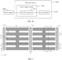
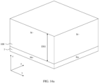
- FIG. 2a is a schematic diagram of a structure of an electric vehicle according to an embodiment of this application.
- the electric vehicle 010 may include a power conversion circuit 0110 and a storage battery 012.
- the power conversion circuit 0110 may include an alternating current (Alternating Current, AC)-direct current (Direct Current, DC) conversion circuit and a DC-DC conversion circuit, and the power conversion circuit 0110 may also be referred to as an inverter.
- the electric vehicle 010 when the electric vehicle is charged, the electric vehicle 010 may be connected to a three-phase power grid, and receive a three-phase alternating current supplied by the three-phase power grid.
- a power switching transistor of the AC-DC conversion circuit of the power conversion circuit 0110 is controlled to work, so that the AC-DC conversion circuit can convert the three-phase alternating current into the direct current.
- a power switching transistor of the DC-DC conversion circuit of the power conversion circuit 0110 is controlled to work, so that the DC-DC conversion circuit can perform voltage regulation on the direct current output by the AC-DC conversion circuit, to supply a voltage-adapted direct current to the storage battery 012.
- the storage battery 012 can store the direct current, and a function of charging can be implemented.
- the power conversion circuit 0110 may alternatively be the DC-DC conversion circuit, and the electric vehicle 010 may further include a load 013.
- the load 013 may be a vehicle-mounted device, a power system, or the like of the electric vehicle 010.
- the power switching transistor of the DC-DC conversion circuit of the power conversion circuit 0110 is controlled to work, so that the power conversion circuit 0110 can perform voltage regulation on a direct current output by the storage battery and then output the direct current to the load 013, to supply the voltage-adapted direct current to the load 013.
- a semiconductor device provided in embodiments of this application is a MOSFET of a trench gate structure.
- a density of a conduction channel can be increased, and resistance of a JFET region is not increased, so that total on-resistance is reduced, device performance is improved, and a device loss is reduced.
- the semiconductor device provided in embodiments of this application may be used in a power conversion circuit 0110 of a vehicle as a power switching transistor of an AC-DC converter and/or a DC-DC converter.
- the semiconductor device provided in embodiments of this application may also be widely used in various electronic devices, for example, may be used in an electronic device having a logic device or a storage device.
- the electronic device may be a smartphone, a smart television, a notebook computer, a personal digital assistant (personal digital assistant, PDA), a wearable device (for example, a smartwatch, smart glasses, or a smart band) having a wireless communication function, or the like.
- PDA personal digital assistant
- a wearable device for example, a smartwatch, smart glasses, or a smart band having a wireless communication function, or the like.
- the semiconductor device provided in embodiments of this application is intended to include but is not limited to being used in these electronic devices and any other electronic device of a proper type.
- FIG. 2b is a schematic diagram of a structure of an electronic device according to an embodiment of this application.
- the electronic device 0100 provided in this embodiment of this application includes a power conversion circuit 0110 and a load module 0120.
- the power conversion circuit 0110 is electrically connected to the load module 0120.
- the electronic device 0100 may be any electric device.
- the electronic device 0100 may be a smartphone, a smart television, a notebook computer, a personal digital assistant (personal digital assistant, PDA), a wearable device (for example, a smartwatch, smart glasses, or a smart band) having a wireless communication function, an on-board micro controller unit (micro controller unit, MCU), or an on-board battery charger (on-board battery charger, OBC).
- a specific type of the electronic device is not limited in this application.
- the power conversion circuit 0110 may be a direct current (direct current, DC)-direct current power conversion circuit, and is configured to output a direct current after performing boost or buck conversion processing on the direct current, to supply power to the load module 0120.
- the power conversion circuit 0110 may convert a direct current (for example, 48 V) output by a power supply 0200 into a direct current used for all types of load modules 0120, and output the direct current to the load module 0120, so that the load module 0120 works.
- the power supply 0200 and the load module 0120 are not limited in this application.
- the power supply 0200 may be any device or component that can output a direct current.
- the power supply 0200 may be a battery (for example, a storage battery).
- the power conversion circuit 0110 may receive a battery voltage supplied by the battery, convert the battery voltage into a working voltage of the load module 0120, and output the working voltage to the load module 0120.
- the load module 0120 may be any function module that uses a direct current.
- the load module 0120 may be a processor, a chip, or the like.
- the power conversion circuit 0110 may include a DC-DC converter 0111.
- a MOSFET in the DC-DC converter 0111 works at a specific switching frequency, so that the DC-DC converter 0111 performs boost or buck conversion processing on a direct current of the power supply 0200, and then outputs the direct current to the load module 0120, to supply a direct current of the working voltage.
- the DC-DC converter may be, for example, a Buck (buck) converter, a Boost (boost) converter, a half-bridge converter, a full-bridge converter, and an inductor-inductor-capacitor (inductor-inductor-capacitor, LLC) resonant converter.
- a semiconductor device provided in embodiments of this application is a MOSFET of a trench gate structure.
- a density of a conduction channel can be increased, and resistance of a JFET region is not increased, so that total on-resistance is reduced, device performance is improved, and a device loss is reduced.
- the semiconductor device provided in embodiments of this application may be used in the DC-DC converter 0111 as a MOSFET in the DC-DC converter 0111. Because device performance of the semiconductor device provided in embodiments of this application is good, when the semiconductor device is used in the MOSFET in the DC-DC converter 0111, performance of the DC-DC converter 0111 can be improved and a drive loss can be reduced, so that performance of the entire electronic device is improved and the drive loss is reduced.
- materials of a semiconductor substrate 1 and an epitaxial layer 100 may be SiC.
- the semiconductor device provided in embodiments of this application is a SiC MOSFET.
- N or P respectively indicates that an electron or a hole is a majority carrier.
- "+" marked beside N or P indicates a higher doping concentration than a doping concentration of a layer or region not marked with "+”, and a larger quantity of "+” indicates a higher doping concentration.
- Ns or Ps that include a same quantity of "+” indicate similar doping concentrations not limited to a same doping concentration.
- N or P indicates a lower doping concentration than a doping concentration of a layer or region not marked with "-”, and a larger quantity of "-" indicates a lower doping concentration.
- Ns or Ps that include a same quantity of "-" indicate similar doping concentrations not limited to a same doping concentration.
- a comparison between doping concentrations of two regions is merely a comparison between concentrations of impurities doped in the two regions.
- a component of an impurity and a material of a substrate doped with the impurity are not limited. In other words, components of the impurities may be the same or may be different. Materials of substrates doped with the impurities may be the same or may be different.
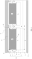
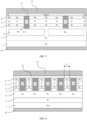
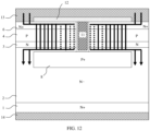
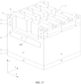
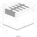
- FIG. 3 shows a schematic diagram of a top-view structure of a semiconductor device according to an embodiment of this application.
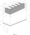
- FIG. 4 shows a schematic diagram of a sectional-view structure in a tangential direction of A1A2 in FIG. 3 .
- FIG. 5 shows a schematic diagram of a sectional-view structure in a tangential direction of A3A4 in FIG. 3 .
- FIG. 6 shows a schematic diagram of a sectional-view structure in a tangential direction of V1V2 in FIG. 3 .
- FIG. 7 shows a schematic diagram of a sectional-view structure in a tangential direction of V3V4 in FIG. 3 .
- FIG. 8 shows a schematic diagram of a partial three-dimensional structure in FIG. 3 .
- FIG. 9 shows a schematic diagram of a three-dimensional structure existing when the semiconductor device shown in FIG. 8 is not provided with an interlayer dielectric layer 12 or a source 13.
- FIG. 10 shows a schematic diagram of a three-dimensional structure of a trench structure in the semiconductor device shown in FIG. 8 .
- the semiconductor device provided in this embodiment of this application may specifically include an N-type semiconductor substrate 1, an epitaxial layer 100, a trench structure 7, a gate 11, an interlayer dielectric layer 12, a source 13, and a drain 14.
- the epitaxial layer 100 includes a first N-type semiconductor region 2, a second N-type semiconductor region 3, a first P-type semiconductor region 4, and a source region 6 that are sequentially disposed on the semiconductor substrate 1.
- the semiconductor substrate 1 may be a SiC single crystal substrate doped with a pentavalent element.
- a SiC material that is generated through epitaxial growth and that is doped with a corresponding impurity may be used for the epitaxial layer 100.
- the first N-type semiconductor region 2 may be a partial region of the epitaxial layer 100 formed through epitaxial growth, and the second N-type semiconductor region 3 and the source region 6 may be formed by doping the epitaxial layer 100 by using an ion implantation process.
- the N-type semiconductor region is mainly doped with an N-type impurity, for example, nitrogen (N), phosphorus (P), or arsenic (As).
- a doping concentration of the semiconductor substrate 1 is usually greater than a doping concentration of the second N-type semiconductor region 3
- a doping concentration of the second N-type semiconductor region 3 is usually greater than a doping concentration of the first N-type semiconductor region 2
- a doping concentration of the source region 6 is usually greater than a doping concentration of the second N-type semiconductor region 3.
- the first P-type semiconductor region 4 may be formed by doping the epitaxial layer 100 by using the ion implantation process.
- the P-type semiconductor region is mainly doped with a P-type impurity, for example, boron (B), aluminum (Al), or gallium (Ga).
- the trench structure 7 is disposed at the epitaxial layer 100, and in a third direction z perpendicular to a plane on which the semiconductor substrate 1 is located, the trench structure 7 extends to the first N-type semiconductor region 2.
- the trench structure 7 may specifically include a plurality of first trenches 71 and one second trench 72. All of the plurality of first trenches 71 extend in a first direction x parallel to the plane on which the semiconductor substrate 1 is located, and are arranged at intervals in a second direction y parallel to the plane on which the semiconductor substrate 1 is located.
- the second trench 72 extends in the second direction y, and the second trench 72 and each of the plurality of first trenches 71 are disposed in a cross manner and communicate with each other.
- a main function of the second trench 72 is to connect the first trenches 71.
- the tightly arranged trench structure 7 may be formed by disposing the first trench 71 and the second trench 72 at the epitaxial layer 100.
- the first direction x, the second direction y, and the third direction z are set in a cross manner.
- the first direction x, the second direction y, and the third direction z are set to be perpendicular to each other.
- the gate 11 is filled and disposed in the trench structure 7, and is spaced apart by a gate dielectric layer 10. Parts that are of the gate 11 and that are disposed in the plurality of first trenches 71 extend in the first direction x, and parts that are of the gate 11 and that are disposed in the second trench 72 extend in the second direction y, and are configured to connect the parts that are of the gate 11 and that extend in the first direction x.
- Existence of the trench structure 7 enables the gate 11 to be built inside the epitaxial layer 100 of the SiC material.
- the gate 11 and the first P-type semiconductor region 4 form a trench gate structure of a SiC MOSFET device by using the gate dielectric layer 10, so that the semiconductor device provided in this embodiment of this application is a SiC MOSFET of the trench gate structure.
- a material of the gate 11 is not limited in this application.
- the material of the gate 11 may be a polycrystalline silicon material, or may be another material having a good conductive property, for example, metal (for example, W, Al, Ti, Cu, Mo, or Pt).
- the interlayer dielectric layer 12 is disposed on the gate 11 and covers the gate 11.
- the source 13 is disposed at the interlayer dielectric layer 12. In other words, the source 13 covers the entire interlayer dielectric layer 12.
- the drain 14 is disposed on a side that is of the semiconductor substrate 1 and that is away from the epitaxial layer 100. In other words, the drain 14 covers a side that is of the semiconductor substrate 1 and that is not disposed with an epitaxial layer 100.
- a contact hole 121 extending in the second direction y may be disposed in the interlayer dielectric layer 12.
- a projection of the contact hole 121 in the third direction z may not overlap the gate 11.
- the contact hole 121 does not overlap the gate 11.
- the contact hole 121 exposes a partial region of the source region 6.
- the contact hole 121 may expose a part, of the source region 6, that is located on two sides of the gate 11 and that is in the first direction x, so that the source 13 can be in contact with the source region 6 through the contact hole 121, and effect of connecting the source 13 to the source region 6 is implemented.
- a signal may be transmitted between the source 13 and the drain 14, where parts of two side walls that are of each first trench 71 in the trench structure 7 and that are disposed opposite to each other in the second direction y are channels.
- a material for forming the interlayer dielectric layer 12 is not limited in this application.
- the material for forming the interlayer dielectric layer 12 may be a dielectric material.
- the dielectric material includes but is not limited to silicon dioxide (SiO 2 ), silicon nitride (SiNO), silicon carbon oxide (SiCO), silicon nitride (SiNx), and the like.
- a material for forming the source 13 and the drain 14 is not limited in this application.
- the material for forming the source 13 and the drain 14 may be a metal material.
- the metal material may include W, Al, Ti, Cu, Mo, Pt, or the like.
- an extension direction of the contact hole 121 disposed in the interlayer dielectric layer 12 is the second direction y
- an extension direction of each first trench 71 in the trench structure 7 is the first direction x
- the extension direction of the contact hole 121 is perpendicular to the extension direction of each first trench 71.
- the contact hole 121 is disposed in a direction perpendicular to a first channel 71.
- an array density of the trench structure of the semiconductor device provided in this embodiment of this application may be far higher than an array density of a trench structure of a device structure in a conventional technology. Therefore, a channel density of the SiC MOSFET is increased, total on-resistance of the device is clearly reduced, device performance is improved, and a device loss is reduced.
- one trench structure 7 may be disposed between two adjacent contact holes 121, so that signals can evenly flow.
- FIG. 3 to FIG. 5 two trench structures 7 and three contact holes 121 are illustrated.
- structural parameters of the trench structures 7 may be the same, to ensure that the trench structures 7 are evenly distributed.
- quantities of first trenches 71 may be the same
- trench spacings between the first trenches 71 may be the same
- trench lengths of the first trenches 71 may be the same
- lengths of the second trenches 72 may be the same.
- the two trench structures 7 each are disposed with five first trenches 71. It should be noted that the quantity of first trenches 71 disposed in the trench structure 7 shown in FIG. 3 is merely for explanation and description, and does not limit a quantity of first trenches 71 in an actually manufactured semiconductor device. In actual application, the quantity of first trenches 71 in the trench structure 7 may be determined based on an actual application requirement. This is not limited in this application.
- quantities of first trenches 71 in some trench structures 7 may be the same, and quantities of first trenches 71 in the other trench structures 7 may be different.
- quantities of first trenches 71 in different trench structures 7 may be different.
- the quantity of first trenches 71 in the trench structure 7 may be determined based on an actual application requirement. This is not limited in this application.
- two first trenches 71 that are located at edges of the trench structure 7 may be respectively defined as a first edge trench and a second edge trench, and the contact hole 121 extends, in the second direction, from a side that is of the first edge trench and that is away from the second edge trench to a side that is of the second edge trench and that is away from the first edge trench.
- the contact hole 121 extends, in the second direction, from a side that is of the first edge trench and that is away from the second edge trench to a side that is of the second edge trench and that is away from the first edge trench.
- first trenches 71 that are located at upper and lower edges of the two trench structures 7 are respectively defined as the first edge trench and the second edge trench
- the contact hole 121 extends, in the second direction y, from the side that is of the first edge trench and that is away from the second edge trench to the side that is of the second edge trench and that is away from the first edge trench.
- the contact hole 121 is a continuous opening, and first trenches 71 in different trench structures 7 do not communicate with each other.
- the semiconductor device provided in this embodiment of this application is a SiC MOSFET device of the trench gate structure.
- the gate dielectric layer 10 at a bottom and a corner of the trench structure 7 of the SiC MOSFET device bears extremely high electric field strength when the device works, is a weak point for electric field breakdown, and easily causes a reliability failure when the device works for a long period. Therefore, how to effectively shield the gate dielectric layer 10 from a high electric field stress becomes a key to a high robustness/reliability design of the device.
- a second P-type semiconductor region 8 may be further disposed at the epitaxial layer 100.
- the second P-type semiconductor region 8 is disposed below the trench structure 7, and the second P-type semiconductor region 8 may be connected to the source 13.
- the second P-type semiconductor region 8 may be disposed in direct contact with the bottom of the trench structure 7.
- the second P-type semiconductor region 8 is connected to the source 13
- the voltage loaded on the source 13 is input to the second P-type semiconductor region 8, so that the second P-type semiconductor region 8 also has a corresponding voltage
- an electric field of the gate dielectric layer 10 at the bottom of the trench structure 7 can be effectively shielded, and working robustness of the device is improved.
- the source 13 of the SiC MOSFET may be grounded, and the drain 14 of the SiC MOSFET may be connected to another component.
- the voltage of the source 13 of the SiC MOSFET is a ground voltage (0 V). Because the second P-type semiconductor region 8 is connected to the source 13, the voltage of the second P-type semiconductor region 8 is also a ground voltage, so that the electric field of the gate dielectric layer 10 at the bottom of the trench structure 7 can be effectively shielded, and working robustness of the device is improved.
- the source 13 of the SiC MOSFET may alternatively be connected to another component, and the drain 14 of the SiC MOSFET may also be connected to another component.
- the voltage of the source 13 of the SiC MOSFET is a voltage of a signal input by the another component. Because the second P-type semiconductor region 8 is connected to the source 13, the voltage of the second P-type semiconductor region 8 is also the voltage of the input signal, so that the electric field of the gate dielectric layer 10 at the bottom of the trench structure 7 can be effectively shielded, and working robustness of the device is improved.
- a thickness of the second P-type semiconductor region 8 in the third direction x is not limited in this application.
- a thickness range of the second P-type semiconductor region 8 in the third direction z may be less than 1 ⁇ m.
- the thickness range of the second P-type semiconductor region 8 in the third direction z may be 0.3 ⁇ m to 0.8 ⁇ m.
- the epitaxial layer 100 may further include a third P-type semiconductor region 9 and a fourth P-type semiconductor region 5.
- the third P-type semiconductor region 9 is disposed on at least one side wall of the trench structure 7, and the fourth P-type semiconductor region 5 and the source region 6 are disposed at a same layer.
- the third P-type semiconductor region 9 is in contact with the second P-type semiconductor region 8.
- the fourth P-type semiconductor region 5 and the third P-type semiconductor region 9 are disposed in a one-to-one correspondence and are in contact with each other.
- the voltage may be input to the second P-type semiconductor region 8 sequentially through the fourth P-type semiconductor region 5 and the third P-type semiconductor region 9, so that the electric field of the gate dielectric layer 10 at the bottom of the trench structure 7 can be effectively shielded, and working robustness of the device is improved.
- the first P-type semiconductor region 4, the second P-type semiconductor region 8, the third P-type semiconductor region 9, and the fourth P-type semiconductor region 5 may be formed by doping the epitaxial layer 100 by using the ion implantation process.
- the P-type semiconductor region is mainly doped with a P-type impurity, for example, boron (B), aluminum (Al), or gallium (Ga).
- doping concentrations of the second P-type semiconductor region 8, the third P-type semiconductor region 9, and the fourth P-type semiconductor region 5 are greater than a doping concentration of the first P-type semiconductor region 4.
- the doping concentrations of the second P-type semiconductor region 8, the third P-type semiconductor region 9, and the fourth P-type semiconductor region 5 may be the same or similar.
- at least two of the doping concentrations of the second P-type semiconductor region 8, the third P-type semiconductor region 9, and the fourth P-type semiconductor region 5 may alternatively be different.
- the doping concentrations of the second P-type semiconductor region 8, the third P-type semiconductor region 9, and the fourth P-type semiconductor region 5 may be determined based on a requirement of an actual application environment. This is not limited herein.
- each of the plurality of first trenches 71 may have a first side wall S1 and a second side wall S2 that are disposed opposite to each other, and the third P-type semiconductor regions 9 may be disposed on a first side wall S1 and a second side wall S2 of at least one of the plurality of first trenches 71.
- the first side wall S1 and the second side wall S2 of at least one first trench 71 each are disposed with the third P-type semiconductor region 9.
- each of the third P-type semiconductor regions 9 is in contact with the second P-type semiconductor region 8, so that each of the third P-type semiconductor regions 9 is connected to the second P-type semiconductor region 8 to perform signal transmission, and a voltage of each of the third P-type semiconductor regions 9 is the same as a voltage of the second P-type semiconductor region 8.
- the fourth P-type semiconductor region 5 is disposed in a one-to-one correspondence and in contact with the third P-type semiconductor region 9, and the fourth P-type semiconductor region 5 may be in contact with the corresponding source 13 through the contact hole 121.
- One fourth P-type semiconductor region 5 is disposed in correspondence with the third P-type semiconductor region 9 disposed on the first side wall S1, and the fourth P-type semiconductor region 5 is disposed on a side that is of the third P-type semiconductor region 9 and that is away from the first side wall S1 of the first trench 71.
- one fourth P-type semiconductor region 5 is disposed in correspondence with the third P-type semiconductor region 9 disposed on the second side wall S2, and the fourth P-type semiconductor region 5 is disposed on a side that is of the third P-type semiconductor region 9 and that is away from the second side wall S2 of the first trench 71.
- the source 13 is connected to the second P-type semiconductor region 8 sequentially through the fourth P-type semiconductor region 5 and the third P-type semiconductor region 9 that are disposed in correspondence with each other, so that the voltage loaded on the source 13 is input to the second P-type semiconductor region 8 sequentially through the fourth P-type semiconductor region 5 and the third P-type semiconductor region 9, the second P-type semiconductor region 8 has the voltage, the electric field of the gate dielectric layer 10 at the bottom of the trench structure 7 can be effectively shielded, and working robustness of the device is improved.
- a plurality of third P-type semiconductor regions 9 may be disposed.
- the first side wall S1 of each first trench 71 is disposed with one of the plurality of third P-type semiconductor regions 9, and the second side wall S2 of each first trench 71 is disposed with one of the plurality of third P-type semiconductor regions 9.
- the first side wall S1 and the second side wall S2 of each first trench 71 each are disposed with the third P-type semiconductor region 9.
- each of the third P-type semiconductor regions 9 is in contact with the second P-type semiconductor region 8, so that each of the third P-type semiconductor regions 9 is connected to the second P-type semiconductor region 8 to perform signal transmission, and the voltage of each of the third P-type semiconductor regions 9 is the same as the voltage of the second P-type semiconductor region 8.
- a plurality of fourth P-type semiconductor regions 5 may be disposed. The plurality of fourth P-type semiconductor regions 5 are disposed in a one-to-one correspondence and in contact with the plurality of third P-type semiconductor regions 9.
- One of the plurality of fourth P-type semiconductor regions 5 is disposed in correspondence with the third P-type semiconductor region 9 disposed on the first side wall S1, and the fourth P-type semiconductor region 5 is disposed on the side that is of the third P-type semiconductor region 9 and that is away from the first side wall S1 of the first trench 71.
- one of the plurality of fourth P-type semiconductor regions 5 is disposed in correspondence with the third P-type semiconductor region 9 disposed on the second side wall S2, and the fourth P-type semiconductor region 5 is disposed on the side that is of the third P-type semiconductor region 9 and that is away from the second side wall S2 of the first trench 71.
- the source 13 is connected to the second P-type semiconductor region 8 sequentially through the fourth P-type semiconductor region 5 and the third P-type semiconductor region 9 that are disposed in correspondence with each other, so that the voltage loaded on the source 13 is input to the second P-type semiconductor region 8 sequentially through the fourth P-type semiconductor region 5 and the third P-type semiconductor region 9, the second P-type semiconductor region 8 has the voltage, the electric field of the gate dielectric layer 10 at the bottom of the trench structure 7 can be effectively shielded, and working robustness of the device is improved.
- the semiconductor device provided in this embodiment of this application because the first side wall S 1 and the second side wall S2 of the trench structure 7 each are disposed with the third P-type semiconductor region 9, the first P-type semiconductor region 4 (that is, the first P-type semiconductor region 4 below the fourth P-type semiconductor region 5) disposed on the first side wall S1 and the second side wall S2 of the trench structure 7 is not controlled by the gate 11 and does not have performance of a channel. Therefore, in the second direction y, a part that is of a side wall of the trench structure 7 and that corresponds to the gate 11 is a channel.
- a plurality of source regions 6 may also be disposed.
- a plurality of source regions 6 and a plurality of fourth P-type semiconductor regions 5 that are located at a same end of the trench structure 7 are alternately disposed.
- a plurality of source regions 6 and a plurality of fourth P-type semiconductor regions 5 that are located on first side walls S1 of a plurality of first trenches 71 in a same trench structure 7 are alternately disposed.
- a plurality of source regions 6 and a plurality of fourth P-type semiconductor regions 5 that are located on second side walls S2 of a plurality of first trenches 71 in a same trench structure 7 are alternately disposed.
- a width of the fourth P-type semiconductor region 5 in the second direction y is not limited in this application.
- the width of the fourth P-type semiconductor region 5 in the second direction y may be the same as or similar to a width of the first trench 71.
- a width of the source region 6 in the second direction y is the same as or similar to the trench spacing C between two adjacent first trenches 71.
- the width of the fourth P-type semiconductor region 5 in the second direction y may alternatively be different from the width of the first trench 71. This is not limited herein.
- a projection of the second P-type semiconductor region 8 in the third direction z may cover the trench structure 7 and the third P-type semiconductor region 9.
- an orthographic projection of the second P-type semiconductor region 8 on the semiconductor substrate 1 not only covers an orthographic projection of the trench structure 7 on the semiconductor substrate 1, but also covers orthographic projection of all the third P-type semiconductor regions 9 on the semiconductor substrate 1.
- the second P-type semiconductor region 8 may be a planar region extending in the second direction y.
- a shape of the second P-type semiconductor region 8 is not limited in this application.
- the shape of the second P-type semiconductor region 8 may be set to a rectangle.
- the projection of the second P-type semiconductor region 8 in the third direction z may further cover a gap between two adjacent first trenches 71.
- the projection of the second P-type semiconductor region 8 in the third direction z may further cover a gap between two adjacent first trenches 71 in the second direction y.
- the orthographic projection of the second P-type semiconductor region 8 on the semiconductor substrate 1 further covers an orthographic projection, on the semiconductor substrate 1, of the gap between the two adjacent first trenches 71 in the second direction y.
- one second P-type semiconductor region 8 is disposed in correspondence with one trench structure 7.
- one second P-type semiconductor region 8 that is a planar region is correspondingly disposed.
- two trench structures 7 are disposed, two second P-type semiconductor regions 8 that are planar regions are correspondingly disposed.
- a plurality of trench structures 7 are disposed, a plurality of second P-type semiconductor regions 8 that are planar regions are correspondingly disposed.
- the trench spacing C between two adjacent first trenches 71.
- a specific value of the trench spacing C is not limited in this application.
- the trench spacing C may be less than 1 ⁇ m.
- a range of the trench spacing C is 50 nm to 0.5 ⁇ m.
- the semiconductor device provided in this application forms a fin field effect transistor (Fin Field-Effect Transistor, Fin FET) effect, so that channel carrier mobility can be significantly improved, and the total on-resistance of the device can be further reduced.
- Fin FET Fin Field-Effect Transistor
- the first trench 71 has a trench length D.
- the trench length D is not limited in this application.
- the trench length D may be greater than 5 ⁇ m.
- the first trench 71 has a trench width E.
- the trench width E is not limited in this application.
- the trench width E may be less than 1 ⁇ m.
- the contact hole 121 has a contact width F, so that the trench spacing C is not greater than the contact width F.
- the trench spacing C may alternatively be greater than the contact width F.
- the trench spacing C and the contact width F may be determined based on an actual application environment requirement. This is not limited herein.
- the first P-type semiconductor regions 4 on the two side walls that are of the first trench 71 in the trench structure 7 and that are in the second direction y form channel regions of the SiC MOSFET. Therefore, the trench width D is increased or the trench spacing C is reduced, so that a density of a conductive channel of the SiC MOSFET device can be increased, and the total on-resistance of the SiC MOSFET device can be reduced.
- FIG. 11 shows some schematic diagrams when a semiconductor device according to an embodiment of this application generates a conduction current.
- FIG. 12 shows a schematic diagram of a sectional-view structure in a tangential direction of C1C2 in FIG. 11 .
- a black straight line with an arrow represents a flow direction of a conduction current when a SiC MOSFET is turned on.
- the MOSFET that is of a trench structure 7 and that is provided in this application may be controlled to be turned on.
- FIG. 13 shows some flowcharts of a manufacturing method for a semiconductor device according to an embodiment of this application.
- FIG. 14a to FIG. 14j each show a schematic structural diagram of a manufacturing process of a semiconductor device according to an embodiment of this application. Refer to FIG. 13 .
- the structure shown in FIG. 8 is manufactured, and the manufacturing method may include the following steps.
- S10 Epitaxially grow an epitaxial layer on an N-type semiconductor substrate.
- step S10 includes: First, refer to FIG. 14a .
- An epitaxial layer 100 that reaches a first specified thickness DS 1 (that is, a thickness in a third direction z) is epitaxially grown on an N-type SiC semiconductor substrate 1.
- a SiC material doped with an N-type impurity is epitaxially grown on the N-type SiC semiconductor substrate 1 by using an epitaxial growth process, to form the epitaxial layer 100 that reaches the first specified thickness DS1.
- a specific value of the first specified thickness DS1 is not limited in this application. In actual application, the specific value of the first specified thickness DS1 may be determined based on a requirement of an actual application environment.
- Ion implantation is performed at the epitaxial layer 100 by using an ion implantation process, to form a second P-type semiconductor region 8.
- a P-type impurity is doped, by using the ion implantation process, in the to-be-formed second P-type semiconductor region 8 at the epitaxial layer 100, to form the second P-type semiconductor region 8 that is a planar region.
- a thickness of the second P-type semiconductor region 8 (that is, a thickness in the third direction) is not limited in this application. In actual application, a specific value of the thickness of the second P-type semiconductor region 8 may be determined based on a requirement of an actual application environment.
- Epitaxial growth is continued at the epitaxial layer 100 at which the second P-type semiconductor region 8 is formed, until an epitaxial layer 100 that reaches a second specified thickness DS2 is formed.
- the SiC material doped with the N-type impurity continues to be epitaxially grown, by using the epitaxial growth process, at the epitaxial layer 100 at which the second P-type semiconductor region 8 is formed, to form the epitaxial layer 100 that reaches the second specified thickness DS2.
- S20 Perform ion implantation in a partial region of the epitaxial layer by using the ion implantation process, to form a second N-type semiconductor region, a first P-type semiconductor region, and a source region, where a region that is of the epitaxial layer and in which ion implantation is not performed forms a first N-type semiconductor region.
- the N-type impurity is doped on a surface of the epitaxial layer 100 by using the ion implantation process, to form a second N-type semiconductor region 3.
- the P-type impurity is doped on the surface of the epitaxial layer by using the ion implantation process, to form a first P-type semiconductor region 4.
- the N-type impurity is doped on the surface of the epitaxial layer 100 by using the ion implantation process, to form a source region 6, and the P-type impurity is doped on a surface of the epitaxial layer 100 that is on a first side wall S1 and a second side wall S2 of the first trench 71, to form a fourth P-type semiconductor region 5 disposed at a same layer as the source region 6.
- a partial region of the epitaxial layer 100 forms the second N-type semiconductor region 3, the first P-type semiconductor region 4, the source region 6, and the fourth P-type semiconductor region 5, and a region that is of the epitaxial layer 100 and in which ion implantation is not performed by using the ion implantation process forms a first N-type semiconductor region 2.
- a trench mask is formed at the epitaxial layer (where the trench mask may be a mask formed by using photoresist or a hard mask plate). A region that is of the epitaxial layer and that does not need to form the trench structure 7 is covered with the trench mask, and a region that is of the epitaxial layer and that needs to form the trench structure 7 is exposed. Then, refer to FIG. 14e .
- An appropriate etching process is selected from a plasma etching process, an ion sputtering etching process, a reactive ion etching process, and the like, to etch the region that is of the epitaxial layer and that is not covered with the trench mask, and stop etching when the first N-type semiconductor region 2 is etched and the second P-type semiconductor region 8 is exposed, to form, at the epitaxial layer, the trench structure 7 including a plurality of first trenches and a second trench.
- S40 Separately form, on a first side wall and a second side wall of each first trench in a first direction by using a tilted ion implantation process, a third P-type semiconductor region in contact with a second P-type semiconductor region.
- the P-type impurity is doped on surfaces of the first side wall S1 and the second side wall S2 of each first trench 71 by using the tilted ion implantation process, to separately form a third P-type semiconductor region 9 in contact with the second P-type semiconductor region 8.
- S50 Form a gate dielectric layer and a gate in the trench structure.
- oxidation processing is performed on a surface of the trench structure 7 by using an oxidation process, so that a gate dielectric layer 10 is formed on the surface of the trench structure 7.
- a polycrystalline silicon material is deposited, by using a deposition process, at the entire epitaxial layer at which the trench structure is formed, so that the polycrystalline silicon material is filled in the trench structure, and the entire epitaxial layer is covered with a polycrystalline silicon material film layer after the trench structure is filled with the polycrystalline silicon material.
- an appropriate etching process is selected from a plasma etching process, an ion sputtering etching process, a reactive ion etching process, and the like, to etch a polycrystalline silicon material region, and stop etching when the source region 6 and the fourth P-type semiconductor region 5 are exposed, to form a gate 11.
- S60 Form, on the gate, an interlayer dielectric layer that covers the entire epitaxial layer.
- An interlayer dielectric layer 12 is deposited at the entire epitaxial layer by using the deposition process, and the interlayer dielectric layer 12 covers the entire epitaxial layer.
- S70 Etch the interlayer dielectric layer, to form a contact hole extending in a second direction.
- a mask of the contact hole is formed at the epitaxial layer (where the mask of the contact hole may be a mask formed by using photoresist or a hard mask plate). A region that does not need to form a contact hole 121 is covered with the mask of the contact hole, and a region that needs to form the contact hole 121 is exposed. Then, refer to FIG. 14i .
- An appropriate etching process is selected from a plasma etching process, an ion sputtering etching process, a reactive ion etching process, and the like, to etch the region that is of the interlayer dielectric layer 12 and that is not covered with the mask of the contact hole 121, expose parts of the source region 6 that are in a first direction x and that are located on two sides of the gate 11, and expose parts of the fourth P-type semiconductor region 5 that are located on the two sides of the gate 11.
- S80 Form a source at the interlayer dielectric layer, where the source is in contact with the source region through the contact hole, and form a drain on a side that is of the semiconductor substrate and that is away from the epitaxial layer.
- a material of the source and the drain is not limited in this application.
- the material for forming the source and the drain may be a metal material.
- the metal material may include W, Al, Ti, Cu, Mo, or Pt.
- the metal material is deposited at the interlayer dielectric layer 12 by using the deposition process, to form a source 13.
- the contact hole is filled with the metal material, so that the source 13 is in contact with the source region 6 by using the metal material filled in the contact hole 121.
- the metal material Before the source 13 is formed, the metal material may be deposited, by using the deposition process, on a side that is of the semiconductor substrate 1 and that is away from the epitaxial layer, to form a drain 14. Alternatively, after the source 13 is formed, the metal material may be deposited, by using the deposition process, on a side that is of the semiconductor substrate 1 and that is away from the epitaxial layer, to form the drain 14.
- FIG. 15 shows a schematic diagram of a three-dimensional structure of a semiconductor device according to another embodiment of this application.
- FIG. 16 shows a schematic diagram of a three-dimensional structure existing when the semiconductor device shown in FIG. 15 is not provided with an interlayer dielectric layer or a source.
- FIG. 17 shows a schematic diagram of a structure of a trench structure in the semiconductor device shown in FIG. 15 .
- the semiconductor device may include an N-type semiconductor substrate 1, an epitaxial layer, a trench structure 7, a gate 11, an interlayer dielectric layer 12, a source 13, and a drain 14.
- the epitaxial layer may include a first N-type semiconductor region 2, a second N-type semiconductor region 3, a first P-type semiconductor region 4, a source region 6, a second P-type semiconductor region 8, a third P-type semiconductor region 9, and a fourth P-type semiconductor region 5.
- This embodiment is a variant of the implementations in the foregoing embodiment. The following describes only differences between this embodiment and the foregoing embodiment, and the same parts are not described herein again.
- the spacing region 202 there is a spacing region 202 between the second P-type semiconductor region 8 and a bottom of the trench structure 7.
- the second P-type semiconductor region 8 at the bottom of the trench structure 7 is not directly in contact with the bottom of the trench structure 7, but is connected to the bottom of the trench structure 7 through the spacing region 202.
- the spacing region 202 may be an N-type semiconductor region, and a doping concentration of the spacing region 202 is the same as or similar to a doping concentration of the first N-type semiconductor region 2.
- the spacing region 202 may be a part of the first N-type semiconductor region 2.
- the spacing region 202 may be a flow path of a conduction current of a SiC MOSFET device, so that an area of a through-current region of the SiC MOSFET device can be increased, and total on-resistance of the SiC MOSFET device can be further reduced.
- FIG. 15 For example, the structure shown in FIG. 15 is manufactured.
- FIG. 13 For a flowchart of a corresponding manufacturing method, refer to FIG. 13 .
- steps S10 to S20 and S40 to S80 refer to the description of the foregoing manufacturing method.
- step S30 of etching the epitaxial layer until the first N-type semiconductor region is etched, to form the trench structure may be specifically implemented in the following manner.
- a trench mask is formed at the epitaxial layer (where the trench mask may be a mask formed by using photoresist or a hard mask plate). A region that is of the epitaxial layer and that forms the trench structure is covered with the trench mask, and a region that is of the epitaxial layer and that needs to form the trench structure is exposed. Then, refer to FIG. 17 .
- An appropriate etching process is selected from a plasma etching process, an ion sputtering etching process, a reactive ion etching process, and the like, to etch the region that is of the epitaxial layer and that is not covered with the trench mask until the first N-type semiconductor region 2 is etched, and stop etching when the second P-type semiconductor region 8 is not exposed, so that a part that is of the first N-type semiconductor region 2 and that is reserved above the second P-type semiconductor region 8 forms the spacing region 202.
- a trench mask is formed at the epitaxial layer (where the trench mask may be a mask formed by using photoresist or a hard mask plate). A region that is of the epitaxial layer and that forms the trench structure is covered with the trench mask, and a region that is of the epitaxial layer and that needs to form the trench structure is exposed. Then, refer to FIG. 17 .
- An appropriate etching process is selected from a plasma etching process, an ion sputtering etching process, a reactive ion etching process, and the like, to etch the region that is of the epitaxial layer and that is not covered with the trench mask until the first N-type semiconductor region 2 is etched.
- the etching process is stopped when the second P-type semiconductor region 8 is exposed.
- etching may be stopped when the second P-type semiconductor region 8 is not exposed.
- a part of the first N-type semiconductor region 2 is reserved above the second P-type semiconductor region 8, and the reserved first N-type semiconductor region 2 forms the spacing region 202.
- FIG. 18 shows a schematic diagram of a three-dimensional structure of a semiconductor device according to still another embodiment of this application.
- FIG. 19 shows a schematic diagram of a three-dimensional structure existing when the semiconductor device shown in FIG. 18 is not provided with an interlayer dielectric layer or a source.
- FIG. 20 shows a schematic diagram of a three-dimensional structure of a trench structure in the semiconductor device shown in FIG. 18 .
- the semiconductor device provided in this embodiment of this application may specifically include an N-type semiconductor substrate 1, an epitaxial layer, a trench structure 7, a gate 11, an interlayer dielectric layer 12, a source 13, and a drain 14.
- the epitaxial layer may include a first N-type semiconductor region 2, a second N-type semiconductor region 3, a first P-type semiconductor region 4, a source region 6, a second P-type semiconductor region 8, third P-type semiconductor regions 9, and fourth P-type semiconductor regions 5.
- This embodiment is a variant of the implementations in the foregoing embodiment. The following describes only differences between this embodiment and the foregoing embodiment, and the same parts are not described herein again.
- a plurality of third P-type semiconductor regions 9 are disposed.
- a first side wall S1 of each first trench 71 is disposed with one of the plurality of third P-type semiconductor regions 9, and a second side wall S2 of each first trench 71 is not disposed with a third P-type semiconductor region 9.
- only the first side wall S1 of each first trench 71 is disposed with the third P-type semiconductor region 9.
- each of the third P-type semiconductor regions 9 is in contact with the second P-type semiconductor region 8, so that each of the third P-type semiconductor regions 9 is connected to the second P-type semiconductor region 8 to perform signal transmission, and a voltage of each of the third P-type semiconductor regions 9 is the same as a voltage of the second P-type semiconductor region 8.
- positions of the first side wall S1 and the second side wall S2 of the first trench 71 may also be interchanged.
- the second side wall S2 of the first trench 71 is disposed with one of the plurality of third P-type semiconductor regions 9, and the first side wall S1 of each first trench 71 is not disposed with a third P-type semiconductor region 9.
- a plurality of fourth P-type semiconductor regions 5 are also disposed, and the plurality of fourth P-type semiconductor regions 5 are disposed in a one-to-one correspondence and in contact with the plurality of third P-type semiconductor regions 9.
- One of the plurality of fourth P-type semiconductor regions 5 is disposed in correspondence with the third P-type semiconductor region 9 disposed on the first side wall S1, and the fourth P-type semiconductor region 5 is disposed on a side that is of the third P-type semiconductor region 9 and that is away from the first side wall S1 of the first trench 71.
- the source 13 is connected to the second P-type semiconductor region 8 sequentially through the fourth P-type semiconductor region 5 and the third P-type semiconductor region 9 that are disposed in correspondence with each other, so that a voltage loaded on the source 13 is input to the second P-type semiconductor region 8 sequentially through the fourth P-type semiconductor region 5 and the third P-type semiconductor region 9, the second P-type semiconductor region 8 has a voltage, an electric field of a gate dielectric layer 10 at a bottom of the trench structure 7 can be effectively shielded, and working robustness of the device is improved.
- the epitaxial layer 100 may further include a fifth P-type semiconductor region 15.
- the fifth P-type semiconductor region 15 and the source region 6 are disposed at a same layer.
- the fifth P-type semiconductor region 15 is disposed on a side that is of the second side wall S2 of the first trench 71 and that is away from the first side wall S1, and the fifth P-type semiconductor region 15 is in contact with the source 13 through a contact hole 121.
- a plurality of fifth P-type semiconductor regions 15 may be disposed, and the plurality of fifth P-type semiconductor regions 15 are disposed in a one-to-one correspondence with the second side walls S2 of all the first trenches 71.
- a plurality of source regions 6 and the plurality of fifth P-type semiconductor regions 15 that are located on second side walls S2 of the first trenches 71 are alternately disposed.
- the fifth P-type semiconductor region 15 may be formed by doping the epitaxial layer by using an ion implantation process.
- the fifth P-type semiconductor region 15 is mainly doped with a P-type impurity, for example, boron (B), aluminum (Al), or gallium (Ga).
- a doping concentration of the fifth P-type semiconductor region 15 may be the same as or similar to a doping concentration of the fourth P-type semiconductor region 5.
- the first side wall S1 of the first trench 71 is disposed with the third P-type semiconductor region 9, and no channel is formed.
- FIG. 18 For example, the structure shown in FIG. 18 is manufactured.
- FIG. 13 For a flowchart of a corresponding manufacturing method, refer to FIG. 13 .
- steps S10 to S30 and S50 to S80 refer to the description of the foregoing manufacturing method.
- step S40 is as follows: Separately form, on the first side wall of each first trench in a first direction by using a tilted ion implantation process, the third P-type semiconductor region in contact with the second P-type semiconductor region.
- the P-type impurity is doped on a surface of the first side wall S1 of each first trench 71 by using the tilted ion implantation process, to separately form the third P-type semiconductor region 9 in contact with the second P-type semiconductor region 8.
- FIG. 21 shows a schematic diagram of a three-dimensional structure of a semiconductor device according to still another embodiment of this application.
- FIG. 22 shows a schematic diagram of a three-dimensional structure existing when the semiconductor device shown in FIG. 21 is not provided with an interlayer dielectric layer or a source.
- FIG. 23 shows a schematic diagram of a three-dimensional structure of a trench structure in the semiconductor device shown in FIG. 21 .
- the semiconductor device may specifically include an N-type semiconductor substrate 1, an epitaxial layer, a trench structure 7, a gate 11, an interlayer dielectric layer 12, a source 13, and a drain 14.
- the epitaxial layer may include a first N-type semiconductor region 2, a second N-type semiconductor region 3, a first P-type semiconductor region 4, a source region 6, a second P-type semiconductor region 8, third P-type semiconductor regions 9, and fourth P-type semiconductor regions 5.
- This embodiment is a variant of the implementations in the foregoing embodiment. The following describes only differences between this embodiment and the foregoing embodiment, and the same parts are not described herein again.
- a plurality of third P-type semiconductor regions 9 are disposed.
- a first side wall S1 of each first trench 71 is disposed with one of the plurality of third P-type semiconductor regions 9, and a second side wall S2 of each first trench 71 is not disposed with a third P-type semiconductor region 9.
- only the first side wall S1 of each first trench 71 is disposed with the third P-type semiconductor region 9.
- each of the third P-type semiconductor regions 9 is in contact with the second P-type semiconductor region 8, so that each of the third P-type semiconductor regions 9 is connected to the second P-type semiconductor region 8 to perform signal transmission, and a voltage of each of the third P-type semiconductor regions 9 is the same a voltage of the second P-type semiconductor region 8.
- positions of the first side wall S1 and the second side wall S2 of the first trench 71 may also be interchanged.
- the second side wall S2 of the first trench 71 may be disposed with one of the plurality of third P-type semiconductor regions 9, and the first side wall S1 of each first trench 71 is not disposed with a third P-type semiconductor region 9.
- a plurality of fourth P-type semiconductor regions 5 are also disposed, and the plurality of fourth P-type semiconductor regions 5 are disposed in a one-to-one correspondence and in contact with the plurality of third P-type semiconductor regions 9.
- One of the plurality of fourth P-type semiconductor regions 5 is disposed in correspondence with the third P-type semiconductor region 9 disposed on the first side wall S1, and the fourth P-type semiconductor region 5 is disposed on a side that is of the third P-type semiconductor region 9 and that is away from the first side wall S1 of the first trench 71.
- the source 13 is connected to the second P-type semiconductor region 8 sequentially through the fourth P-type semiconductor region 5 and the third P-type semiconductor region 9 that are disposed in correspondence with each other, so that a voltage loaded on the source 13 is input to the second P-type semiconductor region 8 sequentially through the fourth P-type semiconductor region 5 and the third P-type semiconductor region 9, the second P-type semiconductor region 8 has a voltage, an electric field of a gate dielectric layer 10 at a bottom of the trench structure 7 can be effectively shielded, and working robustness of the device is improved.
- FIG. 21 For example, the structure shown in FIG. 21 is manufactured.
- FIG. 13 For a flowchart of a corresponding manufacturing method, refer to FIG. 13 .
- steps S10, S30, and S50 to S80, refer to the description of the foregoing manufacturing method.
- step S20 is as follows: Perform ion implantation in a partial region of the epitaxial layer by using an ion implantation process, to form the second N-type semiconductor region, the first P-type semiconductor region, and the source region, where a region that is of the epitaxial layer and in which ion implantation is not performed forms the first N-type semiconductor region.
- An N-type impurity is doped on a surface of the epitaxial layer by using the ion implantation process, to form the second N-type semiconductor region 3.
- a P-type impurity is doped on the surface of the epitaxial layer by using the ion implantation process, to form the first P-type semiconductor region 4.
- the N-type impurity is doped on the surface of the epitaxial layer by using the ion implantation process, to form the source region 6, and the P-type impurity is doped on a surface of the epitaxial layer that is on the first side wall S1 of the first trench 71, to form the fourth P-type semiconductor region 5 disposed at a same layer as the source region 6.
- the partial region of the epitaxial layer forms the second N-type semiconductor region 3, the first P-type semiconductor region 4, the source region 6, and the fourth P-type semiconductor region 5, and the region that is of the epitaxial layer and in which ion implantation is not performed by using the ion implantation process forms the first N-type semiconductor region 2.
- step S40 is as follows: Separately form, on the first side wall of each first trench in a first direction by using a tilted ion implantation process, the third P-type semiconductor region in contact with the second P-type semiconductor region.
- the P-type impurity is doped on a surface of the first side wall S1 of each first trench 71 by using the tilted ion implantation process, to separately form the third P-type semiconductor region 9 in contact with the second P-type semiconductor region 8.
- FIG. 24 shows a schematic diagram of a top-view structure of a semiconductor device according to another embodiment of this application.
- FIG. 25 shows a schematic diagram of a sectional-view structure in a tangential direction of B1B2 in FIG. 24 .
- FIG. 26 shows a schematic diagram of a sectional-view structure in a tangential direction of B3B4 in FIG. 24 .
- FIG. 27 shows a schematic diagram of a sectional-view structure in a tangential direction of X1X2 in FIG. 24 .
- FIG. 28 shows a schematic diagram of a sectional-view structure in a tangential direction of X3X4 in FIG. 24 .
- FIG. 29 shows a schematic diagram of a partial three-dimensional structure in FIG. 24 .
- FIG. 25 shows a schematic diagram of a sectional-view structure in a tangential direction of B1B2 in FIG. 24 .
- FIG. 26 shows a schematic diagram of a sectional-view structure in
- FIG. 30 shows a schematic diagram of a three-dimensional structure existing when the semiconductor device shown in FIG. 29 is not provided with an interlayer dielectric layer or a source.
- FIG. 31 shows a schematic diagram of a partial three-dimensional structure of the semiconductor device shown in FIG. 30 .
- the semiconductor device provided in this embodiment of this application may specifically include an N-type semiconductor substrate 1, an epitaxial layer, a trench structure 7, a gate 11, an interlayer dielectric layer 12, a source 13, and a drain 14.
- the epitaxial layer may include a first N-type semiconductor region 2, a second N-type semiconductor region 3, a first P-type semiconductor region 4, a source region 6, a second P-type semiconductor region 8, third P-type semiconductor regions 9, and fourth P-type semiconductor regions 5.
- This embodiment is a variant of the implementations in the foregoing embodiment. The following describes only differences between this embodiment and the foregoing embodiment, and the same parts are not described herein again.
- At least one end part of a second trench 72 may extend out of a first trench 71 located at an edge in the plurality of first trenches 71.
- the second trench 72 may have a third side wall S3 and a fourth side wall S4 that are disposed opposite to each other, and the third P-type semiconductor regions 9 may be disposed on the third side wall S3 and/or the fourth side wall S4 of the second trench 72.
- Both end parts of the second trench 72 extend out of the first trench 71 located at the edge in the plurality of first trenches 71. Refer to FIG. 28 .
- the third P-type semiconductor regions 9 may be disposed on the third side wall S3 and the fourth side wall S4 of the second trench 72.
- the third side wall S3 and the fourth side wall S4 of the second trench 72 each are disposed with the third P-type semiconductor region 9.
- each of the third P-type semiconductor regions 9 is in contact with the second P-type semiconductor region 8, so that each of the third P-type semiconductor regions 9 is connected to the second P-type semiconductor region 8 to perform signal transmission, and a voltage of each of the third P-type semiconductor regions 9 is the same as a voltage of the second P-type semiconductor region 8.
- the fourth P-type semiconductor region 5 is disposed in a one-to-one correspondence and in contact with the third P-type semiconductor region 9.
- One fourth P-type semiconductor region 5 is disposed in correspondence with the third P-type semiconductor region 9 disposed on the third side wall S3, and the fourth P-type semiconductor region 5 is disposed on a side that is of the third P-type semiconductor region 9 and that is away from the third side wall S3 of the second trench 72.
- one fourth P-type semiconductor region 5 is disposed in correspondence with the third P-type semiconductor region 9 disposed on the fourth side wall S4, and the fourth P-type semiconductor region 5 is disposed on a side that is of the third P-type semiconductor region 9 and that is away from the fourth side wall S4 of the second trench 72.
- a voltage may be input to the second P-type semiconductor region 8 sequentially through the fourth P-type semiconductor region 5 and the third P-type semiconductor region 9, so that the second P-type semiconductor region 8 has a voltage, an electric field of a gate dielectric layer 10 at a bottom of the trench structure 7 can be effectively shielded, and working robustness of the device is improved.
- the epitaxial layer 100 may further include a fifth P-type semiconductor region 15.
- the fifth P-type semiconductor region 15 and the source region 6 are disposed at a same layer.
- the fifth P-type semiconductor region 15 may be disposed on a side that is of a second side wall S2 of the first trench 71 and that is away from a first side wall S1.
- the fifth P-type semiconductor region 15 may be further disposed on a side that is of the first side wall S1 of the first trench 71 and that is away from the second side wall S2, and the fifth P-type semiconductor region 15 is in contact with the source 13 through a contact hole 121.
- a plurality of fifth P-type semiconductor regions 15 may be disposed, and the plurality of fifth P-type semiconductor regions 15 are disposed in a one-to-one correspondence with the first side walls S1 and the second side walls S2 of all the first trenches 71.
- a plurality of source regions 6 and a plurality of fifth P-type semiconductor regions 15 that are located on first side walls S1 of the first trenches 71 are alternately disposed, and a plurality of source regions 6 and a plurality of fifth P-type semiconductor regions 15 that are located on second side walls S2 of the first trenches 71 are alternately disposed.
- the fifth P-type semiconductor region 15 may be formed by doping the epitaxial layer by using an ion implantation process.
- the fifth P-type semiconductor region 15 is mainly doped with a P-type impurity, for example, boron (B), aluminum (Al), or gallium (Ga).
- a doping concentration of the fifth P-type semiconductor region 15 may be the same as or similar to a doping concentration of the fourth P-type semiconductor region 5.
- the third side wall S3 and the fourth side wall S4 of the second trench 72 are disposed with the third P-type semiconductor regions 9, and no channel is formed.
- FIG. 29 For example, the structure shown in FIG. 29 is prepared.
- FIG. 13 For a flowchart of a corresponding manufacturing method, refer to FIG. 13 .
- steps S10 to S30 and S50 to S80 refer to the description of the foregoing manufacturing method.
- step S40 is as follows: Separately form, on the third side wall and the fourth side wall of the second trench in the second direction by using a tilted ion implantation process and, the third P-type semiconductor region in contact with the second P-type semiconductor region.
- the P-type impurity may be doped on surfaces of the third side wall S3 and the fourth side wall S4 of the second trench 72 by using the tilted ion implantation process, to separately form the third P-type semiconductor region 9 in contact with the second P-type semiconductor region 8.
- FIG. 32 shows a schematic diagram of a top-view structure of a semiconductor device according to another embodiment of this application.
- FIG. 33 shows a schematic diagram of a top-view structure of a semiconductor device according to still another embodiment of this application.
- the semiconductor device may specifically include an N-type semiconductor substrate 1, an epitaxial layer, a trench structure 7, a gate 11, an interlayer dielectric layer 12, a source 13, and a drain 14.
- the epitaxial layer may include a first N-type semiconductor region 2, a second N-type semiconductor region 3, a first P-type semiconductor region 4, a source region 6, a second P-type semiconductor region 8, a third P-type semiconductor region 9, and a fourth P-type semiconductor region 5.
- This embodiment is a variant of the implementations in the foregoing embodiment. The following describes only differences between this embodiment and the foregoing embodiment, and the same parts are not described herein again.
- a plurality of first trenches 71 may include a first gate trench and a second gate trench that communicate with each other in the first direction x.
- the first gate trench and the second gate trench may be considered to be respectively located in two adjacent trench structures.
- a first edge trench (which may be considered as a first gate trench) in a left-side trench structure 7 and a first edge trench (which may be considered as a second gate trench) in a right-side trench structure 7 are arranged in the first direction x, and the two first edge trenches communicate with each other.
- a second edge trench (which may be considered as a first gate trench) in the left-side trench structure 7 and a second edge trench (which may be considered as a second gate trench) in the right-side trench structure 7 are arranged in the first direction x, and the two second edge trenches communicate with each other.
- a first trench 71 in the middle of the left-side trench structure 7 and a first trench 71 in the middle of the right-side trench structure 7 may also communicate with each other.
- a contact hole 121 may include a plurality of contact sub-holes that are disposed at intervals, and at least one first trench that is through is disposed between two adjacent contact sub-holes in a same contact hole 121.
- FIG. 33 shows two contact sub-holes.
- a quantity of the contact sub-holes that contact hole 121 is divided into is not limited in this application. For example, there may be two, three, four, or more contact sub-holes.
- a quantity of first trenches 71 that are through and that are disposed between two adjacent contact sub-holes in a same contact hole 121 is not limited in this application. For example, there may be one, two, three, four, or more first trenches. In this way, design freedom of the contact hole 121 can be improved, and through-current uniformity of a SiC MOSFET device can be improved.
- FIG. 34 shows a schematic diagram of a three-dimensional structure of a semiconductor device according to still another embodiment of this application.
- the semiconductor device may specifically include an N-type semiconductor substrate 1, an epitaxial layer, a trench structure 7, a gate 11, an interlayer dielectric layer 12, a source 13, and a drain 14.
- the epitaxial layer may include a third N-type semiconductor region 16, a first N-type semiconductor region 2, a second N-type semiconductor region 3, a first P-type semiconductor region 4, a source region 6, a second P-type semiconductor region 8, a third P-type semiconductor region 9, and a fourth P-type semiconductor region 5.
- This embodiment is a variant of the implementations in the foregoing embodiment. The following describes only differences between this embodiment and the foregoing embodiment, and the same parts are not described herein again.
- the third N-type semiconductor region 16 may be disposed between the first N-type semiconductor region 2 and the semiconductor substrate 1. Because the third N-type semiconductor region 16 is disposed, a thickness of the second P-type semiconductor region 8 at the epitaxial layer 100 in the third direction z may be set to be thicker. For example, the thickness of the second P-type semiconductor region 8 in the third direction z may be set to be greater than 1 ⁇ m.
- the third N-type semiconductor region 16 may be SiC doped with an N-type impurity.
- the N-type impurity is, for example, nitrogen (N), phosphorus (P), or arsenic (As).
- a doping concentration of the third N-type semiconductor region 16 may be less than a doping concentration of the first N-type semiconductor region 2.
- FIG. 34 For example, the structure shown in FIG. 34 is manufactured.
- FIG. 13 For a flowchart of a corresponding manufacturing method, refer to FIG. 13 .
- steps S10 to S80 refer to the description of the foregoing manufacturing method.
- step S10 of epitaxially growing the epitaxial layer on the N-type semiconductor substrate may be specifically implemented in the following manner.
- a SiC material doped with the N-type impurity is epitaxially grown on the N-type SiC semiconductor substrate 1 by using an epitaxial growth process, to form the third N-type semiconductor region 16. Then, the SiC material doped with the N-type impurity is epitaxially grown on the third N-type semiconductor region 16 by using the epitaxial growth process, to form the epitaxial layer 100 that reaches a first specified thickness DS 1.
- An embodiment of this application further provides a power conversion circuit.
- the power conversion circuit may be an alternating current-direct current conversion circuit and/or a direct current-direct current conversion circuit.
- the power conversion circuit may include a circuit board and one or more semiconductor devices, and the semiconductor device is connected to the circuit board. Because performance of the foregoing semiconductor device is good, performance of a power conversion circuit including the foregoing semiconductor device is also good.
- a problem-resolving principle of the power conversion circuit is similar to a problem-resolving principle of the foregoing semiconductor device. Therefore, for technical effects of the power conversion circuit, refer to technical effects of the foregoing semiconductor device. Repeated content is not described again.
- An embodiment of this application further provides a vehicle, and the vehicle includes a power conversion circuit provided in an embodiment of this application. Because performance of the foregoing power conversion circuit is good, circuit performance of a vehicle including the foregoing power conversion circuit is also good. In addition, a problem-resolving principle of the vehicle is similar to a problem-resolving principle of the foregoing power conversion circuit. Therefore, for technical effects of the vehicle, refer to technical effects of the foregoing power conversion circuit. Repeated content is not described again.
Landscapes
- Electrodes Of Semiconductors (AREA)
Applications Claiming Priority (1)
| Application Number | Priority Date | Filing Date | Title |
|---|---|---|---|
| PCT/CN2022/121115 WO2024060261A1 (zh) | 2022-09-23 | 2022-09-23 | 半导体器件、其制备方法、功率转换电路及车辆 |
Publications (2)
| Publication Number | Publication Date |
|---|---|
| EP4404274A1 true EP4404274A1 (de) | 2024-07-24 |
| EP4404274A4 EP4404274A4 (de) | 2025-01-22 |
Family
ID=90453799
Family Applications (1)
| Application Number | Title | Priority Date | Filing Date |
|---|---|---|---|
| EP22959263.9A Pending EP4404274A4 (de) | 2022-09-23 | 2022-09-23 | Halbleiterbauelement und herstellungsverfahren dafür, leistungsumwandlungsschaltung und fahrzeug |
Country Status (4)
| Country | Link |
|---|---|
| US (1) | US20240347613A1 (de) |
| EP (1) | EP4404274A4 (de) |
| CN (1) | CN118077057B (de) |
| WO (1) | WO2024060261A1 (de) |
Cited By (1)
| Publication number | Priority date | Publication date | Assignee | Title |
|---|---|---|---|---|
| WO2026080636A1 (en) * | 2024-10-11 | 2026-04-16 | Wolfspeed, Inc. | Power semiconductor devices having orthogonal gate electrodes and ohmic lines for improved on-state resistance performance |
Family Cites Families (7)
| Publication number | Priority date | Publication date | Assignee | Title |
|---|---|---|---|---|
| JP5630114B2 (ja) * | 2010-07-16 | 2014-11-26 | トヨタ自動車株式会社 | 炭化珪素半導体装置 |
| JP5713116B2 (ja) * | 2011-11-22 | 2015-05-07 | トヨタ自動車株式会社 | 半導体装置 |
| DE112018001179T5 (de) * | 2017-03-06 | 2019-12-24 | Mitsubishi Electric Corporation | Siliciumcarbid-halbleitereinheit, leistungswandler, verfahren zur herstellung einer siliciumcarbid-halbleitereinheit und verfahren zur herstellung eines leistungswandlers |
| JP7180402B2 (ja) * | 2019-01-21 | 2022-11-30 | 株式会社デンソー | 半導体装置 |
| CN110444471A (zh) * | 2019-08-22 | 2019-11-12 | 电子科技大学 | 一种3维分离栅沟槽电荷存储型igbt的制备方法 |
| JP7230742B2 (ja) * | 2019-08-27 | 2023-03-01 | 株式会社デンソー | 半導体装置 |
| US12278268B2 (en) * | 2019-09-30 | 2025-04-15 | Rohm Co., Ltd. | Semiconductor device |
-
2022
- 2022-09-23 EP EP22959263.9A patent/EP4404274A4/de active Pending
- 2022-09-23 WO PCT/CN2022/121115 patent/WO2024060261A1/zh not_active Ceased
- 2022-09-23 CN CN202280008422.6A patent/CN118077057B/zh active Active
-
2024
- 2024-04-22 US US18/642,385 patent/US20240347613A1/en active Pending
Cited By (1)
| Publication number | Priority date | Publication date | Assignee | Title |
|---|---|---|---|---|
| WO2026080636A1 (en) * | 2024-10-11 | 2026-04-16 | Wolfspeed, Inc. | Power semiconductor devices having orthogonal gate electrodes and ohmic lines for improved on-state resistance performance |
Also Published As
| Publication number | Publication date |
|---|---|
| EP4404274A4 (de) | 2025-01-22 |
| US20240347613A1 (en) | 2024-10-17 |
| CN118077057B (zh) | 2025-11-21 |
| WO2024060261A1 (zh) | 2024-03-28 |
| CN118077057A (zh) | 2024-05-24 |
Similar Documents
| Publication | Publication Date | Title |
|---|---|---|
| CN115632058B (zh) | 半导体器件、其制备方法、功率转换电路及车辆 | |
| US11271084B2 (en) | Semiconductor device and power converter | |
| EP4404267A1 (de) | Halbleiterbauelement und integrierte schaltung | |
| US11888022B2 (en) | SOI lateral homogenization field high voltage power semiconductor device, manufacturing method and application thereof | |
| CN108475677A (zh) | 半导体装置 | |
| CN116666425A (zh) | 一种SiC沟槽型MOSFET器件 | |
| US11658237B2 (en) | Trench-gate power MOSFET with optimized layout | |
| CN116487437A (zh) | 半导体器件 | |
| CN114141621A (zh) | 具有分裂栅的载流子存储槽栅双极型晶体管及其制备方法 | |
| WO2022111484A1 (zh) | 一种功率半导体器件及电子设备 | |
| WO2023185712A1 (zh) | 半导体器件及相关电路、芯片、电子设备、制备方法 | |
| US20240347613A1 (en) | Semiconductor device, manufacturing method thereof, power conversion circuit, and vehicle | |
| WO2023165242A1 (zh) | 一种SiC MOSFET、其制备方法及集成电路 | |
| US20240321950A1 (en) | Semiconductor device, manufacturing method thereof, power conversion circuit, and vehicle | |
| US20240274657A1 (en) | Semiconductor device, manufacturing method, power conversion circuit, and vehicle | |
| CN116487436A (zh) | 半导体器件、功率转换设备和车辆 | |
| EP4407701A1 (de) | Halbleiterbauelement und herstellungsverfahren dafür, leistungsumwandlungsschaltung und fahrzeug | |
| CN115911088B (zh) | 半导体器件、制备方法、功率转换电路及车辆 | |
| CN114335164A (zh) | 功率半导体器件及其制造方法 | |
| EP4693407A1 (de) | Halbleiterbauelement und herstellungsverfahren dafür sowie stromumwandlungsschaltung und fahrzeug | |
| CN115911089B (zh) | 半导体器件、制备方法、功率转换电路及车辆 | |
| CN116259664A (zh) | 半导体器件、其制备方法、功率转换电路及车辆 | |
| CN115763235B (zh) | 沟槽型绝缘栅场效应管及其制造方法、电子元件 | |
| CN119384017B (zh) | 元胞结构及其制备方法、金属氧化物半导体场效应晶体管 | |
| US12557311B2 (en) | Semiconductor device |
Legal Events
| Date | Code | Title | Description |
|---|---|---|---|
| STAA | Information on the status of an ep patent application or granted ep patent |
Free format text: STATUS: THE INTERNATIONAL PUBLICATION HAS BEEN MADE |
|
| PUAI | Public reference made under article 153(3) epc to a published international application that has entered the european phase |
Free format text: ORIGINAL CODE: 0009012 |
|
| STAA | Information on the status of an ep patent application or granted ep patent |
Free format text: STATUS: REQUEST FOR EXAMINATION WAS MADE |
|
| 17P | Request for examination filed |
Effective date: 20240419 |
|
| AK | Designated contracting states |
Kind code of ref document: A1 Designated state(s): AL AT BE BG CH CY CZ DE DK EE ES FI FR GB GR HR HU IE IS IT LI LT LU LV MC MK MT NL NO PL PT RO RS SE SI SK SM TR |
|
| A4 | Supplementary search report drawn up and despatched |
Effective date: 20241223 |
|
| RIC1 | Information provided on ipc code assigned before grant |
Ipc: H01L 29/06 20060101ALI20241217BHEP Ipc: H01L 29/08 20060101ALI20241217BHEP Ipc: H01L 29/16 20060101ALI20241217BHEP Ipc: H01L 29/66 20060101ALI20241217BHEP Ipc: H01L 29/423 20060101ALI20241217BHEP Ipc: H01L 29/78 20060101AFI20241217BHEP |
|
| DAV | Request for validation of the european patent (deleted) | ||
| DAX | Request for extension of the european patent (deleted) |