EP4395178A1 - Pll circuit and transmission system - Google Patents
Pll circuit and transmission system Download PDFInfo
- Publication number
- EP4395178A1 EP4395178A1 EP22861366.7A EP22861366A EP4395178A1 EP 4395178 A1 EP4395178 A1 EP 4395178A1 EP 22861366 A EP22861366 A EP 22861366A EP 4395178 A1 EP4395178 A1 EP 4395178A1
- Authority
- EP
- European Patent Office
- Prior art keywords
- clock signal
- reference clock
- signal
- circuit
- selection
- Prior art date
- Legal status (The legal status is an assumption and is not a legal conclusion. Google has not performed a legal analysis and makes no representation as to the accuracy of the status listed.)
- Pending
Links
Images




Classifications
-
- H—ELECTRICITY
- H03—ELECTRONIC CIRCUITRY
- H03L—AUTOMATIC CONTROL, STARTING, SYNCHRONISATION OR STABILISATION OF GENERATORS OF ELECTRONIC OSCILLATIONS OR PULSES
- H03L7/00—Automatic control of frequency or phase; Synchronisation
- H03L7/06—Automatic control of frequency or phase; Synchronisation using a reference signal applied to a frequency- or phase-locked loop
- H03L7/08—Details of the phase-locked loop
- H03L7/099—Details of the phase-locked loop concerning mainly the controlled oscillator of the loop
- H03L7/0991—Details of the phase-locked loop concerning mainly the controlled oscillator of the loop the oscillator being a digital oscillator, e.g. composed of a fixed oscillator followed by a variable frequency divider
- H03L7/0992—Details of the phase-locked loop concerning mainly the controlled oscillator of the loop the oscillator being a digital oscillator, e.g. composed of a fixed oscillator followed by a variable frequency divider comprising a counter or a frequency divider
-
- H—ELECTRICITY
- H03—ELECTRONIC CIRCUITRY
- H03K—PULSE TECHNIQUE
- H03K5/00—Manipulating of pulses not covered by one of the other main groups of this subclass
- H03K5/125—Discriminating pulses
- H03K5/1252—Suppression or limitation of noise or interference
-
- H—ELECTRICITY
- H03—ELECTRONIC CIRCUITRY
- H03L—AUTOMATIC CONTROL, STARTING, SYNCHRONISATION OR STABILISATION OF GENERATORS OF ELECTRONIC OSCILLATIONS OR PULSES
- H03L7/00—Automatic control of frequency or phase; Synchronisation
- H03L7/06—Automatic control of frequency or phase; Synchronisation using a reference signal applied to a frequency- or phase-locked loop
- H03L7/08—Details of the phase-locked loop
- H03L7/083—Details of the phase-locked loop the reference signal being additionally directly applied to the generator
-
- H—ELECTRICITY
- H03—ELECTRONIC CIRCUITRY
- H03L—AUTOMATIC CONTROL, STARTING, SYNCHRONISATION OR STABILISATION OF GENERATORS OF ELECTRONIC OSCILLATIONS OR PULSES
- H03L7/00—Automatic control of frequency or phase; Synchronisation
- H03L7/06—Automatic control of frequency or phase; Synchronisation using a reference signal applied to a frequency- or phase-locked loop
- H03L7/08—Details of the phase-locked loop
- H03L7/085—Details of the phase-locked loop concerning mainly the frequency- or phase-detection arrangement including the filtering or amplification of its output signal
- H03L7/089—Details of the phase-locked loop concerning mainly the frequency- or phase-detection arrangement including the filtering or amplification of its output signal the phase or frequency detector generating up-down pulses
- H03L7/0891—Details of the phase-locked loop concerning mainly the frequency- or phase-detection arrangement including the filtering or amplification of its output signal the phase or frequency detector generating up-down pulses the up-down pulses controlling source and sink current generators, e.g. a charge pump
-
- H—ELECTRICITY
- H03—ELECTRONIC CIRCUITRY
- H03L—AUTOMATIC CONTROL, STARTING, SYNCHRONISATION OR STABILISATION OF GENERATORS OF ELECTRONIC OSCILLATIONS OR PULSES
- H03L7/00—Automatic control of frequency or phase; Synchronisation
- H03L7/06—Automatic control of frequency or phase; Synchronisation using a reference signal applied to a frequency- or phase-locked loop
- H03L7/08—Details of the phase-locked loop
- H03L7/14—Details of the phase-locked loop for assuring constant frequency when supply or correction voltages fail
- H03L7/143—Details of the phase-locked loop for assuring constant frequency when supply or correction voltages fail by switching the reference signal of the phase-locked loop
-
- H—ELECTRICITY
- H03—ELECTRONIC CIRCUITRY
- H03L—AUTOMATIC CONTROL, STARTING, SYNCHRONISATION OR STABILISATION OF GENERATORS OF ELECTRONIC OSCILLATIONS OR PULSES
- H03L7/00—Automatic control of frequency or phase; Synchronisation
- H03L7/06—Automatic control of frequency or phase; Synchronisation using a reference signal applied to a frequency- or phase-locked loop
- H03L7/16—Indirect frequency synthesis, i.e. generating a desired one of a number of predetermined frequencies using a frequency- or phase-locked loop
- H03L7/18—Indirect frequency synthesis, i.e. generating a desired one of a number of predetermined frequencies using a frequency- or phase-locked loop using a frequency divider or counter in the loop
- H03L7/183—Indirect frequency synthesis, i.e. generating a desired one of a number of predetermined frequencies using a frequency- or phase-locked loop using a frequency divider or counter in the loop a time difference being used for locking the loop, the counter counting between fixed numbers or the frequency divider dividing by a fixed number
- H03L7/195—Indirect frequency synthesis, i.e. generating a desired one of a number of predetermined frequencies using a frequency- or phase-locked loop using a frequency divider or counter in the loop a time difference being used for locking the loop, the counter counting between fixed numbers or the frequency divider dividing by a fixed number in which the counter of the loop counts between two different non zero numbers, e.g. for generating an offset frequency
Definitions
- the present disclosure has an object to provide a PLL circuit and a transmission system that inhibit frequency fluctuation at the time of switching a reference clock signal.
- a PLL circuit generates an output clock signal and includes: a selection circuit that selects one of a plurality of clock signals as a reference clock signal of the PLL circuit; and a control circuit that when a switch is made for the selection of the reference clock signal, temporarily reduces a division ratio used by a frequency divider that generates a feedback clock signal to be compared with the reference clock signal.
- clock A is selected as a reference clock signal and the reference clock signal is in a locked state.
- the reference clock signal is switched from clock A to clock B.
- the reset signal is asserted (a negative logic pulse is output) at the timing of the first edge (the rising edge in FIG. 12 ) of the reference clock signal after the reference clock signal is switched, and clears the counter of the frequency divider.
- the operation of the counter of the frequency divider stops only for the pulse width of the reset signal (the duration of L level).
- the phase difference between the reference clock signal and the comparison clock signal occurs only during a time corresponding to the pulse width.
- the present disclosure provides a PLL circuit and a transmission system that inhibit frequency fluctuation at the time of reference clock signal switching.
- a PLL circuit generates an output clock signal and includes: a selection circuit that selects one of a plurality of clock signals as a reference clock signal of the PLL circuit; and a control circuit that when a switch is made for the selection of the reference clock signal, temporarily reduces a division ratio used by a frequency divider that generates a feedback clock signal to be compared with the reference clock signal.
- FIG. 1 is a block diagram illustrating an example of the configuration of PLL circuit 1 according to the embodiment.
- PLL circuit 1 in FIG. 1 includes voltage-controlled oscillator 2, frequency divider 3, phase comparator 40, low-pass filter 6, and switching circuit 7.
- Voltage-controlled oscillator (VCO) 2 oscillates at a frequency according to a control voltage from low-pass filter 6 to generate output clock signal VCLK.
- Frequency divider 3 divides the frequency of output clock signal VCLK and outputs the result of the frequency division as feedback clock signal FB to phase comparator 40.
- Frequency divider 3 is reset by reset signal NRST and is brought into a stopped state.
- Frequency divider 3 changes a division ratio to start frequency division while division ratio switching signal CHG is asserted.
- the division ratio is N when the frequency of output clock signal VCLK is multiplied by 1/N. N may be a positive integer.
- PFD 4 detects the phase difference and frequency difference between reference clock signal REF and feedback clock signal FB.
- a phase difference and a frequency difference are not specifically distinguished from each other and are each simply referred to as a phase difference.
- Low-pass filter 6 outputs a control voltage in accordance with the detected phase difference to voltage-controlled oscillator 2. Specifically, low-pass filter 6 generates a control voltage by converting the current output or input from CP 5 into a smoothed voltage.
- Selection circuit 70 selects one of clock signals according to a clock switching signal and outputs the selected clock signal to phase comparator 40 as reference clock signal REF.
- First clock signal CLK1 and second clock signal CLK2 may be clock signals with the same frequency and different phases, and may be, for example, recovery clocks or any clocks other than recovery clocks.
- a recovery clock is a clock signal that is reproduced in accordance with the timing at which received serial data is changed.
- Control circuit 75 performs control to temporarily reduce the division ratio used by frequency divider 3 at the time of switching for the selection of reference clock signal REF. Control circuit 75 also performs control of temporarily masking a detection result obtained by phase comparator 40 at the time of switching for the selection of reference clock signal REF.
- Temporarily reducing a division ratio in frequency divider 3 temporarily reduces the period of feedback clock signal FB.
- the first edge timing of feedback clock signal FB from frequency divider 3 is little delayed relative to the first edge timing of reference clock signal REF immediately after switching, for example, it is possible to match the edge timing of reference clock signal REF in the next cycle with the edge timing of feedback clock signal FB in the next cycle.
- the frequency fluctuation of output clock signal VCLK which is caused by the switching of reference clock signal REF can be inhibited.
- an extra clock pulse of one of the reference clock signal and the feedback clock signal may be output by mistake at the time of switching for the selection of a reference clock signal, but a phase difference due to this extra pulse can be masked in the masking control.
- Selection circuit 70 includes logic circuit 71, AND circuit 72, AND circuit 73, and OR circuit 74.
- a clock switching signal instructs one of first clock signal CLK1 and second clock signal CLK2 at low-level and instructs the other of first clock signal CLK1 and second clock signal CLK2 at high-level.
- OR circuit 74 outputs the logical disjunction of the output of AND circuit 72 and the output of switching circuit 7. OR circuit 74 outputs one of first clock signal CLK1 and second clock signal CLK2 as reference clock signal REF. However, OR circuit 74 outputs neither first clock signal CLK1 nor second clock signal CLK2 and outputs low-level in the non-selection period.
- XOR circuit 76 outputs the exclusive logical disjunction of first clock selection signal 1SEL and second clock selection signal 2SEL.
- the output of XOR circuit 76 is input to the reset terminals of flip-flop 77 and flip-flop 78.
- XOR circuit 76 resets flip-flop 77 and flip-flop 78 when both of first clock selection signal 1SEL and second clock selection signal 2SEL are lowered to low-level.
- XOR circuit 76 brings flip-flop 77 and flip-flop 78 into a reset state in the non-selection period, and cancels the reset state when one of first clock selection signal 1SEL and second clock selection signal 2SEL is raised to high-level.
- An OR circuit may be used instead of XOR circuit 76.
- High-level is always input to the D input terminal of flip-flop 77.
- Reference clock signal REF is input to the clock input terminal of flip-flop 77.
- the output signal of XOR circuit 76 is input to the reset input terminal of flip-flop 77.
- the Q output terminal is changed from high-level to low-level at the start timing of the non-selection period and is then changed to high-level at the first rising edge of reference clock signal REF after the non-selection period is ended.
- the signal of the Q output terminal is output as reset signal NRST to frequency divider 3.
- the Q output terminal of flip-flop 77 is connected to the D input terminal of flip-flop 78 and reset signal NRST is input to the D input terminal of flip-flop 78.
- Reference clock signal REF is input to the inversion clock input terminal of flip-flop 78.
- the output signal of XOR circuit 76 is input to the reset input terminal of flip-flop 78.
- the Q output terminal of flip-flop 78 is changed from high-level to low-level at the start timing of the non-selection period, and flip-flop 78 takes in reset signal NRST from the D input terminal and outputs reset signal NRST from the Q output terminal at the first falling edge of reference clock signal REF after the non-selection period is ended.
- the signal of the Q output terminal is output as mask signal NMSK to phase comparator 40.
- frequency divider 3 includes synchronization circuit 30 and counter-type frequency divider circuit 31.
- Counter-type frequency divider circuit 31 includes counter 32 and comparator 33.
- Inversion circuit 34 inverts output clock signal VCLK and outputs the inverted signal to the clock input terminals of flip-flop 35 and flip-flop 36.
- Flip-flop 35 takes in and retains reset signal NRST at the rising edge of the inverted signal from inversion circuit 34 (i.e., at the falling edge of output clock signal VCLK), and outputs the retained signal from the Q output terminal.
- Flip-flop 36 takes in and retains the signal from the Q output terminal of flip-flop 35 at the rising edge of the inverted signal from inversion circuit 34 (i.e., at the falling edge of output clock signal VCLK), and outputs the retained signal from the Q output terminal.
- the signal output from the Q output terminal of flip-flop 36 is output as counter reset signal NRES to counter 32.
- Counter reset signal NRES is a signal that delayed reset signal NRST for two clock periods of output clock signal VCLK. Stated differently, counter reset signal NRES is a signal that caused reset signal NRST to synchronize with output clock signal VCLK.
- Flip-flop 41 outputs low-level from the Q output terminal in a reset state or immediately after reset cancel. In a state other than a reset state, flip-flop 41 takes in and retains the high-level of the D input terminal at the timing of the rising edge of reference clock signal REF, and also outputs high-level as an UP signal from the Q output terminal.
- CP 5 includes current source 51, switch 52, switch 53, and current source 54.
- reset signal NRST becomes active. With this, frequency divider 3 stops the frequency division operation.
- PLL circuit 1 since PLL circuit 1 is in a locked state at time t12, frequency fluctuation can be sufficiently inhibited.
- m may correspond to the time difference between the rising edge of reset signal NRST and the rising edge of counter reset signal NRES, or correspond to the duration of a time less than the time difference.
- Phase comparator 40 may be added in the configuration in FIG. 8 or FIG. 9 , instead of FIG. 5 .
- mask signal NMSK indirectly masks the UP signal, the DOWN signal, and current ICP by resetting flip-flop 41 and flip-flop 42.
- FIG. 8 mask signal NMSK directly masks the UP signal and the DOWN signal.
- FIG. 9 mask signal NMSK directly masks current ICP.
- a PLL circuit includes: an oscillator that generates an output clock signal; a frequency divider that divides the frequency of the output clock signal; a phase comparator that detects the phase difference between a reference clock signal and a feedback clock signal output from the frequency divider; a filter circuit that outputs, to the oscillator, a control signal in accordance with the detected phase difference; a selection circuit that selects and outputs, as the reference clock signal, one of a plurality of clock signals to the phase comparator; and a control circuit that when a switch is made for the selection of the reference clock signal, temporarily reduces a division ratio used by the frequency divider.
- the control circuit may cancel the masking when the phase difference between the reference clock signal and the feedback clock signal is less than a threshold.
- the selection circuit may not output glitch noise when the switch is made for the selection of the reference clock signal.
Landscapes
- Physics & Mathematics (AREA)
- Nonlinear Science (AREA)
- Stabilization Of Oscillater, Synchronisation, Frequency Synthesizers (AREA)
Abstract
Description
- The present invention relates to a PLL circuit and a transmission system that can switch a reference clock signal.
- Patent Literature (PTL) 1 proposes a phase-locked loop (PLL) circuit, which can switch a reference clock signal, that generates no phase shift between a reference clock signal and a comparison clock signal when the reference clock signal is switched and obtains stable output also at the time of switching, which can be achieved with a simple configuration.
- [PTL 1]
Japanese Unexamined Patent Application Publication No. 2003-243980 - According to
PTL 1, however, there is a case where there is still a phase shift between a reference clock signal and a comparison clock signal when the reference clock signal is switched, and the problem is that frequency fluctuation may occur. - In view of this, the present disclosure has an object to provide a PLL circuit and a transmission system that inhibit frequency fluctuation at the time of switching a reference clock signal.
- To achieve the above object, a PLL circuit according to one aspect of the present disclosure generates an output clock signal and includes: a selection circuit that selects one of a plurality of clock signals as a reference clock signal of the PLL circuit; and a control circuit that when a switch is made for the selection of the reference clock signal, temporarily reduces a division ratio used by a frequency divider that generates a feedback clock signal to be compared with the reference clock signal.
- A transmission system according to one aspect of the present disclosure includes: the above-described PLL circuit; a converter that converts parallel data into serial data in synchronization with the output clock signal; and a transmission driver that outputs the serial data to a communication line.
- Note that these general or specific aspects may be achieved by a system, a method, an integrated circuit, or any combination thereof.
- With the PLL circuit and transmission system according to the present disclosure, frequency fluctuation at the time of switching a reference clock signal can be inhibited.
- These and other advantages and features will become apparent from the following description thereof taken in conjunction with the accompanying Drawings, by way of non-limiting examples of embodiments disclosed herein.
- [
FIG. 1 ]
FIG. 1 is a block diagram illustrating an example of the configuration of a PLL circuit according to an embodiment. - [
FIG. 2 ]
FIG. 2 is a circuit diagram illustrating an example of the configuration of the switching circuit inFIG. 1 . - [
FIG. 3 ]
FIG. 3 is a circuit diagram illustrating an example of the configuration of the frequency divider inFIG. 1 . - [
FIG. 4 ]
FIG. 4 is a circuit diagram illustrating an example of the configuration of the synchronization circuit inFIG. 3 . - [
FIG. 5 ]
FIG. 5 is a circuit diagram illustrating an example of the configuration of the phase comparator inFIG. 1 . - [
FIG. 6 ]
FIG. 6 is a time chart illustrating an example of an operation performed in the frequency divider inFIG. 3 . - [
FIG. 7 ]
FIG. 7 is a time chart illustrating an example of an operation performed in the PLL circuit according to the embodiment. - [
FIG. 8 ]
FIG. 8 is a circuit diagram illustrating a variation of the phase comparator inFIG. 5 . - [
FIG. 9 ]
FIG. 9 is a circuit diagram illustrating another variation of the phase comparator inFIG. 5 . - [
FIG. 10 ]
FIG. 10 is a block diagram illustrating an example of the configuration of a transmission system according to the embodiment. - [
FIG. 11 ]
FIG. 11 is a block diagram illustrating the configuration of a PLL circuit according to conventional techniques. - [
FIG. 12 ]
FIG. 12 is a time chart illustrating an operation that may occur when using the conventional techniques. - [
FIG. 13 ]
FIG. 13 is an illustration showing frequency fluctuation that may occur in a clock switching operation according to the conventional techniques. - [
FIG. 14 ]
FIG. 14 is an illustration showing reduced frequency fluctuation in a clock switching operation. - The inventors have found that the following problems related to the PLL circuit according to the conventional techniques which is mentioned in the "Background Art" section occur.
FIG. 11 is a diagram illustrating the configuration of the conventional PLL circuit. This PLL circuit corresponds to the circuit inFIG. 1 ofPTL 1.FIG. 12 is a time chart showing an operation that may be generated by reference clock signal switching inFIG. 11 . - In
FIG. 12 , a clock switching signal is a signal that instructs switching of a reference clock signal. A reference clock signal is a signal to be output from the selector to the phase comparator. A comparison clock signal is a signal to be output from the frequency divider to the phase comparator. A reset signal is a signal to be output from the timing generator to the frequency divider. - In a period in which the clock switching signal is at low-level in
FIG. 12 , clock A is selected as a reference clock signal and the reference clock signal is in a locked state. After the clock switching signal is changed from low-level to high-level, the reference clock signal is switched from clock A to clock B. - The reset signal is asserted (a negative logic pulse is output) at the timing of the first edge (the rising edge in
FIG. 12 ) of the reference clock signal after the reference clock signal is switched, and clears the counter of the frequency divider. The operation of the counter of the frequency divider stops only for the pulse width of the reset signal (the duration of L level). The phase difference between the reference clock signal and the comparison clock signal occurs only during a time corresponding to the pulse width. - Even when the frequency of clock A is same as the frequency of clock B, the phase difference is transmitted to voltage-controlled oscillator VCXCO via a filter, and frequency fluctuation occurs.
- If the frequency divider is provided with a synchronization circuit that synchronizes a reset timing (i.e., the rising timing of a reset pulse) with an output clock signal, the reset timing is delayed and the phase difference further increases.
- As shown in the dotted circle in
FIG. 12 , when the stop period of the reference clock signal is long at the time of clock switching, a clock pulse unnecessary for the comparison clock signal may occur during the stop period. This unnecessary clock pulse may be a factor that causes a frequency to fluctuate greatly. -
FIG. 13 is an illustration showing frequency fluctuation that may be caused in a conventional clock switching operation. As illustrated inFIG. 13 , frequency fluctuation ΔF occurs at the time of reference clock signal switching. In one example of a general PLL circuit before the appearance of the PLL circuit according toPTL 1, ΔF may increase to approximately 30000 ppm. Although it is conceivable that the PLL circuit according toPTL 1 can reduce frequency fluctuation ΔF to less than 30000 ppm, the problems described above still remain to be overcome. - In recent years, there has been a demand that frequency fluctuation Δf at the time of reference clock signal switching be further reduced (Δf < < ΔF) as illustrated in
FIG. 14 . For example, the universal serial bus 4 (USB4) standard requires Δf = 1400 ppm or less. - In view of this, the present disclosure provides a PLL circuit and a transmission system that inhibit frequency fluctuation at the time of reference clock signal switching.
- To overcome the above problems, a PLL circuit according to one aspect of the present disclosure generates an output clock signal and includes: a selection circuit that selects one of a plurality of clock signals as a reference clock signal of the PLL circuit; and a control circuit that when a switch is made for the selection of the reference clock signal, temporarily reduces a division ratio used by a frequency divider that generates a feedback clock signal to be compared with the reference clock signal.
- A transmission system according to one aspect of the present disclosure includes the above-described PLL circuit; a converter that converts parallel data into serial data in synchronization with the output clock signal; and a transmission driver that outputs the serial data to a communication line.
- Note that these general or specific aspects may be achieved by a system, a method, an integrated circuit, a computer program, or any combination thereof.
- Hereinafter, an embodiment of a PLL circuit and a transmission system according to one aspect of the present disclosure will be described in detail with reference to the drawings.
- Note that the embodiment described below shows a general or specific example of the present disclosure. Numerical values, shapes, materials, elements, the arrangement and connection of the elements, steps, orders of steps, etc., indicated in the following embodiment are merely examples, and do not intend to limit the present disclosure. Among elements in the following embodiment, those not recited in any of the independent claims reciting the broadest concept are described as optional elements.
- First, the configuration of a PLL circuit according to an embodiment will be described.
-
FIG. 1 is a block diagram illustrating an example of the configuration ofPLL circuit 1 according to the embodiment.PLL circuit 1 inFIG. 1 includes voltage-controlledoscillator 2,frequency divider 3,phase comparator 40, low-pass filter 6, and switchingcircuit 7. - Voltage-controlled oscillator (VCO) 2 oscillates at a frequency according to a control voltage from low-
pass filter 6 to generate output clock signal VCLK. -
Frequency divider 3 divides the frequency of output clock signal VCLK and outputs the result of the frequency division as feedback clock signal FB to phasecomparator 40.Frequency divider 3 is reset by reset signal NRST and is brought into a stopped state.Frequency divider 3 changes a division ratio to start frequency division while division ratio switching signal CHG is asserted. The division ratio is N when the frequency of output clock signal VCLK is multiplied by 1/N. N may be a positive integer. -
Phase comparator 40 detects the phase difference between feedback clock signal FB output fromfrequency divider 3 and reference clock signal REF. For this reason,phase comparator 40 includes, for example, phase frequency detector (PFD) 4 and charge pump (CP) 5. -
PFD 4 detects the phase difference and frequency difference between reference clock signal REF and feedback clock signal FB. Hereinafter, a phase difference and a frequency difference are not specifically distinguished from each other and are each simply referred to as a phase difference. -
CP 5 outputs or inputs a current in accordance with the detected phase difference. - Low-
pass filter 6 outputs a control voltage in accordance with the detected phase difference to voltage-controlledoscillator 2. Specifically, low-pass filter 6 generates a control voltage by converting the current output or input fromCP 5 into a smoothed voltage. -
Switching circuit 7 is a circuit that switches reference clock signal REF according to a clock switching signal. For this reason, switchingsignal 7 includesselection circuit 70 andcontrol circuit 75. -
Selection circuit 70 selects one of clock signals according to a clock switching signal and outputs the selected clock signal to phasecomparator 40 as reference clock signal REF. Two examples of the clock signals, first clock signal CLK1 and second clock signal CLK2, are illustrated inFIG. 1 . First clock signal CLK1 and second clock signal CLK2 may be clock signals with the same frequency and different phases, and may be, for example, recovery clocks or any clocks other than recovery clocks. A recovery clock is a clock signal that is reproduced in accordance with the timing at which received serial data is changed. -
Control circuit 75 performs control to temporarily reduce the division ratio used byfrequency divider 3 at the time of switching for the selection of reference clock signal REF.Control circuit 75 also performs control of temporarily masking a detection result obtained byphase comparator 40 at the time of switching for the selection of reference clock signal REF. - Temporarily reducing a division ratio in
frequency divider 3 temporarily reduces the period of feedback clock signal FB. When the first edge timing of feedback clock signal FB fromfrequency divider 3 is little delayed relative to the first edge timing of reference clock signal REF immediately after switching, for example, it is possible to match the edge timing of reference clock signal REF in the next cycle with the edge timing of feedback clock signal FB in the next cycle. As a result, the frequency fluctuation of output clock signal VCLK which is caused by the switching of reference clock signal REF can be inhibited. - At the time of switching for the selection of a reference clock signal, an extra clock pulse of one of the reference clock signal and the feedback clock signal may be output by mistake at the time of switching for the selection of a reference clock signal, but a phase difference due to this extra pulse can be masked in the masking control.
- Next, the detailed configuration of switching
circuit 7 will be described. -
FIG. 2 is a circuit diagram illustrating an example of the configuration of switchingcircuit 7 inFIG. 1 . InFIG. 2 , switchingcircuit 7 includesselection circuit 70 andcontrol circuit 75. -
Selection circuit 70 includeslogic circuit 71, ANDcircuit 72, ANDcircuit 73, andOR circuit 74. InFIG. 2 , a clock switching signal instructs one of first clock signal CLK1 and second clock signal CLK2 at low-level and instructs the other of first clock signal CLK1 and second clock signal CLK2 at high-level. - In
logic circuit 71, a clock switching signal, first clock signal CLK1 and second clock signal CLK2 are input, and one of first clock selection signal 1SEL and second clock selection signal 2SEL is raised to high-level, i.e., made active. However, immediately after the clock switching signal is changed, i.e., immediately after the switching of reference clock signal REF is instructed,logic circuit 71 provides a non-selection period during which both of first clock selection signal 1SEL and second clock selection signal 2SEL are temporarily lowered to low-level. The non-selection period is provided to prevent glitch noise from ORcircuit 74, which is caused by the switching of reference clock signal REF, from being made or generated. As used herein, a glitch is a whisker-like pulse that has a short width and is not intended. When this pulse affects the circuit in the next step and the following steps, the pulse is referred to as "glitch noise". - AND
circuit 72 outputs the logical conjunction of first clock signal CLK1 and first clock selection signal 1SEL. In other words, ANDcircuit 72 outputs first clock signal CLK1 when first clock selection signal 1SEL is at high-level, and does not output first clock signal CLK1 but outputs low-level when first clock selection signal 1SEL is at low-level. - AND
circuit 73 outputs the logical conjunction of second clock signal CLK2 and second clock selection signal 2SEL. In other words, ANDcircuit 73 outputs second clock signal CLK2 when second clock selection signal 2SEL is at high-level, and does not output second clock signal CLK2 but outputs low-level when second clock selection signal 2SEL is at low-level. - OR
circuit 74 outputs the logical disjunction of the output of ANDcircuit 72 and the output of switchingcircuit 7. ORcircuit 74 outputs one of first clock signal CLK1 and second clock signal CLK2 as reference clock signal REF. However, ORcircuit 74 outputs neither first clock signal CLK1 nor second clock signal CLK2 and outputs low-level in the non-selection period. -
Control circuit 75 includesXOR circuit 76, flip-flop 77, flip-flop 78, and inversion circuit 79. With this,control circuit 75 generates various control signals for performing control of temporarily reducing a division ratio and control of temporarily masking a detection result obtained byphase comparator 40. -
XOR circuit 76 outputs the exclusive logical disjunction of first clock selection signal 1SEL and second clock selection signal 2SEL. The output ofXOR circuit 76 is input to the reset terminals of flip-flop 77 and flip-flop 78. As a result,XOR circuit 76 resets flip-flop 77 and flip-flop 78 when both of first clock selection signal 1SEL and second clock selection signal 2SEL are lowered to low-level. In other words,XOR circuit 76 brings flip-flop 77 and flip-flop 78 into a reset state in the non-selection period, and cancels the reset state when one of first clock selection signal 1SEL and second clock selection signal 2SEL is raised to high-level. An OR circuit may be used instead ofXOR circuit 76. - High-level is always input to the D input terminal of flip-
flop 77. Reference clock signal REF is input to the clock input terminal of flip-flop 77. The output signal ofXOR circuit 76 is input to the reset input terminal of flip-flop 77. As a result, in flip-flop 77, the Q output terminal is changed from high-level to low-level at the start timing of the non-selection period and is then changed to high-level at the first rising edge of reference clock signal REF after the non-selection period is ended. The signal of the Q output terminal is output as reset signal NRST tofrequency divider 3. - The Q output terminal of flip-
flop 77 is connected to the D input terminal of flip-flop 78 and reset signal NRST is input to the D input terminal of flip-flop 78. Reference clock signal REF is input to the inversion clock input terminal of flip-flop 78. The output signal ofXOR circuit 76 is input to the reset input terminal of flip-flop 78. As a result, the Q output terminal of flip-flop 78 is changed from high-level to low-level at the start timing of the non-selection period, and flip-flop 78 takes in reset signal NRST from the D input terminal and outputs reset signal NRST from the Q output terminal at the first falling edge of reference clock signal REF after the non-selection period is ended. The signal of the Q output terminal is output as mask signal NMSK to phasecomparator 40. - Inversion circuit 79 inverts mask signal NMSK and outputs the inverted signal as division ratio switching signal CHG to
frequency divider 3. - Operations using various signals in
FIG. 2 will be described later with reference toFIG. 7 . - Next, the detailed configuration of
frequency divider 3 will be described. -
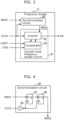
FIG. 3 is a circuit diagram illustrating an example of the configuration offrequency divider 3 inFIG. 1 .FIG. 4 is a circuit diagram illustrating an example of the configuration ofsynchronization circuit 30 inFIG. 3 . - As illustrated in
FIG. 3 ,frequency divider 3 includessynchronization circuit 30 and counter-type frequency divider circuit 31. Counter-type frequency divider circuit 31 includes counter 32 andcomparator 33. -
Synchronization circuit 30 is a circuit that causes reset signal NRST to synchronize with output clock signal VCLK. For this reason,synchronization circuit 30 includes, in the configuration example inFIG. 4 ,inversion circuit 34, flip-flop 35, and flip-flop 36. -
Inversion circuit 34 inverts output clock signal VCLK and outputs the inverted signal to the clock input terminals of flip-flop 35 and flip-flop 36. - Flip-
flop 35 takes in and retains reset signal NRST at the rising edge of the inverted signal from inversion circuit 34 (i.e., at the falling edge of output clock signal VCLK), and outputs the retained signal from the Q output terminal. - Flip-
flop 36 takes in and retains the signal from the Q output terminal of flip-flop 35 at the rising edge of the inverted signal from inversion circuit 34 (i.e., at the falling edge of output clock signal VCLK), and outputs the retained signal from the Q output terminal. The signal output from the Q output terminal of flip-flop 36 is output as counter reset signal NRES to counter 32. Counter reset signal NRES is a signal that delayed reset signal NRST for two clock periods of output clock signal VCLK. Stated differently, counter reset signal NRES is a signal that caused reset signal NRST to synchronize with output clock signal VCLK. - Counter-type frequency divider circuit 31 divides the frequency of output clock signal VCLK at division ratio N and outputs feedback clock signal FB. Counter-type frequency divider circuit 31 in the example in
FIG. 3 includescounter 32 andcomparator 33. -
Counter 32 counts the number of clock pulses of output clock signal VCLK. -
Comparator 33 compares the count value ofcounter 32 and division ratio N, and initializes counter 32 when the count value matches divisionratio N. Comparator 33 determines whether division ratio (N - m) instructed by division ratio setting signal mSET matches the count value when division ratio switching signal CHG is being asserted. m is an integer corresponding to the time difference between the edge timing of reference clock signal REF immediately after switching and the start timing offrequency divider 3 immediately after reset cancel. In the configuration example inFIG. 3 , m denotes the time difference between the rising edge of reset signal NRST and the rising edge of counter reset signal NRES, and corresponds to two clocks of output clock signal VCLK (m = 2). Thus,frequency divider 3 performs frequency division at division ratio (N - m) when division ratio switching signal CHG is being asserted. - Next, the more detailed configuration of
phase comparator 40 will be described. -
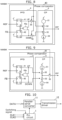
FIG. 5 is a circuit diagram illustrating an example of the configuration ofphase comparator 40 inFIG. 1 .Phase comparator 40 inFIG. 5 includesPFD 4 andCP 5. -
PFD 4 includes flip-flop 41, flip-flop 42, andNAND circuit 43. - Flip-
flop 41 outputs low-level from the Q output terminal in a reset state or immediately after reset cancel. In a state other than a reset state, flip-flop 41 takes in and retains the high-level of the D input terminal at the timing of the rising edge of reference clock signal REF, and also outputs high-level as an UP signal from the Q output terminal. - Flip-
flop 42 outputs low-level from the Q output terminal in a reset state or immediately after reset cancel. Flip-flop 42 takes in and retains the high-level of the D input terminal at the timing of the rising edge of feedback clock signal FB, and also outputs high-level as a DOWN signal from the Q output terminal. -
NAND circuit 43 outputs an output signal obtained by inverting the logical conjunction of the UP signal, the DOWN signal, and mask signal NMSK to the reset input terminal of flip-flop 41 and the reset input terminal of flip-flop 42. When mask signal NMSK is at high-level (i.e., mask signal NBSK is not masked),NAND circuit 43 neither resets flip-flop 41 nor flip-flop 42 when neither the UP signal nor the DOWN signal is at high-level, and resets flip-flop 41 and flip-flop 42 when both of the UP signal and the DOWN signal are at high-level. As a result, when the rising edge of reference clock signal REF is earlier than the rising edge of feedback clock signal FB, a pulse width corresponding to the phase difference between the two signals appears in the UP signal, and a pulse whose duration is short enough to be ignored appears in the DOWN signal. In contrast, when the rising edge of reference clock signal REF is later than the rising edge of feedback clock signal FB, a pulse whose duration is short enough to be ignored appears in the UP signal and a pulse width corresponding to the phase difference between the two signals appears in the DOWN signal. When mask signal NMSK is at low-level, flip-flop 41 and flip-flop 42 are in a reset state. Accordingly, when mask signal NMSK is at low-level, both the UP signal and the DOWN signal are masked. -
CP 5 includescurrent source 51,switch 52,switch 53, andcurrent source 54. -
Current source 51 and switch 52 provide low-pass filter 6 with current ICP in accordance with the pulse width of an UP signal. In this case, current ICP flows fromCP 5 to low-pass filter 6. As a result, the UP signal works to increase the frequency of output clock signal VCLK via low-pass filter 6 and voltage-controlledoscillator 2. -
Switch 53 andcurrent source 54 take out, from low-pass filter 6, current ICP in accordance with the pulse width of a DOWN signal. In this case, current ICP flows from low-pass filter 6 toCP 5. As a result, the DOWN signal works to decrease the frequency of output clock signal VCLK via low-pass filter 6 and voltage-controlledoscillator 2. - The following describes an operation of
PLL circuit 1 according to the embodiment which is configured as described above. - First, an example of an operation performed in
frequency divider 3 will be described. -
FIG. 6 is a time chart illustrating an example of an operation performed infrequency divider 3 inFIG. 3. FIG. 3 illustrates the switching timings of division ratio switching signal CHG, feedback clock signal FB, and a division ratio. It is assumed that the rising edge of feedback clock signal FB occurs at a count start timing to start counting in the frequency division operation. - As indicated at time t0 and time t3, the frequency division operation is started at division ratio N when division ratio switching signal CHG is at low-level at the count start timing.
- As indicated at time t1 and t2, the frequency division operation is started at division ratio (N - m) when division ratio switching signal CHG is at high-level at the count start timing. m is specified by frequency division setting signal mSET.
-
Frequency divider 3 thus switches the division ratio in accordance with the level of division ratio switching signal CHG at the count start timing. - When
frequency divider 3 is reset in the period from time t0 to time t1, the frequency division operation is stopped in the period from time t0 to time t1 and the pulse of feedback clock signal FB is not to be output. - Next, an example of an operation performed in
PLL circuit 1 will be described. -
FIG. 7 is a time chart illustrating an example of an operation performed in a PLL circuit according to the embodiment. - In the period from time t1 to time t5, first clock signal CLK1 is selected and output as reference clock signal REF in
selection circuit 70. In this period, reference clock signal REF and feedback clock signal FB are in a locked state in which the phase of reference clock signal REF matches the phase of feedback clock signal FB, and the UP signal and the DOWN signal each have a pulse width that is short enough to be ignored. - At time t4, the clock switching signal changes from low-level to high-level. In other words, the clock switching signal instructs that reference clock signal REF is to be switched from first clock signal CLK1 to second clock signal CLK2.
- With the change in the clock switching signal,
selection circuit 70 sets the period from time t5 to time t7 as a non-selection period and lowers both first clock selection signal 1SEL and second clock selection signal 2SEL to low-level. - With both first clock selection signal 1SEL and second clock selection signal 2SEL having been changed to low-level at time t5, the output of reference clock signal REF is stopped.
Control circuit 75 changes mask signal NMSK, reset signal NRST, and division ratio switching signal CHG to be active. - In the period from time t5 to time t7, i.e., the non-selection period, reference clock signal REF is not output. At time t7 when second clock selection signal 2SEL is asserted and thereafter, second clock signal CLK2 is selected and output as reference clock signal REF.
- In the period from time t5 to time t10, mask signal NMSK becomes active. During this period, the UP signal and the DOWN signal are both masked in
phase comparator 40 and neither the UP signal nor the DOWN signal is output. As a result, the UP signal indicating the phase difference from time t8 to time t9 is masked. The DOWN signal in the very short period between time t8 and time t9 is also masked. - In the period from time t5 to time t8, reset signal NRST becomes active. With this,
frequency divider 3 stops the frequency division operation. - In the period from time t5 to time t10, division ratio switching signal CHG becomes active. The division ratio of a frequency division operation that is performed by
frequency divider 3 and starts in this period is changed. InFIG. 7 , the division ratio is changed from N to (N - m). - In the period from time t6 to time t9, counter reset signal NRES becomes active. At time t9, counter reset signal NRES becomes inactive and a frequency division operation at division ratio (N - m) starts.
- At time t9, the frequency division operation at ratio (N - m) performed by
frequency divider 3 starts and the rising edge of feedback clock signal FB occurs. Here, m = 2 and m denotes the time difference between the rising edge of reset signal NRST and the rising edge of counter reset signal NRES. Accordingly, at time t11 when the first cycle of the frequency division operation at division ratio (N - m) is completed, the phase difference between reference clock signal REF and feedback clock signal FB gets closer to 0. At this point in time,PLL circuit 1 is in a locked state and frequency fluctuation is inhibited to a large extent. - At time t11, since division ratio switching signal CHG is not active, a frequency division operation at division ratio N starts.
- At time t12, one cycle of the frequency division operation at division ratio N is completed and the phase difference between reference clock signal REF and feedback clock signal FB becomes 0. At this point in time, the locked state of
PLL circuit 1 is maintained and frequency fluctuation is inhibited to a large extent. - Thus, in the operation example in
FIG. 7 , frequency fluctuation at the time of clock switching can be inhibited, as illustrated inFIG. 14 . - The example that applies m = 2 is illustrated in
FIG. 7 , but m = 1 may be applied. In the case of m = 1, the phase difference corresponding to one cycle of output clock signal VCLK remains at time t11 and the phase difference becomes 0 at time t12 inFIG. 7 . Even in this case, sincePLL circuit 1 is in a locked state at time t12, frequency fluctuation can be sufficiently inhibited. In this way, m may correspond to the time difference between the rising edge of reset signal NRST and the rising edge of counter reset signal NRES, or correspond to the duration of a time less than the time difference. -
Phase comparator 40 may be added in the configuration inFIG. 8 or FIG. 9 , instead ofFIG. 5 . InFIG. 5 , mask signal NMSK indirectly masks the UP signal, the DOWN signal, and current ICP by resetting flip-flop 41 and flip-flop 42. InFIG. 8 , mask signal NMSK directly masks the UP signal and the DOWN signal. InFIG. 9 , mask signal NMSK directly masks current ICP. - Next, a transmission system according to the embodiment will be described.
-
FIG. 10 is a block diagram illustrating an example of the configuration of the transmission system according to the embodiment. The transmission system inFIG. 10 includesPLL circuit 1, parallel-serial converter 11, andtransmission driver 12. -
PLL circuit 1 may be configured as inFIG. 1 . For example, one of first clock signal CLK1 and second clock signal CLK2 is a recovery clock and the other of first clock signal CLK1 and second clock signal CLK2 is a clock other than a recovery clock. - Parallel-
serial converter 11 is a shift register that loads and outputs parallel data as serial data in synchronization with output clock signal VCLK fromPLL circuit 1. -
Transmission driver 12 outputs the serial data output from parallel-serial converter 11 to a communication line. - As described above, the PLL circuit according to the embodiment generates an output clock signal and includes: a selection circuit that selects one of a plurality of clock signals as a reference clock signal of the PLL circuit; and a control circuit that when a switch is made for the selection of the reference clock signal, temporarily reduces a division ratio used by a frequency divider that generates a feedback clock signal to be compared with the reference clock signal.
- With the PLL circuit described above, frequency fluctuation of an output clock signal, which is caused by the switching of a reference clock signal, can be inhibited. Temporarily reducing a division ratio temporarily reduces the cycle of a feedback clock signal. For example, when the first edge timing of the feedback clock signal from the frequency divider is little delayed relative to the first edge timing of the reference clock signal immediately after switching, it is possible to match the edge timing of the reference clock signal in the next cycle with the edge timing of the feedback clock signal in the next cycle.
- When the switch is made for the selection of the reference clock signal, the control circuit may temporarily mask a detection result obtained by a phase comparator in the PLL circuit.
- With the above feature, when one of pulses of a reference clock signal and a feedback clock signal is output unnecessarily by mistake, a phase difference due to that unnecessary pulse can be masked. When glitch noise occurs in the reference clock signal at the time of switching for the selection of the reference clock signal, a phase difference due to the glitch noise can be masked. This can inhibit frequency fluctuation at the time of switching for the selection of the reference clock signal.
- A PLL circuit according to the embodiment includes: an oscillator that generates an output clock signal; a frequency divider that divides the frequency of the output clock signal; a phase comparator that detects the phase difference between a reference clock signal and a feedback clock signal output from the frequency divider; a filter circuit that outputs, to the oscillator, a control signal in accordance with the detected phase difference; a selection circuit that selects and outputs, as the reference clock signal, one of a plurality of clock signals to the phase comparator; and a control circuit that when a switch is made for the selection of the reference clock signal, temporarily reduces a division ratio used by the frequency divider.
- With the PLL circuit described above, frequency fluctuation of an output clock signal caused by the switching of a reference clock signal can be inhibited. Temporarily reducing a division ratio temporarily reduces the cycle of a feedback clock signal. For example, when the first edge timing of the feedback clock signal from the frequency divider is little delayed relative to the first edge timing of the reference clock signal immediately after switching, it is possible to match the edge timing of the reference clock signal in the next cycle with the edge timing of the feedback clock signal in the next cycle.
- The control circuit may reset the frequency divider when the switch is made for the selection of the reference clock signal. A period in which the division ratio is temporarily reduced may be a single cycle or a plurality of cycles of the feedback clock signal immediately after reset cancel of the frequency divider.
- With this feature, when the first edge timing of a feedback clock signal from the frequency divider is little delayed relative to the first edge timing of a reference clock signal immediately after switching, for example, an edge timing in the next cycle (or a cycle after few cycles) immediately after reset cancel can be matched between the reference clock signal and the feedback clock signal.
- The control circuit may temporarily change the division ratio from N to (N - m) when the switch is made for the selection of the reference clock signal, where N may be an integer indicating a division ratio in a locked state before the reference clock signal is switched, and m may be an integer corresponding to the time difference between the edge timing of the reference clock signal immediately after the reference clock signal is switched and the start timing of the frequency divider immediately after reset cancel.
- With this feature, edge timing of the feedback clock signal in the next cycle immediately after reset cancel can be matched with the first edge timing of the reference clock signal immediately after switching. As a result, frequency fluctuation can be inhibited to a large extent.
- The control circuit may output a division ratio switching signal to the frequency divider, and the frequency divider may start dividing a frequency at a small division ratio in a period in which the division ratio switching signal is being asserted.
- With this feature, the control of temporarily reducing a division ratio can be readily performed.
- When the switch is made for the selection of the reference clock signal, the control circuit may temporarily mask a signal indicating the phase difference generated by the phase comparator.
- With this feature, when one of pulses of a reference clock signal and a feedback clock signal is unnecessarily output by mistake at the time of switching for the selection of a reference clock signal, a phase difference due to that unnecessary pulse can be masked. When glitch noise occurs in a reference clock signal at the time of switching for the selection of the reference clock signal, a phase difference due to the glitch noise can be masked. This can inhibit frequency fluctuation at the time of switching for the selection of the reference clock signal.
- The control circuit may cancel the masking when the phase difference between the reference clock signal and the feedback clock signal is less than a threshold.
- With this feature, a period in which masking is effective can be optimized.
- The selection circuit may have a stop period during which the selection circuit stops the output of the reference clock signal when the switch is made for the selection of the reference clock signal. The control circuit may bring the frequency divider into a reset state in the stop period and cancel the reset state of the frequency divider at the edge timing of the reference clock signal, where the edge timing occurs when the stop period is ended.
- With this feature, unnecessary output of a reference clock signal can be prevented at the time of switching for the selection of the reference clock signal owing to a stop period and reset cancel, which in turn makes it possible to reduce the factors of frequency fluctuation.
- The selection circuit may not output glitch noise when the switch is made for the selection of the reference clock signal.
- With this feature, glitch noise that causes frequency fluctuation can be reduced at the time of switching for the selection of the reference clock signal.
- A transmission system according to the embodiment includes: the above-described PLL circuit; a converter that converts parallel data into serial data in synchronization with the output clock signal; and a transmission driver that outputs the serial data to a communication line.
- In the above-described embodiment, each of elements may be implemented by dedicated hardware or by executing a software program suitable for the element. Each of the elements may be implemented by a program executor such as a CPU or a processor reading and executing a software program recorded on, for instance, a semiconductor memory.
- Although the PLL circuit and transmission system according to one or more aspects of the present disclosure have been described based on an embodiment, the present disclosure is not limited to the embodiment. Other embodiments obtained by various modifications of the embodiments that may be conceived by persons skilled in the art, as well as embodiments resulting from arbitrary combinations of elements from different embodiments that do not depart from the essence of the present disclosure are also included in one or more aspects of the present disclosure.
- The present disclosure is applicable to a PLL circuit that can switch a reference clock signal.
-
- 1
- PLL circuit
- 2
- voltage-controlled oscillator
- 3
- frequency divider
- 4
- PFD
- 5
- CP
- 6
- low-pass filter
- 7
- switching circuit
- 11
- parallel-serial converter
- 12
- transmission driver
- 30
- synchronization circuit
- 31
- counter-type frequency divider circuit
- 32
- counter
- 33
- comparator
- 34
- inversion circuit
- 35, 36, 41, 42, 77, 78
- flip-flop
- 40
- phase comparator
- 43, 43a
- NAND circuit
- 44, 45, 52, 53, 55
- switch
- 51, 54
- current source
- 70
- selection circuit
- 71
- logic circuit
- 72, 73
- AND circuit
- 74
- OR circuit
- 75
- control circuit
- 76
- XOR circuit
- 79
- inversion circuit
Claims (11)
- A phase-locked loop (PLL) circuit that generates an output clock signal, the PLL circuit comprising:a selection circuit that selects one of a plurality of clock signals as a reference clock signal of the PLL circuit; anda control circuit that when a switch is made for the selection of the reference clock signal, temporarily reduces a division ratio used by a frequency divider that generates a feedback clock signal to be compared with the reference clock signal.
- The PLL circuit according to claim 1, wherein
when the switch is made for the selection of the reference clock signal, the control circuit temporarily masks a detection result obtained by a phase comparator in the PLL circuit. - A phase-locked loop (PLL) circuit comprising:an oscillator that generates an output clock signal;a frequency divider that divides a frequency of the output clock signal;a phase comparator that detects a phase difference between a reference clock signal and a feedback clock signal output from the frequency divider;a filter circuit that outputs, to the oscillator, a control signal in accordance with the phase difference detected;a selection circuit that selects and outputs, as the reference clock signal, one of a plurality of clock signals to the phase comparator; anda control circuit that when a switch is made for the selection of the reference clock signal, temporarily reduces a division ratio used by the frequency divider.
- The PLL circuit according to any one of claims 1 to 3, whereinthe control circuit resets the frequency divider when the switch is made for the selection of the reference clock signal, anda period in which the division ratio is temporarily reduced is a single cycle or a plurality of cycles of the feedback clock signal immediately after reset cancel of the frequency divider.
- The PLL circuit according to any one of claims 1 to 4, wherein
the control circuit temporarily changes the division ratio from N to (N - m) when the switch is made for the selection of the reference clock signal, where N is an integer indicating a division ratio in a locked state before the reference clock signal is switched, and m is an integer corresponding to a time difference between an edge timing of the reference clock signal immediately after the reference clock signal is switched and a start timing of the frequency divider immediately after reset cancel. - The PLL circuit according to any one of claims 1 to 5, whereinthe control circuit outputs a division ratio switching signal to the frequency divider, andthe frequency divider starts dividing a frequency at a small division ratio in a period in which the division ratio switching signal is being asserted.
- The PLL circuit according to claim 3, wherein
when the switch is made for the selection of the reference clock signal, the control circuit temporarily masks a signal indicating the phase difference generated by the phase comparator. - The PLL circuit according to claim 2 or 7, wherein
the control circuit cancels the masking when a phase difference between the reference clock signal and the feedback clock signal is less than a threshold. - The PLL circuit according to any one of claims 1 to 8, whereinthe selection circuit has a stop period during which the selection circuit does not output the reference clock signal when the switch is made for the selection of the reference clock signal, andthe control circuit brings the frequency divider into a reset state in the stop period and cancels the reset state of the frequency divider at an edge timing of the reference clock signal, the edge timing occurring when the stop period is ended.
- The PLL circuit according to any one of claims 1 to 9, wherein
the selection circuit does not output glitch noise when the switch is made for the selection of the reference clock signal. - A transmission system comprising:the PLL circuit according to any one of claims 1 to 10;a converter that converts parallel data into serial data in synchronization with the output clock signal; anda transmission driver that outputs the serial data to a communication line.
Applications Claiming Priority (2)
| Application Number | Priority Date | Filing Date | Title |
|---|---|---|---|
| JP2021137169 | 2021-08-25 | ||
| PCT/JP2022/031746 WO2023027078A1 (en) | 2021-08-25 | 2022-08-23 | Pll circuit and transmission system |
Publications (2)
| Publication Number | Publication Date |
|---|---|
| EP4395178A1 true EP4395178A1 (en) | 2024-07-03 |
| EP4395178A4 EP4395178A4 (en) | 2024-12-25 |
Family
ID=85322853
Family Applications (1)
| Application Number | Title | Priority Date | Filing Date |
|---|---|---|---|
| EP22861366.7A Pending EP4395178A4 (en) | 2021-08-25 | 2022-08-23 | PLL CIRCUIT AND TRANSMISSION SYSTEM |
Country Status (6)
| Country | Link |
|---|---|
| US (1) | US12401367B2 (en) |
| EP (1) | EP4395178A4 (en) |
| JP (1) | JP7818608B2 (en) |
| CN (1) | CN117837087A (en) |
| TW (1) | TW202318808A (en) |
| WO (1) | WO2023027078A1 (en) |
Cited By (1)
| Publication number | Priority date | Publication date | Assignee | Title |
|---|---|---|---|---|
| US20240187006A1 (en) * | 2021-08-25 | 2024-06-06 | Nuvoton Technology Corporation Japan | Pll circuit and transmission system |
Families Citing this family (5)
| Publication number | Priority date | Publication date | Assignee | Title |
|---|---|---|---|---|
| US12542547B2 (en) * | 2024-02-26 | 2026-02-03 | International Business Machines Corporation | Reducing the time to switch between the redundant clock signals applied to a phase lock loop |
| EP4629512A1 (en) * | 2024-04-02 | 2025-10-08 | Nxp B.V. | Phase-locked loop reference clock switching with controlled output transient frequency drift |
| TWI869261B (en) * | 2024-04-10 | 2025-01-01 | 新唐科技股份有限公司 | Method for reducing influence of noise on signal line and decoding circuit using the same |
| CN118590041A (en) * | 2024-06-20 | 2024-09-03 | 中国电子科技集团公司第十研究所 | A digital integrated circuit clock reset system |
| WO2026090096A1 (en) * | 2024-10-23 | 2026-04-30 | Texas Instruments Incorporated | Methods and apparatus to maintain a phase lock during a frequency change |
Family Cites Families (78)
| Publication number | Priority date | Publication date | Assignee | Title |
|---|---|---|---|---|
| SU1293841A1 (en) * | 1984-10-09 | 1987-02-28 | Предприятие П/Я В-8574 | Frequency synthesizer |
| US4823363A (en) * | 1985-07-09 | 1989-04-18 | Nec Corporation | Phase-locked clock regeneration circuit for digital transmission systems |
| US4864253A (en) * | 1987-12-22 | 1989-09-05 | Siemens Aktiengesellschaft | Phase locked loop wherein phase comparing and filtering are performed by microprocessor |
| GB2223136B (en) * | 1988-03-28 | 1992-10-14 | Plessey Co Plc | Broad band vco control system for clock recovery |
| JP2589370B2 (en) * | 1989-04-13 | 1997-03-12 | シャープ株式会社 | Optical disk drive |
| JPH0327620A (en) * | 1989-06-23 | 1991-02-06 | Fujitsu Ltd | Switching device for reference signal |
| JPH06152581A (en) * | 1992-11-10 | 1994-05-31 | Fujitsu Ltd | Clock supply device |
| JP3313175B2 (en) * | 1993-02-19 | 2002-08-12 | 富士通株式会社 | Apparatus and method for detecting servo position of disk drive |
| US6269061B1 (en) * | 1993-10-07 | 2001-07-31 | Sony Corporation | Servo control system for disk player |
| CN1031846C (en) * | 1993-11-20 | 1996-05-22 | 南京理工大学 | Basic colour gradation grading sequence addressing dynamic image display screen |
| JPH0818447A (en) * | 1994-06-28 | 1996-01-19 | Mitsubishi Electric Corp | PLL circuit device |
| GB2293062B (en) * | 1994-09-09 | 1996-12-04 | Toshiba Kk | Master-slave multiplex communication system and PLL circuit applied to the system |
| JP2606670B2 (en) * | 1994-09-29 | 1997-05-07 | 日本電気株式会社 | Optical disc playback device |
| JP3260048B2 (en) * | 1994-12-13 | 2002-02-25 | 株式会社東芝 | Clock signal generation circuit and semiconductor device |
| JPH08228149A (en) * | 1995-02-22 | 1996-09-03 | Toshiba Corp | Phase locked loop circuit |
| JPH0983396A (en) * | 1995-09-07 | 1997-03-28 | Sony Corp | Receiving machine |
| US6141769A (en) * | 1996-05-16 | 2000-10-31 | Resilience Corporation | Triple modular redundant computer system and associated method |
| JPH1013383A (en) * | 1996-06-26 | 1998-01-16 | Matsushita Electric Ind Co Ltd | Optical transmission system |
| JPH1022822A (en) * | 1996-07-05 | 1998-01-23 | Sony Corp | Digital PLL circuit |
| JP3591754B2 (en) * | 1997-03-19 | 2004-11-24 | パイオニア株式会社 | PLL circuit |
| TW419901B (en) * | 1997-06-27 | 2001-01-21 | Hitachi Ltd | Phase-locked ring circuit, data processing device and data process system |
| US6341149B1 (en) * | 1997-06-27 | 2002-01-22 | International Business Machines Corporation | Clock control device for a non-disruptive backup clock switching |
| US5907263A (en) * | 1997-11-14 | 1999-05-25 | Cirrus Logic, Inc. | Bias current calibration of voltage controlled oscillator |
| US6182236B1 (en) * | 1998-08-26 | 2001-01-30 | Compaq Computer Corporation | Circuit and method employing feedback for driving a clocking signal to compensate for load-induced skew |
| JP3085293B2 (en) * | 1998-11-18 | 2000-09-04 | 日本電気株式会社 | Data transmission equipment |
| US6208183B1 (en) * | 1999-04-30 | 2001-03-27 | Conexant Systems, Inc. | Gated delay-locked loop for clock generation applications |
| FR2793091B1 (en) * | 1999-04-30 | 2001-06-08 | France Telecom | FREQUENCY SERVO DEVICE |
| JP2001094420A (en) * | 1999-09-24 | 2001-04-06 | Fujitsu Ltd | Phase locked loop circuit |
| US6259328B1 (en) * | 1999-12-17 | 2001-07-10 | Network Equipment Technologies, Inc. | Method and system for managing reference signals for network clock synchronization |
| US6362670B1 (en) * | 2000-08-04 | 2002-03-26 | Marconi Communications, Inc. | Controlled slew reference switch for a phase locked loop |
| US6307411B1 (en) * | 2000-10-13 | 2001-10-23 | Brookhaven Science Associates | Wide tracking range, auto ranging, low jitter phase lock loop for swept and fixed frequency systems |
| JP3557612B2 (en) * | 2000-12-05 | 2004-08-25 | 日本電気株式会社 | Low latency high speed transmission system |
| JP3655878B2 (en) | 2002-02-18 | 2005-06-02 | 埼玉日本電気株式会社 | PLL circuit |
| JP2004015659A (en) * | 2002-06-10 | 2004-01-15 | Mitsubishi Electric Corp | PLL controller |
| EP1376526A3 (en) * | 2002-06-26 | 2004-12-08 | Pioneer Corporation | Display panel drive device, data transfer system and data reception device |
| JP2004037939A (en) * | 2002-07-04 | 2004-02-05 | Pioneer Electronic Corp | Display panel driver, display controller, driver, and data transfer system |
| JP2004364366A (en) * | 2003-06-02 | 2004-12-24 | Seiko Epson Corp | PWM control system |
| GB0323936D0 (en) * | 2003-10-11 | 2003-11-12 | Zarlink Semiconductor Inc | Digital phase locked loop with selectable normal or fast-locking capability |
| JP2005252587A (en) * | 2004-03-03 | 2005-09-15 | Seiko Epson Corp | Clock shaper and electronic device using clock shaper |
| JP2005277880A (en) * | 2004-03-25 | 2005-10-06 | Seiko Epson Corp | Clock shaper and electronic device using the same |
| JP4651348B2 (en) | 2004-09-30 | 2011-03-16 | 株式会社タムラ製作所 | Digital audio adjustment device |
| JP2007049217A (en) * | 2005-08-05 | 2007-02-22 | Matsushita Electric Ind Co Ltd | Network system |
| JP2007266923A (en) * | 2006-03-28 | 2007-10-11 | Fujitsu Ltd | Clock supply device |
| US7902886B2 (en) * | 2007-10-30 | 2011-03-08 | Diablo Technologies Inc. | Multiple reference phase locked loop |
| US7737739B1 (en) * | 2007-12-12 | 2010-06-15 | Integrated Device Technology, Inc. | Phase step clock generator |
| US8077822B2 (en) * | 2008-04-29 | 2011-12-13 | Qualcomm Incorporated | System and method of controlling power consumption in a digital phase locked loop (DPLL) |
| JP2011170644A (en) * | 2010-02-19 | 2011-09-01 | Sony Corp | Communication device, communication system, and communication method |
| JP5560833B2 (en) * | 2010-03-29 | 2014-07-30 | 富士通株式会社 | Optical interface device and input frequency deviation abnormality monitoring method |
| US8222933B2 (en) * | 2010-05-07 | 2012-07-17 | Texas Instruments Incorporated | Low power digital phase lock loop circuit |
| US8395428B2 (en) * | 2010-09-30 | 2013-03-12 | St-Ericsson Sa | Reference clock sampling digital PLL |
| JP5711949B2 (en) * | 2010-12-03 | 2015-05-07 | ローム株式会社 | Serial data reception circuit, reception method, serial data transmission system using the same, and transmission method |
| US20120166859A1 (en) * | 2010-12-22 | 2012-06-28 | Fernald Kenneth W | Method and apparatus for generating a system clock signal |
| WO2012150621A1 (en) * | 2011-05-02 | 2012-11-08 | パナソニック株式会社 | Frequency synthesizer |
| US8842490B2 (en) * | 2012-06-29 | 2014-09-23 | Intel Corporation | Apparatus and method for selectively using a memory command clock as a reference clock |
| US9343126B2 (en) * | 2012-09-12 | 2016-05-17 | Intel Corporation | Frequency selection granularity for integrated circuits |
| JP2014158195A (en) * | 2013-02-18 | 2014-08-28 | Renesas Electronics Corp | Wireless communication system and semiconductor device for wireless communication |
| US9142272B2 (en) * | 2013-03-15 | 2015-09-22 | International Business Machines Corporation | Dual asynchronous and synchronous memory system |
| CN203387495U (en) * | 2013-08-14 | 2014-01-08 | 江西航天海虹测控技术有限责任公司 | PLL (Phase Locked Loop) circuit reference clock switching circuit system |
| US9395745B2 (en) * | 2014-02-10 | 2016-07-19 | Analog Devices, Inc. | Redundant clock switchover |
| US9531390B1 (en) * | 2015-12-15 | 2016-12-27 | Altera Corporation | Techniques for generating clock signals using oscillators |
| US10523219B2 (en) * | 2016-03-04 | 2019-12-31 | Sony Corporation | Phase locked loop and control method therefor |
| JP2018011277A (en) * | 2016-07-15 | 2018-01-18 | 富士通株式会社 | Transmission apparatus and clock control method |
| KR102367235B1 (en) * | 2016-08-30 | 2022-02-23 | 가부시키가이샤 한도오따이 에네루기 켄큐쇼 | A receiver for receiving a differential signal, an IC including the receiver, and a display device |
| KR102757627B1 (en) * | 2016-09-23 | 2025-01-23 | 삼성전자주식회사 | Electronic device comprising storage devices transmitting reference clock via cascade coupling structure |
| WO2018096973A1 (en) * | 2016-11-28 | 2018-05-31 | パナソニックIpマネジメント株式会社 | Pulse frequency control circuit, microcontroller, dc-dc converter, and pulse frequency control method |
| US10234895B2 (en) * | 2017-05-11 | 2019-03-19 | Microsemi Semiconductor Ulc | Clock synthesizer with hitless reference switching and frequency stabilization |
| US10516402B2 (en) * | 2018-03-09 | 2019-12-24 | Texas Instruments Incorporated | Corrupted clock detection circuit for a phase-locked loop |
| US10491222B2 (en) * | 2018-03-13 | 2019-11-26 | Texas Instruments Incorporated | Switch between input reference clocks of different frequencies in a phase locked loop (PLL) without phase impact |
| JP2019204998A (en) * | 2018-05-21 | 2019-11-28 | 株式会社デンソー | PLL circuit |
| US11152947B2 (en) * | 2019-02-20 | 2021-10-19 | Renesas Electronics America Inc. | Feedback control for accurate signal generation |
| US10790838B1 (en) * | 2019-05-14 | 2020-09-29 | Intel Corporation | Method and apparatus to perform dynamic frequency scaling while a phase-locked loop operates in a closed loop |
| US10727845B1 (en) * | 2019-06-25 | 2020-07-28 | Silicon Laboratories Inc. | Use of a virtual clock in a PLL to maintain a closed loop system |
| JP7113788B2 (en) * | 2019-07-01 | 2022-08-05 | 三菱電機株式会社 | Phase lock circuit |
| WO2021112000A1 (en) * | 2019-12-05 | 2021-06-10 | ローム株式会社 | Pll circuit and control method for same |
| KR102955918B1 (en) * | 2019-12-13 | 2026-04-21 | 삼성전자주식회사 | Clock recovery circuit, clock data recovery circuit, and apparatus including the same |
| US11031945B1 (en) * | 2020-09-11 | 2021-06-08 | Apple Inc. | Time-to-digital converter circuit linearity test mechanism |
| WO2023027078A1 (en) * | 2021-08-25 | 2023-03-02 | ヌヴォトンテクノロジージャパン株式会社 | Pll circuit and transmission system |
| CN118801874A (en) * | 2024-07-25 | 2024-10-18 | 思瑞浦微电子科技(上海)有限责任公司 | Dual-mode clock system and mode switching method |
-
2022
- 2022-08-23 WO PCT/JP2022/031746 patent/WO2023027078A1/en not_active Ceased
- 2022-08-23 CN CN202280057066.7A patent/CN117837087A/en active Pending
- 2022-08-23 JP JP2023543935A patent/JP7818608B2/en active Active
- 2022-08-23 EP EP22861366.7A patent/EP4395178A4/en active Pending
- 2022-08-24 TW TW111131890A patent/TW202318808A/en unknown
-
2024
- 2024-02-14 US US18/441,724 patent/US12401367B2/en active Active
Cited By (2)
| Publication number | Priority date | Publication date | Assignee | Title |
|---|---|---|---|---|
| US20240187006A1 (en) * | 2021-08-25 | 2024-06-06 | Nuvoton Technology Corporation Japan | Pll circuit and transmission system |
| US12401367B2 (en) * | 2021-08-25 | 2025-08-26 | Nuvoton Technology Corporation Japan | PLL circuit and transmission system |
Also Published As
| Publication number | Publication date |
|---|---|
| TW202318808A (en) | 2023-05-01 |
| US12401367B2 (en) | 2025-08-26 |
| US20240187006A1 (en) | 2024-06-06 |
| JPWO2023027078A1 (en) | 2023-03-02 |
| EP4395178A4 (en) | 2024-12-25 |
| JP7818608B2 (en) | 2026-02-20 |
| CN117837087A (en) | 2024-04-05 |
| WO2023027078A1 (en) | 2023-03-02 |
Similar Documents
| Publication | Publication Date | Title |
|---|---|---|
| US12401367B2 (en) | PLL circuit and transmission system | |
| US7073098B2 (en) | Multi-phase clock generation circuit and clock multiplication circuit | |
| US20200266806A1 (en) | Fractional frequency divider and frequency synthesizer | |
| CN112165327A (en) | Locking detection circuit and display device | |
| US6864729B2 (en) | Mode switching method for PLL circuit and mode control circuit for PLL circuit | |
| US6670834B1 (en) | Digital lock detect for dithering phase lock loops | |
| US20110133795A1 (en) | Digital phase-locked loop with reduced loop delay | |
| US20140103961A1 (en) | Phase frequency detector circuit | |
| JPH11205134A (en) | Lock detection circuit and PLL frequency synthesizer | |
| US6954510B2 (en) | Phase-locked loop lock detector circuit and method of lock detection | |
| JP2001028542A (en) | Pll circuit | |
| JP2006191372A (en) | Dual loop PLL and multiplying clock generator | |
| JP3983575B2 (en) | Frequency comparator and lock detection circuit using the same | |
| JP2002198807A (en) | Pll circuit and optical communication receiver | |
| JP2008131353A (en) | PLL lock detection circuit and semiconductor device | |
| JP3250151B2 (en) | Jitter suppression circuit | |
| JP2001021596A (en) | Binary signal comparison device and PLL circuit using the same | |
| JP6435683B2 (en) | PLL circuit and semiconductor integrated circuit | |
| JP2000286703A (en) | Reset circuit and PLL frequency synthesizer | |
| JP2008060895A (en) | Phase-locked circuit | |
| KR101017633B1 (en) | Noise Reduction Method of Low Noise Voltage Controlled Oscillator and Voltage Controlled Oscillator | |
| JP3079943B2 (en) | PLL circuit | |
| JP4718387B2 (en) | Frequency comparison circuit, PLL frequency synthesizer test circuit, and test method therefor | |
| JP2830297B2 (en) | PLL circuit | |
| US12633928B2 (en) | Clock signal frequency divider, processing system, processing device, and clock signal frequency dividing method |
Legal Events
| Date | Code | Title | Description |
|---|---|---|---|
| STAA | Information on the status of an ep patent application or granted ep patent |
Free format text: STATUS: THE INTERNATIONAL PUBLICATION HAS BEEN MADE |
|
| PUAI | Public reference made under article 153(3) epc to a published international application that has entered the european phase |
Free format text: ORIGINAL CODE: 0009012 |
|
| STAA | Information on the status of an ep patent application or granted ep patent |
Free format text: STATUS: REQUEST FOR EXAMINATION WAS MADE |
|
| 17P | Request for examination filed |
Effective date: 20240216 |
|
| AK | Designated contracting states |
Kind code of ref document: A1 Designated state(s): AL AT BE BG CH CY CZ DE DK EE ES FI FR GB GR HR HU IE IS IT LI LT LU LV MC MK MT NL NO PL PT RO RS SE SI SK SM TR |
|
| REG | Reference to a national code |
Ref country code: DE Ref legal event code: R079 Free format text: PREVIOUS MAIN CLASS: H03L0007080000 Ipc: H03L0007140000 |
|
| DAV | Request for validation of the european patent (deleted) | ||
| DAX | Request for extension of the european patent (deleted) | ||
| A4 | Supplementary search report drawn up and despatched |
Effective date: 20241122 |
|
| RIC1 | Information provided on ipc code assigned before grant |
Ipc: H03K 5/1252 20060101ALI20241118BHEP Ipc: H03L 7/195 20060101ALI20241118BHEP Ipc: H03L 7/089 20060101ALI20241118BHEP Ipc: H03L 7/14 20060101AFI20241118BHEP |