EP4394433A1 - Radarvorrichtung und verstärkungseinstellungsverfahren - Google Patents
Radarvorrichtung und verstärkungseinstellungsverfahren Download PDFInfo
- Publication number
- EP4394433A1 EP4394433A1 EP22860846.9A EP22860846A EP4394433A1 EP 4394433 A1 EP4394433 A1 EP 4394433A1 EP 22860846 A EP22860846 A EP 22860846A EP 4394433 A1 EP4394433 A1 EP 4394433A1
- Authority
- EP
- European Patent Office
- Prior art keywords
- signal
- amplitude
- module
- maximum value
- quadrature
- Prior art date
- Legal status (The legal status is an assumption and is not a legal conclusion. Google has not performed a legal analysis and makes no representation as to the accuracy of the status listed.)
- Pending
Links
Images



Classifications
-
- G—PHYSICS
- G01—MEASURING; TESTING
- G01S—RADIO DIRECTION-FINDING; RADIO NAVIGATION; DETERMINING DISTANCE OR VELOCITY BY USE OF RADIO WAVES; LOCATING OR PRESENCE-DETECTING BY USE OF THE REFLECTION OR RERADIATION OF RADIO WAVES; ANALOGOUS ARRANGEMENTS USING OTHER WAVES
- G01S7/00—Details of systems according to groups G01S13/00, G01S15/00, G01S17/00
- G01S7/02—Details of systems according to groups G01S13/00, G01S15/00, G01S17/00 of systems according to group G01S13/00
- G01S7/35—Details of non-pulse systems
- G01S7/352—Receivers
- G01S7/358—Receivers using I/Q processing
-
- G—PHYSICS
- G01—MEASURING; TESTING
- G01S—RADIO DIRECTION-FINDING; RADIO NAVIGATION; DETERMINING DISTANCE OR VELOCITY BY USE OF RADIO WAVES; LOCATING OR PRESENCE-DETECTING BY USE OF THE REFLECTION OR RERADIATION OF RADIO WAVES; ANALOGOUS ARRANGEMENTS USING OTHER WAVES
- G01S7/00—Details of systems according to groups G01S13/00, G01S15/00, G01S17/00
- G01S7/02—Details of systems according to groups G01S13/00, G01S15/00, G01S17/00 of systems according to group G01S13/00
- G01S7/35—Details of non-pulse systems
- G01S7/352—Receivers
-
- G—PHYSICS
- G01—MEASURING; TESTING
- G01S—RADIO DIRECTION-FINDING; RADIO NAVIGATION; DETERMINING DISTANCE OR VELOCITY BY USE OF RADIO WAVES; LOCATING OR PRESENCE-DETECTING BY USE OF THE REFLECTION OR RERADIATION OF RADIO WAVES; ANALOGOUS ARRANGEMENTS USING OTHER WAVES
- G01S7/00—Details of systems according to groups G01S13/00, G01S15/00, G01S17/00
- G01S7/02—Details of systems according to groups G01S13/00, G01S15/00, G01S17/00 of systems according to group G01S13/00
- G01S7/03—Details of HF subsystems specially adapted therefor, e.g. common to transmitter and receiver
- G01S7/038—Feedthrough nulling circuits
-
- G—PHYSICS
- G01—MEASURING; TESTING
- G01S—RADIO DIRECTION-FINDING; RADIO NAVIGATION; DETERMINING DISTANCE OR VELOCITY BY USE OF RADIO WAVES; LOCATING OR PRESENCE-DETECTING BY USE OF THE REFLECTION OR RERADIATION OF RADIO WAVES; ANALOGOUS ARRANGEMENTS USING OTHER WAVES
- G01S13/00—Systems using the reflection or reradiation of radio waves, e.g. radar systems; Analogous systems using reflection or reradiation of waves whose nature or wavelength is irrelevant or unspecified
- G01S13/88—Radar or analogous systems specially adapted for specific applications
- G01S13/93—Radar or analogous systems specially adapted for specific applications for anti-collision purposes
- G01S13/937—Radar or analogous systems specially adapted for specific applications for anti-collision purposes of marine craft
-
- G—PHYSICS
- G01—MEASURING; TESTING
- G01S—RADIO DIRECTION-FINDING; RADIO NAVIGATION; DETERMINING DISTANCE OR VELOCITY BY USE OF RADIO WAVES; LOCATING OR PRESENCE-DETECTING BY USE OF THE REFLECTION OR RERADIATION OF RADIO WAVES; ANALOGOUS ARRANGEMENTS USING OTHER WAVES
- G01S7/00—Details of systems according to groups G01S13/00, G01S15/00, G01S17/00
- G01S7/02—Details of systems according to groups G01S13/00, G01S15/00, G01S17/00 of systems according to group G01S13/00
- G01S7/35—Details of non-pulse systems
- G01S7/352—Receivers
- G01S7/354—Extracting wanted echo-signals
-
- G—PHYSICS
- G01—MEASURING; TESTING
- G01S—RADIO DIRECTION-FINDING; RADIO NAVIGATION; DETERMINING DISTANCE OR VELOCITY BY USE OF RADIO WAVES; LOCATING OR PRESENCE-DETECTING BY USE OF THE REFLECTION OR RERADIATION OF RADIO WAVES; ANALOGOUS ARRANGEMENTS USING OTHER WAVES
- G01S7/00—Details of systems according to groups G01S13/00, G01S15/00, G01S17/00
- G01S7/02—Details of systems according to groups G01S13/00, G01S15/00, G01S17/00 of systems according to group G01S13/00
- G01S7/40—Means for monitoring or calibrating
- G01S7/4004—Means for monitoring or calibrating of parts of a radar system
- G01S7/4021—Means for monitoring or calibrating of parts of a radar system of receivers
Definitions
- the present invention relates to a radar apparatus (device) and gain adjustment method.
- Patent Document 1 Japanese Patent Application Laid-Open No. 2001 -228240 discloses a received signal amplifier as follows. That is, in the received signal amplifier of an FMCW radar which transmits radio waves and receives reflected waves from a target to obtain a distance to the target or a relative speed to the target, the received signal amplifier includes a plurality of amplifiers connected in tandem to amplify a received signal, and an output selection means which selects an amplifier whose output voltage matches the input voltage range of the A/D conversion means and whose level is the highest among the amplifiers and guides the output to the A/D conversion means.
- Patent Literature 1 Japanese Patent Laid-Open No. 2001-228240
- the gain of the received signal is adjusted by selectively using one or more amplifiers from among a plurality of amplifiers, and it is difficult to finely adjust the gain of the received signal.
- the gain of the received signal in which the gain of the received signal is controlled by using an AGC (Auto Gain Control) circuit, the gain of the received signal may not be adjusted appropriately. If the gain of the received signal cannot be adjusted appropriately, for example, the strength of the received signal after adjustment of the gain may be excessively large. Beyond such conventional techniques, it is desirable to have a technique capable of more appropriately adjusting the gain of the received signal.
- the display processing module 202 Based on the plurality of echo data received from the radar module 201, the display processing module 202 performs processing to display the echo image in the detected target area on the display module.
- An A/D conversion module 180 digitally converts the I signal Si and the Q signal Sq. That is, the A/D conversion module 180 converts the analog beat signal Sbb received from the frequency conversion module 170 into a beat signal SD which is a digital signal consisting of a set of the I signal Si and the Q signal Sq. More specifically, the A/D conversion module 180 generates N beat signals SD consisting of a set of N I signals Si and N Q signals Sq by sampling at a predetermined sampling frequency every sweep period T, and outputs them to the signal processing module 190.
- N is an integer of 2 or more.
- the signal processing module 190 then performs processing such as window function processing and FFT processing on the beat signal SD converted to a real signal voltage to generate a power spectrum.
- the signal processing module 190 multiplies the frequency in the generated power spectrum by a predetermined coefficient C to convert the frequency into a distance, thereby generating amplitude data DS.
- the signal processing module 190 generates echo data by logarithmically converting the absolute value of the generated amplitude data DS, and outputs the generated echo data to the display processing module 202.
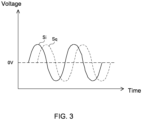
- FIG. 3 is a diagram showing an example of a signal received by an amplitude signal generating module in a radar apparatus according to an embodiment of the present invention.
- a solid line indicates an I signal Si
- a dashed line indicates a Q signal Sq.
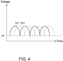
- FIG. 4 is a diagram showing an example of a signal output by an amplitude signal generating module in a radar apparatus according to an embodiment of the present invention.
- a solid line indicates an amplitude signal Smi
- a dashed line indicates an amplitude signal Smq.
- the radar module 201 may have an offset applying circuit (not shown).
- the offset applying circuit receives the I signal Si and the Q signal Sq output from the frequency conversion module 170, applies a predetermined level of offset voltage Vo to the received I signal Si and the Q signal Sq, and outputs the offset voltage Vo to the adjustment module 100 and the A/D conversion module 180.
- a unipolar A/D conversion module can be used as the A/D conversion module 180.
- the maximum value selecting module 20 selects the higher level of the amplitude signal Smi and the amplitude signal Smq as the maximum value signal Smax.
- FIG. 6 is a diagram showing an example of a maximum value signal output by the LPF in a radar apparatus according to an embodiment of the present invention.
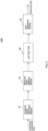
- the gain adjustment module 40 adjusts the gain of the received signal based on the maximum value signal Smax. For example, the gain of the received signal is adjusted based on the maximum value signal Fmax passed through the LPF 30.
- the gain adjustment module 40 generates a control voltage corresponding to the level of the maximum value signal Fmax received from the LPF 30, and outputs the generated control voltage to a variable gain amplifier in the reception module 150.
- the gain adjustment module 40 includes an integrator using an operational amplifier.
- a maximum value signal Fmax is inputted to the non-inverting input terminal
- a reference voltage Vref of a predetermined level is inputted to the inverting input terminal
- a control voltage is outputted from the output terminal.
- the reference voltage Vref is preset based on the dynamic range of the A/D conversion module 180.
- FIG. 7 is a diagram showing an example of a signal output by the frequency conversion module in a radar apparatus according to an embodiment of the present invention.
- a solid line indicates the I signal Si output from the frequency conversion module 170 to the A/D conversion module 180 in the radar apparatus 300
- a dashed line indicates the I signal Sic output from the frequency conversion module 170 to the A/D conversion module 180 in a radar apparatus without the adjustment module 100.
- a beat signal Sbb not conforming to the dynamic range of the A/D conversion module 180 may be output from the frequency conversion module 170 to the A/D conversion module 180 due to an increase in the level of the received signal received via the reception antenna 140.
- the level of the beat signal Sbb output from the frequency conversion module 170 to the A/D conversion module 180 converges to the level of the reference voltage Vref. Therefore, even when the level of the received signal increases, the level of the beat signal Sbb output from the frequency conversion module 170 to the A/D conversion module 180 can be adjusted so as to conform to the dynamic range of the A/D conversion module 180.
- FIG. 8 is a diagram showing an example of a circuit configuration of an adjustment module in a radar apparatus according to an embodiment of the present invention.
- FIG. 8 shows a circuit configuration of an amplitude signal generation module 10, a maximum value selection module 20, and an LPF 30.
- the input terminal T1 receives the I signal Si output from the frequency conversion module 170.
- the input terminal T2 receives the Q signal Sq output from the frequency conversion module 170.
- the output terminal T3 outputs the maximum value signal Fmax to the gain adjustment module 40.
- the input terminal T1 is connected to the first end of the resistor R1.
- the input terminal T2 is connected to the first end of the resistor R6.
- the second end of the resistor R1, the first end of the resistor R2, the inverted input terminal of the operational amplifier OP1, and the first end of the resistor R3 are connected.
- the non-inverted input terminal of the operational amplifier OP1 and the ground are connected.
- the second end of the resistor R2, the first end of the resistor R4 and the anode of the diode D1 are connected.
- a cathode of the diode D1, an output terminal of the operational amplifier OP1, and an anode of the diode D2 are connected.
- a second end of the resistor R4, a first end of the resistor R5, and an inverted input terminal of the operational amplifier OP2 are connected.
- a second end of the resistor R3, a cathode of the diode D2, and a non-inverted input terminal of the operational amplifier OP2 are connected.
- An output terminal of the operational amplifier OP2 and an anode of the diode D3 are connected.
- a second end of the resistor R6, a first end of the resistor R7, an inverted input terminal of the operational amplifier OP3, and a first end of the resistor R8 are connected.
- a non-inverted input terminal of the operational amplifier OP3 and a ground are connected.
- a second end of the resistor R7, a first end of the resistor R9 and an anode of the diode D4 are connected.
- a cathode of the diode D4, an output terminal of the operational amplifier OP3 and an anode of the diode D5 are connected.
- a second end of the resistor R9, a first end of the resistor R10 and an inverted input terminal of the operational amplifier OP4 are connected.
- the second end of the resistor R5, the cathode of the diode D3, the second end of the resistor R10, the cathode of the diode D6, and the first end of the resistor R11 are connected.
- the second end of the resistor R11, the first end of the capacitor C1, and the output terminal T3 are connected.
- the first end of the capacitor C1 and the ground are connected.
- FIG. 9 is a diagram for explaining the operation of the circuit of the adjustment module in the radar apparatus according to the embodiment of the present invention.
- FIG. 9 shows the operation of the circuit when the potential of the node N1 at the first end of the resistor R1 and the node N2 at the first end of the resistor R6 are positive in the amplitude signal generation module 10 and the maximum value selection module 20.
- FIG. 10 is a diagram for explaining the operation of the circuit of the adjustment module in the radar apparatus according to the embodiment of the present invention.
- FIG. 10 shows the operation of the circuit when the potential of the node N1 at the first end of the resistor R1 and the node N2 at the first end of the resistor R6 is negative in the amplitude signal generation module 10 and the maximum value selection module 20.
- the amplitude signal generator 10 and the maximum value selector 20 are represented by the equivalent circuit shown in FIG. 10 .
- the potential V5 of the node N5 on the non-inverting input terminal side of the operational amplifier OP2 becomes (-2/3) ⁇ V1 according to the virtual short condition of the operational amplifier OP1 and Kirchhoffs law.
- the potential V6 of the node N6 on the non-inverting input terminal side of the operational amplifier OP4 becomes (-2/3) ⁇ V2 according to the virtual short condition of the operational amplifier OP3 and Kirchhoff's law.
- the operational amplifiers OP2 and OP4 perform non-inverting amplification. Therefore, the potential V3 of the node N3 is equal to -V1.
- the potential V4 of the node N4 is equal to -V2.
- V3 and V4 are equal to V1 and V2 when V1 and V2 are positive, and equal to -V1 and -V2 when V1 and V2 are negative. That is, V3 and V4 are equal to the absolute values of V1 and V2, respectively.
- V3 When V3 is larger than V4, the diode D3 becomes conductive and the diode D6 becomes non-conductive.
- V4 when V3 is larger than V3, the diode D6 becomes conductive and the diode D3 becomes non-conductive. Therefore, the potential V10 of the node N10 on the cathode side of the diode D3 and on the cathode side of the diode D6 is equal to the larger potential of V3 and V4.
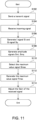
- FIG. 11 is a flowchart showing an example of an operation procedure in which a radar apparatus according to an embodiment of the present invention adjusts the gain of a received signal.
- the radar apparatus 300 first transmits a transmission signal whose frequency is changed over time (step S102).
- the radar apparatus 300 receives, as a reception signal, a radio wave returned from the transmission signal reflected by the object (step S104).
- the radar apparatus 300 generates I signals Si and Q signals Sq in the baseband band based on the received reception signal (step S 106).
- the radar apparatus 300 generates amplitude signals Smi indicating the amplitude of I signals Si in the baseband band and Smq indicating the amplitude of Q signals Sq in the baseband band (step S108).
- the radar apparatus 300 selects the higher level of the amplitude signal Smi and the amplitude signal Smq as the maximum value signal Smax (step S 110).
- the radar apparatus 300 generates the maximum value signal Fmax by filtering the maximum value signal Smax (step S112).
- the radar apparatus 300 adjusts the gain of the received signal based on the maximum value signal Fmax. More specifically, the gain adjusting module 40 in the radar apparatus 300 outputs a control voltage corresponding to the level of the maximum value signal Fmax to the variable gain amplifier in the reception module 150 (step S114).
- the transmission module 120 transmits a transmission signal whose frequency is changed with time.
- the reception module 150 receives, as a reception signal, a radio wave returned from a transmission signal reflected by an object.
- the frequency conversion module 170 generates an I signal Si and a Q signal Sq based on the reception signal.
- the amplitude signal generator 10 generates an amplitude signal Smi indicating the amplitude of the I signal Si and an amplitude signal Smq indicating the amplitude of the Q signal Sq.
- the maximum value selector 20 selects the higher level of the amplitude signal Smi and the amplitude signal Smq as the maximum value signal Smax.
- the gain adjustment module 40 adjusts the gain of the received signal based on the maximum value signal Smax.
- the process of generating the amplitude signal Smi and the amplitude signal Smq and selecting the maximum value signal Smax can be realized by a simple circuit configuration consisting of general-purpose components such as an operational amplifier, a resistor, a capacitor, and a diode.
Landscapes
- Engineering & Computer Science (AREA)
- Computer Networks & Wireless Communication (AREA)
- Physics & Mathematics (AREA)
- General Physics & Mathematics (AREA)
- Radar, Positioning & Navigation (AREA)
- Remote Sensing (AREA)
- Radar Systems Or Details Thereof (AREA)
Applications Claiming Priority (2)
| Application Number | Priority Date | Filing Date | Title |
|---|---|---|---|
| JP2021135427 | 2021-08-23 | ||
| PCT/JP2022/012633 WO2023026548A1 (ja) | 2021-08-23 | 2022-03-18 | レーダ装置および利得調整方法 |
Publications (2)
| Publication Number | Publication Date |
|---|---|
| EP4394433A1 true EP4394433A1 (de) | 2024-07-03 |
| EP4394433A4 EP4394433A4 (de) | 2025-09-03 |
Family
ID=85322670
Family Applications (1)
| Application Number | Title | Priority Date | Filing Date |
|---|---|---|---|
| EP22860846.9A Pending EP4394433A4 (de) | 2021-08-23 | 2022-03-18 | Radarvorrichtung und verstärkungseinstellungsverfahren |
Country Status (4)
| Country | Link |
|---|---|
| US (1) | US20240201325A1 (de) |
| EP (1) | EP4394433A4 (de) |
| JP (1) | JPWO2023026548A1 (de) |
| WO (1) | WO2023026548A1 (de) |
Family Cites Families (13)
| Publication number | Priority date | Publication date | Assignee | Title |
|---|---|---|---|---|
| US5315303A (en) * | 1991-09-30 | 1994-05-24 | Trw Inc. | Compact, flexible and integrated millimeter wave radar sensor |
| JPH0832383A (ja) * | 1994-07-14 | 1996-02-02 | Matsushita Electric Ind Co Ltd | 自動利得制御装置 |
| JPH08316997A (ja) * | 1995-05-15 | 1996-11-29 | Matsushita Electric Ind Co Ltd | 受信装置 |
| JP2001228240A (ja) | 2000-02-18 | 2001-08-24 | Matsushita Electric Ind Co Ltd | Fmcwレーダの受信信号増幅装置 |
| JP2007170819A (ja) * | 2005-12-19 | 2007-07-05 | Tdk Corp | パルス波レーダー装置 |
| JP4765915B2 (ja) * | 2006-12-01 | 2011-09-07 | 三菱電機株式会社 | Fm−cwレーダ装置 |
| WO2011074164A1 (ja) * | 2009-12-15 | 2011-06-23 | パナソニック株式会社 | 自動利得制御装置、受信機、電子機器、及び自動利得制御方法 |
| JP5810287B2 (ja) * | 2010-07-29 | 2015-11-11 | パナソニックIpマネジメント株式会社 | レーダ装置 |
| US9285461B2 (en) * | 2013-03-12 | 2016-03-15 | Nokia Technologies Oy | Steerable transmit, steerable receive frequency modulated continuous wave radar transceiver |
| KR20150102854A (ko) * | 2014-02-28 | 2015-09-08 | 한국과학기술원 | 주파수 변조 및 연속파를 이용한 큐밴드 장거리 레이더 시스템 및 방법 |
| JP2018025475A (ja) * | 2016-08-10 | 2018-02-15 | 株式会社デンソー | レーダ用送受信機 |
| US9831836B1 (en) * | 2016-10-07 | 2017-11-28 | Silicon Laboratories Inc. | Automatic gain control (AGC) circuit and method to control amplifier gain based on a duration of an overload condition |
| JP2021092585A (ja) * | 2021-02-26 | 2021-06-17 | 住友電気工業株式会社 | 電波センサおよび検知プログラム |
-
2022
- 2022-03-18 JP JP2023543665A patent/JPWO2023026548A1/ja active Pending
- 2022-03-18 WO PCT/JP2022/012633 patent/WO2023026548A1/ja not_active Ceased
- 2022-03-18 EP EP22860846.9A patent/EP4394433A4/de active Pending
-
2024
- 2024-03-01 US US18/592,635 patent/US20240201325A1/en active Pending
Also Published As
| Publication number | Publication date |
|---|---|
| US20240201325A1 (en) | 2024-06-20 |
| EP4394433A4 (de) | 2025-09-03 |
| JPWO2023026548A1 (de) | 2023-03-02 |
| WO2023026548A1 (ja) | 2023-03-02 |
Similar Documents
| Publication | Publication Date | Title |
|---|---|---|
| US4085368A (en) | Interference canceling method and apparatus | |
| US4731796A (en) | Multi-mode radio transceiver | |
| US5563550A (en) | Recovery of data from amplitude modulated signals with self-coherent demodulation | |
| US5497160A (en) | Method and apparatus for improved auto-correlation and range correlation in pseudo-random noise coded systems | |
| KR20010014248A (ko) | 송신장치 | |
| US10921434B2 (en) | Radar system | |
| AU4766093A (en) | Apparatus for compensating of phase rotation in a final amplifier stage | |
| US9197175B2 (en) | Methods and systems for pre-emphasis of an envelope tracking power amplifier supply voltage | |
| US11012162B2 (en) | Local oscillator leakage detecting and cancellation | |
| CN108169736A (zh) | 雷达系统中的同相(i)和正交(q)不平衡估计 | |
| CN113534145A (zh) | 一种基于线性调频连续波体制的高度表测高方法及系统 | |
| CN111190144A (zh) | 雷达装置及其泄漏修正方法 | |
| US4211979A (en) | Circuit arrangement for eliminating waveform distortion of an angle-modulated signal transmitted over multipaths | |
| CN109061580A (zh) | 一种调频间断连续波雷达缓和相互干扰方法 | |
| EP4394433A1 (de) | Radarvorrichtung und verstärkungseinstellungsverfahren | |
| EP0117946B1 (de) | System zur Messung der Interferenz von benachbarten Kanälen | |
| CN112034429A (zh) | 一种消除干扰自激的自适应数字对消方法 | |
| US7224717B1 (en) | System and method for cross correlation receiver | |
| GB2545028A (en) | Receiver with automatic gain control by an alternating current closed loop | |
| US5594760A (en) | Automatic gain control circuit and apparatus including such a circuit | |
| CN113346960A (zh) | 一种用于太赫兹空间正交调制信号合成校准的方法及系统 | |
| EP0991236A2 (de) | Vorrichtung und Verfahren zur Schätzung der Zentralfrequenz eines Empfangssignals | |
| Kurniawan et al. | Implementation of automatic I/Q imbalance correction for FMCW radar system | |
| JP7433528B2 (ja) | レーダ装置および干渉波抑圧装置 | |
| US5646627A (en) | Method and apparatus for controlling a biphase modulation to improve autocorrelation in pseudorandom noise coded systems |
Legal Events
| Date | Code | Title | Description |
|---|---|---|---|
| STAA | Information on the status of an ep patent application or granted ep patent |
Free format text: STATUS: THE INTERNATIONAL PUBLICATION HAS BEEN MADE |
|
| PUAI | Public reference made under article 153(3) epc to a published international application that has entered the european phase |
Free format text: ORIGINAL CODE: 0009012 |
|
| STAA | Information on the status of an ep patent application or granted ep patent |
Free format text: STATUS: REQUEST FOR EXAMINATION WAS MADE |
|
| 17P | Request for examination filed |
Effective date: 20240311 |
|
| AK | Designated contracting states |
Kind code of ref document: A1 Designated state(s): AL AT BE BG CH CY CZ DE DK EE ES FI FR GB GR HR HU IE IS IT LI LT LU LV MC MK MT NL NO PL PT RO RS SE SI SK SM TR |
|
| DAV | Request for validation of the european patent (deleted) | ||
| DAX | Request for extension of the european patent (deleted) | ||
| A4 | Supplementary search report drawn up and despatched |
Effective date: 20250730 |
|
| RIC1 | Information provided on ipc code assigned before grant |
Ipc: G01S 7/285 20060101AFI20250725BHEP Ipc: G01S 13/34 20060101ALI20250725BHEP Ipc: G01S 7/03 20060101ALI20250725BHEP Ipc: G01S 7/35 20060101ALI20250725BHEP Ipc: G01S 7/40 20060101ALI20250725BHEP |