EP4386850B1 - Bilderfassungsvorrichtung - Google Patents
Bilderfassungsvorrichtung Download PDFInfo
- Publication number
- EP4386850B1 EP4386850B1 EP23215797.4A EP23215797A EP4386850B1 EP 4386850 B1 EP4386850 B1 EP 4386850B1 EP 23215797 A EP23215797 A EP 23215797A EP 4386850 B1 EP4386850 B1 EP 4386850B1
- Authority
- EP
- European Patent Office
- Prior art keywords
- layer
- openings
- doping
- vias
- forming
- Prior art date
- Legal status (The legal status is an assumption and is not a legal conclusion. Google has not performed a legal analysis and makes no representation as to the accuracy of the status listed.)
- Active
Links
Images


Classifications
-
- H—ELECTRICITY
- H10—SEMICONDUCTOR DEVICES; ELECTRIC SOLID-STATE DEVICES NOT OTHERWISE PROVIDED FOR
- H10F—INORGANIC SEMICONDUCTOR DEVICES SENSITIVE TO INFRARED RADIATION, LIGHT, ELECTROMAGNETIC RADIATION OF SHORTER WAVELENGTH OR CORPUSCULAR RADIATION
- H10F39/00—Integrated devices, or assemblies of multiple devices, comprising at least one element covered by group H10F30/00, e.g. radiation detectors comprising photodiode arrays
- H10F39/80—Constructional details of image sensors
- H10F39/811—Interconnections
-
- H—ELECTRICITY
- H10—SEMICONDUCTOR DEVICES; ELECTRIC SOLID-STATE DEVICES NOT OTHERWISE PROVIDED FOR
- H10F—INORGANIC SEMICONDUCTOR DEVICES SENSITIVE TO INFRARED RADIATION, LIGHT, ELECTROMAGNETIC RADIATION OF SHORTER WAVELENGTH OR CORPUSCULAR RADIATION
- H10F39/00—Integrated devices, or assemblies of multiple devices, comprising at least one element covered by group H10F30/00, e.g. radiation detectors comprising photodiode arrays
- H10F39/011—Manufacture or treatment of image sensors covered by group H10F39/12
-
- H—ELECTRICITY
- H10—SEMICONDUCTOR DEVICES; ELECTRIC SOLID-STATE DEVICES NOT OTHERWISE PROVIDED FOR
- H10F—INORGANIC SEMICONDUCTOR DEVICES SENSITIVE TO INFRARED RADIATION, LIGHT, ELECTROMAGNETIC RADIATION OF SHORTER WAVELENGTH OR CORPUSCULAR RADIATION
- H10F39/00—Integrated devices, or assemblies of multiple devices, comprising at least one element covered by group H10F30/00, e.g. radiation detectors comprising photodiode arrays
- H10F39/011—Manufacture or treatment of image sensors covered by group H10F39/12
- H10F39/018—Manufacture or treatment of image sensors covered by group H10F39/12 of hybrid image sensors
-
- H—ELECTRICITY
- H10—SEMICONDUCTOR DEVICES; ELECTRIC SOLID-STATE DEVICES NOT OTHERWISE PROVIDED FOR
- H10F—INORGANIC SEMICONDUCTOR DEVICES SENSITIVE TO INFRARED RADIATION, LIGHT, ELECTROMAGNETIC RADIATION OF SHORTER WAVELENGTH OR CORPUSCULAR RADIATION
- H10F39/00—Integrated devices, or assemblies of multiple devices, comprising at least one element covered by group H10F30/00, e.g. radiation detectors comprising photodiode arrays
- H10F39/011—Manufacture or treatment of image sensors covered by group H10F39/12
- H10F39/026—Wafer-level processing
-
- H—ELECTRICITY
- H10—SEMICONDUCTOR DEVICES; ELECTRIC SOLID-STATE DEVICES NOT OTHERWISE PROVIDED FOR
- H10F—INORGANIC SEMICONDUCTOR DEVICES SENSITIVE TO INFRARED RADIATION, LIGHT, ELECTROMAGNETIC RADIATION OF SHORTER WAVELENGTH OR CORPUSCULAR RADIATION
- H10F39/00—Integrated devices, or assemblies of multiple devices, comprising at least one element covered by group H10F30/00, e.g. radiation detectors comprising photodiode arrays
- H10F39/80—Constructional details of image sensors
- H10F39/809—Constructional details of image sensors of hybrid image sensors
Definitions
- This description relates generally to the field of electronic devices and more particularly to the field of image acquisition devices, and in particular to devices comprising a stack of an infrared image sensor and a visible image sensor.
- An image acquisition device comprising a stack of several sensors and in particular sensors of different types, for example an infrared image sensor and a visible image sensor, for example with a view to simultaneously or successively acquiring a visible image and depth map of the same scene.
- said conductive vias have a doping gradient decreasing from the upper face of the substrate.
- the conductive vias are doped with phosphorus or arsenic atoms.
- said vias have a doping gradient decreasing from the upper face of the substrate.
- said film has a doping of the order of 1.10 21 at/cm 3 .
- the amorphous silicon of the film is further doped in situ during its deposition.
- the silicon of said layer is doped in situ during its deposition.
- said layer has a doping, in the vicinity of the substrate, of the order of 1.10 21 at/cm 3 .
- the method comprises, after the formation of the openings in the insulating layer in contact with the photo-detection pixels, a step of amorphizing the surface of the substrate and the surface of polycrystalline silicon conductive grids at the bottom of the openings.
- Another embodiment provides an image acquisition device comprising a first image sensor and a second image sensor as defined above, the first image sensor and the second image sensor being stacked.
- the expressions "about”, “approximately”, “substantially”, and “of the order of” mean to within 10%, preferably to within 5%.
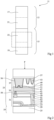
- FIG. 1 is a partial and schematic sectional view of an image acquisition device 11 according to one embodiment.
- the image acquisition device 11 corresponds, for example, to the assembly of a first structure 13 corresponding to a first image sensor, and a second structure 15 corresponding to a second image sensor.
- the first image sensor is, for example, an infrared image sensor and the second image sensor is, for example, a visible image sensor, for example a color image sensor.
- the two infrared 13 and visible 15 sensors are stacked one on top of the other.
- each of the sensors 13 and 15 comprises a set of pixels formed in and on a semiconductor substrate.
- Each pixel comprises, for example, a photoreceptor, for example a photodiode, and a reading circuit for the photoreceptor.
- the sensor 13 comprises a set of pixels 17 and the sensor 15 comprises a set of pixels 19.
- each of the sensors 13 and 15 comprises an interconnection network for the pixels of the sensor.
- the sensor 13 thus comprises an interconnection network 21 and the sensor 15 comprises an interconnection network 23.
- the infrared sensor 13 is arranged on the visible sensor 15.
- the lower face of the interconnection network 21 of the sensor 13 is in contact with the upper face of the interconnection network 23 of the sensor 15.
- the set of pixels 17 of the infrared sensor 13 is arranged on the side of the upper face of the interconnection network 21.
- the set of pixels 19 of the visible sensor 15 is arranged on the side of the lower face of the interconnection network 23.
- the device 11 is, in the example illustrated in Figure 1 , intended to be illuminated from its lower face.
- the visible radiation is absorbed by the photodetectors of the pixels of the sensor 15, which allows the acquisition of an image in the range of wavelengths of the visible spectrum.
- the sensor 15 is, on the other hand, substantially transparent to infrared radiation. These rays are absorbed by the photodetectors of the sensor 13, which allows the acquisition of an image in the wavelength range of the infrared and near-infrared spectrum.
- the sensor pixels are for example arranged in a matrix according to rows and columns.
- FIG. 2 is a more detailed sectional view of part of the image acquisition device 11 of the Figure 1 . More precisely, the Figure 2 represents in more detail the part of the device 11 of the Figure 1 surrounded by dotted lines in Figure 1 , that is to say a part of the interconnection network 23 and a part of the set of pixels 19 of the sensor 15.
- each pixel P comprises a photodetector, not shown, formed in and on a substrate 25.
- the substrate 25 is for example made of a semiconductor material, for example silicon.
- Each photodetector is for example connected to a reading circuit comprising transistors comprising gates 27, formed on the substrate 25.
- the gates 27 are, for example, made of polycrystalline silicon, for example doped with a first conductivity type, for example N type, for example doped with phosphorus atoms.
- the layer 29 is made of a nitride and/or an oxide, for example a silicon nitride (Si x N y ), a silicon carbonitride (SiC x N y ) and/or a silicon dioxide (SiO 2 ).
- the layer 29 comprises a first sub-layer on and in contact with the upper face of the substrate 25 and the upper face of the gates 27 and a second sub-layer on and in contact with the upper face of the first sub-layer.
- the first sub-layer is for example made of silicon dioxide.
- the second sub-layer is for example made of silicon nitride.
- the interconnection network 23 consists of a stack or network of electrically conductive levels and electrically insulating levels in which interconnection elements are formed.
- Figure 2 three levels are represented in the interconnection network 23, a first level 31 called the lower level, covering the upper face of the substrate 25, for example on and in contact with the upper face of the layer 29, a second level 33 covering the first level, for example on and in contact with the upper face of the first level, and a third level covering the second level, for example on and in contact with the upper face of the second level.
- the network 23 may comprise a number of levels other than three, for example greater than three.
- each level includes a layer of insulating material in which conductive tracks and vias are formed.
- the lower level 31 thus comprises, for example, an electrically insulating layer 37 in which electrically conductive vias 39 and electrically conductive tracks 41 are formed.
- the second level 33 comprises, for example, an electrically insulating layer 43 in which electrically conductive vias 45 and electrically conductive tracks 47 are formed and the third level 35 comprises, for example, an electrically insulating layer 49 in which electrically conductive vias 45 and electrically conductive tracks 47 are formed. electrically conductive tracks 51 and electrically conductive tracks 53.
- the vias 39 are in contact, by their lower face, with the substrate 25 or with the gates 27 of the transistors of the pixel reading circuits, and, by their upper face, with the lower face of the tracks 41.
- the vias 45 are for example in contact, by their lower face, with the upper face of the tracks 41, and, by their upper face, with the lower face of the tracks 47.
- the vias 51 are for example in contact, by their lower face, with the upper face of the tracks 47, and, by their upper face, with the lower face of the tracks 53.
- the layers 37, 43 and 49 are for example made of silicon dioxide (SiO 2 ) and/or silicon nitride (Si x N y ) and/or silicon carbonitride (SiC x N y ).
- the layers 37, 43 and 49 each correspond to a stack of the aforementioned materials.
- Vias 45 and 51 and tracks 47 and 53 are for example made of metal, for example a transition metal, for example tungsten, copper, cobalt or ruthenium.
- metal for example a transition metal, for example tungsten, copper, cobalt or ruthenium.
- vias 45 are made of tungsten
- vias 51 and tracks 53 and 47 are made of copper.
- the levels of the interconnection network 23 are separated by encapsulation layers.
- an encapsulation layer 55 thus covers the second level and an encapsulation layer 57 covers the third level of the interconnection network 23.
- the encapsulation layers 55 and 57 are, for example, made of an electrically insulating material making it possible to act as a barrier to the diffusion of copper or certain ions in the silicon of the layers 37, 43 and 49.
- the encapsulation layers 55 and 57 are made of a material other than copper, for example silicon nitride or silicon carbonitride (SiCN).
- the vias 45 and 51 and tracks 53 and 47 are for example surrounded by a layer making it possible to act as a barrier to the diffusion of the material of the vias, for example copper or tungsten, in the silicon of the layers 43 and 49.
- the vias 51 and the tracks 53 and 47 are for example surrounded, for example encapsulated, by a barrier layer 56 and the via 45 is for example surrounded by a barrier layer 58.
- the barrier layer 56 is for example made of tantalum nitride (TaN) and the barrier layer 58 is for example made of titanium and/or titanium nitride (TiN).
- the conductive tracks 41 of the level 31 are arranged on and in contact with a layer 63 and are covered and in contact with a layer 59.
- the layers 63 and 59 are for example both made of a dielectric material, for example nitride, for example silicon nitride.
- the transparency of the sensor 15, to the radiation captured by the sensor 13, is provided by the transparency of all the elements described above and more particularly of all the photodetectors 19 and the interconnection network 23.
- the set of pixels 19 of the sensor 15 is transparent to infrared radiation.
- the interconnection network 23 may, however, comprise electrical connection elements (electrical connection tracks and/or vias), for example metallic, which are not transparent to infrared radiation.
- the vias 39 of the lower level 31 of the interconnection network 23 allow contact to be reestablished on the upper face of the gates 27 as well as at different locations on the surface of the substrate 25, for example on reading nodes of the P pixels. Their deportation to the periphery of the P pixels is therefore not possible.
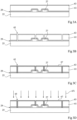
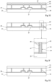
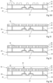
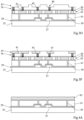
- FIGS. 3A , there Figure 3B , there Figure 3C , there 3D figure , there Figure 3E , there Figure 3F , there Figure 3G , there Figure 3H , there Figure 3I , there Figure 3J , there Figure 3K , there Figure 3L , there figure 3M , there Figure 3N , there Figure 3O and the Figure 3P are sectional views illustrating steps of a method of manufacturing the part of the image acquisition device illustrated in Figure 2 according to a first mode of implementation.
- FIG. 3A illustrates a starting structure of the process. More specifically, the Figure 3A illustrates in a way very schematic only part of the elements of a pixel P.
- the structure illustrated in Figure 3A comprises the substrate 25 in and on which the plurality of photodetectors and readout transistors are formed.
- the structure illustrated in Figure 3A includes the gates 27 of read transistors formed on the substrate 25 and, for example, separated from the substrate 25 by a gate insulator layer (not detailed in the figure).
- the substrate 25 and the grids 27 are for example covered by the layer 29.
- the layer 29 is formed in a conformal manner, that is to say that it is deposited with a constant thickness over the entire surface of the structure.
- layer 29 is covered by an insulating layer 61.
- layer 61 is made of an oxide, for example silicon dioxide (SiO 2 ).
- layer 61 covers layer 29 with a thickness of between 190 nm and 500 nm, for example between 300 nm and 450 nm, for example of the order of 380 nm.
- the layer 61 is, for example, covered by a dielectric layer 63.
- the layer 63 is, for example, made of a nitride, for example silicon nitride (Si x N y ) or silicon carbonitride (SiC x N y ).
- the layer 63 has a thickness of between 10 nm and 100 nm, for example between 30 nm and 70 nm.
- FIG. 3B illustrates a structure obtained at the end of a step of forming openings 65 in the structure illustrated in Figure 3A .
- the openings 65 are formed from the upper face of the structure illustrated in Figure 3A , so that they open onto the upper face of the substrate 25 or the upper face of the grids 27.
- the openings 65 thus pass through the layer 63, the layer 61 and the layer 29.
- the openings 65 are, for example, formed by etching through a masking layer not shown.
- the openings 65 have a width between 50 nm and 150 nm, for example between 90 nm and 100 nm.
- FIG. 3C illustrates a structure obtained at the end of a step of depositing a silicon film 67 on the structure illustrated in Figure 3B . More particularly, the film 67 is deposited on the upper face of the layer 63 and in the openings 65, more particularly in the bottom and on the sides of the openings 65.
- the film 67 is, for example, made of amorphous silicon.
- the film 67 is, for example, deposited conformally, that is to say it is deposited over the entire upper face of the structure illustrated in Figure 3B with a substantially constant thickness.
- the film 67 has, for example, a thickness of between 19 nm and 40 nm, for example of between 30 nm and 35 nm.
- the film 67 is formed by low pressure chemical vapor deposition or LPCVD.
- the material constituting the film 67 is doped during its deposition on the upper face of the structure illustrated in Figure 3B , we speak of in-situ doping.
- the material constituting the film 67 is, for example, doped with a first type of conductivity, for example of the N type, for example doped with arsenic or phosphorus atoms.
- the film 67 has a doping of the order of 3.10 19 at/cm 3 .
- the deposition of the film 67 is preceded by a step of treating the surface of the structure illustrated in Figure 3C .
- FIG. 3D figure illustrates a structure obtained following a doping step of film 67 of the structure illustrated in Figure 3C .
- this step we come for example to dope the structure illustrated in Figure 3C by implantation of doping elements through its upper face, we speak here of ex-situ doping.
- this step is carried out without a mask or masking layer.
- the layer 63 can act as a masking layer by protecting the layer 61 from the implantation of dopants 67i.
- This doping step consists of the implantation in the film 67 of atoms of the first conductivity type, for example of the N type, for example of arsenic or phosphorus atoms.
- the doping is, for example, carried out with a dose of between 2.10 14 at/cm 2 and 1.10 16 at/cm 2 , for example of between 5.10 14 at/cm 2 and 1.10 16 at/cm 2 .
- the film 67 has a doping of between 4.10 19 at/cm 3 and 4.10 22 at/cm 3 , for example of the order of 1.10 21 at/cm 3 .
- FIG. 3E illustrates a structure obtained at the end of a step of filling the openings 65 of the structure illustrated in 3D figure .
- amorphous silicon used during this step is doped in situ during its deposition, for example of the first type of conductivity, for example of the N type, for example with arsenic or phosphorus atoms.
- the amorphous silicon used to form the layer 69 is for example doped in the order of 1.10 20 at/cm 3 .
- an additional doping step may be provided and more particularly a localized doping step of the second conductivity type, for example of the P type, for example doped with boron atoms or boron difluoride (BF 2 ).
- the purpose of this step is to locally dope the parts of the layer 69 located in a part of the openings 65 and more precisely the parts of the layer 69 located in the openings 65 which are in contact with a zone of the substrate 25 preferentially doped P.
- the localized doping is for example carried out through a masking layer, for example made of resin.
- FIG. 3F illustrates a structure obtained following a step of polishing the upper face of the structure illustrated in Figure 3E .
- an enlargement of a portion of the structure comprising a via 39 is also shown.
- the polishing step is, for example, carried out by a mechanical process, for example a chemical-mechanical process or CMP (from the English "Chemical Mechanical Polishing"). For example, this step makes it possible to flatten the upper face of the structure down to the layer 63 allowing the end of flattening to be checked.
- the material of the vias 39 changes from an amorphous state to a polycrystalline state.
- the vias 39 are, at the end of this step, made of doped polycrystalline silicon.
- the vias 39 being formed from the film 67 and the layer 69, their dopings are greater in the vicinity of the substrate 25, the vias 39 thus have a decreasing doping gradient starting from the upper face of the substrate 25.
- FIG. 3G illustrates a structure obtained at the end of a step of depositing a layer 73 on the upper face of the structure illustrated in Figure 3F .
- the layer 73 is more particularly deposited on and in contact with the upper face of the layer 63 and the upper face of the vias 39.
- the layer 73 is for example made of a dielectric material, for example silicon oxide, for example silicon dioxide (SiO 2 ).
- the layer 73 is deposited by plasma-enhanced chemical vapor deposition or PECVD (from the English "Plasma Enhanced Chemical Vapor Deposition").
- PECVD from the English "Plasma Enhanced Chemical Vapor Deposition”
- the layer 73 has a thickness between 100 nm and 500 nm, for example of the order of 155 nm.
- FIGH illustrates a structure obtained at the end of a step of forming openings 75 in the layer 73 of the structure illustrated in Figure 3G .
- This step is similar to the step of forming the openings 65 in the layers 61, 63 and 29 described in connection with the Figure 3B with the difference that the openings 75 are formed from the upper face of the layer 73 and that they open onto the upper face of the layer 63 and onto the upper face of the vias 39.
- the openings 75 are wider than the openings 65, the openings 65 accommodating the vias 39 and the openings 41 accommodating the first track level 41 of the interconnection network.
- each via 39 is surmounted by an opening 75.
- FIG. 3I illustrates a structure obtained at the end of a step of filling the openings 75 of the structure illustrated in Figure 3H .
- a second step the excess amorphous silicon deposited on the upper face of the structure is removed so as to reveal the upper face of the layer 73.
- this step is carried out by polishing.
- the polishing step is, for example, carried out by a mechanical process, for example a chemical-mechanical process or CMP (from the English "Chemical Mechanical Polishing").
- CMP from the English "Chemical Mechanical Polishing”
- the part of amorphous silicon remaining in the openings 75 thus forms the tracks 41.
- the face upper part of tracks 41 are flush with the upper face of layer 73.
- the polishing step is, for example, followed by an annealing step.
- the annealing step is carried out at a temperature above 800°C, for example above 900°C, for example between 900°C and 1050°C.
- the material of the tracks 41 passes from an amorphous state to a polycrystalline state.
- FIG. 3J illustrates a structure obtained at the end of a step of depositing a layer 59 on the upper face of the structure illustrated in Figure 3I .
- the upper face of layer 73 and the upper face of tracks 41 are more particularly covered with a layer 59.
- the layer 59 is, for example, formed as a full wafer.
- the layer 59 is formed conformally.
- the layer 41 has a thickness of between 10 nm and 100 nm, for example between 30 nm and 70 nm.
- the layer 41 is, for example, deposited by PECVD.
- the layer 59 is, for example, made of a dielectric material, for example a nitride, for example silicon nitride (Si x N y ) or silicon carbonitride (SiC x N y ).
- a dielectric material for example a nitride, for example silicon nitride (Si x N y ) or silicon carbonitride (SiC x N y ).
- step 59 completes the formation of the lower level 31 of the interconnection network 23.
- Steps 3K to 3O illustrate the formation of an additional level of the interconnection network 23, for example the second level 33, these steps are therefore, for example, repeated until the desired number of levels in the interconnection network 23 is obtained.
- FIG. 3K illustrates a structure obtained at the end of a step of forming a layer 79 on the face upper part of the structure illustrated in Figure 3J followed by a step of forming openings 81 in layers 79 and 59.
- the step of forming layer 79 is similar to the step of forming layer 79 described in connection with the Figure 3K and the step of forming the openings 81 is similar to the step of forming the openings 41 described in relation to the Figure 3H .
- the openings 81 are formed opposite the tracks 41 and open onto the tracks 41.
- FIG. 3L illustrates a structure obtained at the end of a step of cleaning the bottom of the openings 81 and forming a layer 82 on the upper face of the structure illustrated in Figure 3K .
- the bottom of the openings 81 is first cleaned, for example using an argon plasma.
- a full plate layer 82 is formed, comprising for example a sub-layer 82a and a sub-layer 82b, on the upper face of the structure illustrated in Figure 3K and more particularly on the upper face of layer 79 and on the sides and in the bottom of the openings 81.
- the sub-layer 82a is made of titanium.
- the sub-layer 82a has, for example, a thickness of less than 50 nm, for example less than 30 nm, for example between 5 nm and 30 nm.
- the sub-layer 82a is, for example, formed by a physical vapor deposition (PVD) process.
- the sub-layer 82b is, for example, formed on and in contact with the sub-layer 82a.
- the sub-layer 82b is made of silicon nitride.
- the sub-layer 82b is, for example, formed by the deposition of successive atomic layers (ALD). Layer Deposition").
- the underlayer 82b allows, for example, to protect the underlayer 82a from oxidation.
- FIG. 3M illustrates a structure obtained following an annealing step of the structure illustrated in Figure 3L so as to form an intermetallic silicide 83 from layer 82.
- the structure undergoes annealing to react the titanium of the sub-layer 82a with the silicon of the tracks 41 so as to form, in the bottom of the openings 81, a thin film of an intermetallic compound called silicide.
- the silicide is for example based on silicon and titanium, the silicide is a titanium disilicide (TiSi 2 ) or a titanium silicide (TiSi) depending on the annealing applied.
- FIG. 3N illustrates a structure obtained at the end of a step of filling the openings 81 of the structure illustrated in figure 3M , so as to form the vias 45.
- the metallic material is copper, tungsten or cobalt.
- the filling of the openings 81 is carried out while the parts of the layer 82 which have not reacted with the silicon of the contacts 41, during the step of forming the silicide 83, are kept on the sides of the openings 81.
- the layer 82 thus has a barrier function to the diffusion of the material of the vias 45 into the layer 79.
- a second step the excess metallic material deposited on the upper face of the structure is removed so as to reveal the upper face of layer 79.
- this step is carried out by polishing.
- the polishing step is, for example, carried out by a mechanical process, for example a chemical-mechanical process or CMP (from the English "Chemical Mechanical Polishing"). What remains of metallic material in the openings 81 thus forms the tracks 45.
- the upper face of the tracks 45 are flush with the upper face of the layer 79.
- FIG. 3O illustrates a structure obtained at the end of a step of forming a layer 87 on the upper face of the structure illustrated in Figure 3N followed by a step of forming openings 89 in layer 87.
- the step of forming layer 87 is similar to the step of forming layer 73 described in connection with the Figure 3G and the step of forming the openings 89 is similar to the step of forming the openings 41 described in connection with the Figure 3H .
- each via 45 is surmounted by an opening 89.
- FIG. 3P illustrates a structure obtained at the end of a step of filling the openings 89 of the structure illustrated in Figure 3O , so as to form tracks 47.
- the barrier layer is made of tantalum and/or tantalum nitride (TaN).
- the barrier layer comprises a first sub-layer made of tantalum nitride.
- the barrier layer comprises a second sub-layer made of tantalum.
- the contacts 47 are formed in the openings 89, on and in contact with the barrier layer.
- the contacts 47 are made of a metallic material, for example copper.
- the contacts 47 are formed by deposition of a layer of copper, for example full plate.
- the deposition of the copper layer is, for example, followed by electrolytic growth of this layer.
- a polishing step for example mechanochemical, is carried out so as to uncover the upper face of the layer 87.
- the upper face of the contacts 47 are flush with the upper face of the layer 87.
- level 33 of the interconnection network 23 is, for example, completed by the formation of a layer of a dielectric, for example of a nitride, for example of silicon nitride (Si x N y ) or silicon carbonitride (SiC x N y ).
- a layer of a dielectric for example of a nitride, for example of silicon nitride (Si x N y ) or silicon carbonitride (SiC x N y ).
- An advantage of the first embodiment is that it allows the doping of the part of the film 67 located on the sides of the openings 65, thus creating a more conductive zone on the side of the vias 39 and lowering the resistance of these.
- FIG. 4A and the Figure 4B are sectional views illustrating steps of a method of manufacturing the part of the image acquisition device illustrated in Figure 2 according to a second mode of implementation.
- the second embodiment differs from the first embodiment in that, upon completion of the step described in relation to the Figure 3B , the openings 65 are filled with a layer 93 of silicon without prior formation of the film 67 (as has been described in relation to the Figure 3C ) And in that layer 93 undergoes implantation following its deposition.
- FIG. 4A illustrates a structure obtained at the end of a step of depositing the layer 93 in the openings 65 and on the surface of the structure illustrated in Figure 3B .
- the layer is, during this step, doped in situ during its deposition, for example of the first type of conductivity, for example of the N type, for example with arsenic or phosphorus atoms.
- the amorphous silicon used to form the layer 93 is, for example, doped in the order of 1.10 19 at/cm 3 .
- FIG. 4B illustrates a structure obtained following a doping step of layer 93 of the structure illustrated in Figure 4A . During this step, we come for example to dope the structure illustrated in Figure 4A by its upper face.
- this step is performed without a mask or masking layer.
- layer 63 can act as a masking layer by protecting layer 61 from the implantation of 93i dopants.
- this doping step consists of the implantation in the aforementioned layer of arsenic or phosphorus atoms.
- the doping of layer 93 corresponds to deep doping, that is to say that the parts of layer 93 located at the bottom of openings 65 will be more doped than the parts of layer 93 located on the surface of the openings 65.
- Doping is, for example, carried out with a dose between 2.10 14 at/cm 2 and 1.10 16 at/cm 2 , for example between 5.10 14 at/cm 2 and 1.10 16 at/cm 2 .
- the layer 93 has, for example, a doping, in the vicinity of the substrate 25 and the grids 27, of between 4.10 19 at/cm 3 and 4.10 22 at/cm 3 , for example of the order of 1.10 21 at/cm 3 .
- an additional doping step can be provided and more particularly a localized doping step of the second type of conductivity, for example of the P type similarly to what has been described in relation to the Figure 3E .
- the second embodiment is identical to the first embodiment, the doping step is then followed by the steps illustrated in Figures 3F to 3O .
- the step described in relation to the Figure 3F polishing and annealing of the structure makes it possible to form the vias 39 from the layer 93.
- the material of the vias 39 changes from an amorphous state to a polycrystalline state.
- the vias 39 are, at the end of this step, made of doped polycrystalline silicon with a decreasing doping gradient starting from the upper face of the substrate 25.
- FIG. 5 is a sectional view illustrating a step in a method of manufacturing the portion of the image acquisition device illustrated in Figure 2 according to a third mode of implementation.
- the third embodiment is similar to the first embodiment except that it includes a step of treating the upper face of the structure illustrated in Figure 3B .
- this step for example, we amorphize the upper face of the structure illustrated in Figure 3B and more particularly, the parts of the surface of the grids 27 and of the substrate 25 located opposite the openings 65.
- This step allows a crystallographic rearrangement of the parts mentioned above and thus a better electrical contact with the via 39 formed subsequently in the openings 65.
- this step consists of the implantation of neutral ions 27i, for example argon, nitrogen, fluorine, silicon or germanium.
- neutral ions 27i for example argon, nitrogen, fluorine, silicon or germanium.
- the third embodiment is identical to the first embodiment.
- the step illustrated in Figure 5 is followed by a step of forming polycrystalline silicon contacts not having a doping gradient.
- the ohmic contact between the vias 39 and the substrate 25 or the gates 27 remains improved due to the crystallographic rearrangement resulting from the step of surface amorphization of the silicon at the bottom of the openings 65.
- An advantage of the described embodiments is that they allow polycrystalline silicon vias 39 to be formed in a lower level of the interconnection network with a doping gradient, thereby improving ohmic contact with the gates 27 or the substrate 25.
- the second and third embodiments may be combined.
- the described embodiments can be applied in the context of a device comprising a single sensor illuminated by its upper face.
- the interconnection network is then made transparent to the radiation captured by the detectors of the same sensor.
Landscapes
- Solid State Image Pick-Up Elements (AREA)
Claims (15)
- Bildsensor (15), aufweisend:- eine Vielzahl von Fotodetektionspixeln (19), die innerhalb und auf einem Halbleitersubstrat (25) ausgebildet sind; und- ein Verbindungsnetzwerk (23), das eine Oberfläche des Halbleitersubstrats bedeckt, wobei das Verbindungsnetzwerk eine Ebene (31) leitender Durchkontaktierungen (39) aufweist, die mit ihrer unteren Oberfläche mit den Fotodetektionspixeln in Kontakt stehen,wobei die leitenden Durchkontaktierungen aus dotiertem Polysilizium bestehen und dadurch gekennzeichnet sind, dass die Durchkontaktierungen auf ihrer unteren Oberflächenseite eine stärkere Dotierung aufweisen als auf ihrer oberen Oberflächenseite.
- Sensor nach Anspruch 1, wobei die leitenden Durchkontaktierungen (39) einen abnehmenden Dotierungsgradienten aufweisen, der von der oberen Oberfläche des Substrats (25) ausgeht.
- Bildsensor nach Anspruch 1 oder 2, wobei die leitenden Durchkontaktierungen (39) mit Phosphor- oder Arsenatomen dotiert sind.
- Verfahren zur Herstellung eines Bildsensors (15), aufweisend:- das Ausbilden einer Vielzahl von Fotodetektionspixeln (19) innerhalb und auf einem Halbleitersubstrat (25); und- das Ausbilden einer Ebene (31) von leitenden Durchkontaktierungen (39) eines Verbindungsnetzwerks (23), wobei die Durchkontaktierungen (39) mit ihrer unteren Oberfläche mit den Fotodetektionspixeln in Kontakt stehen, wobei die leitenden Durchkontaktierungen (39) aus dotiertem Polysilizium bestehen und auf ihrer unteren Oberflächenseite eine stärkere Dotierung aufweisen als auf ihrer oberen Oberflächenseite.
- Verfahren nach Anspruch 4, wobei die Durchkontaktierungen (39) einen abnehmenden Dotierungsgradienten aufweisen, der von der oberen Oberfläche des Substrats ausgeht.
- Verfahren nach Anspruch 4 oder 5, wobei das Ausbilden der leitenden Durchkontaktierungen (39) einen Schritt des Ausbildens von Öffnungen (65) in einer Isolierschicht (61) in Kontakt mit den Fotodetektionspixeln (19) aufweist.
- Verfahren nach Anspruch 6, wobei das Ausbilden der leitenden Durchkontaktierungen (39) nach dem Schritt des Ausbildens der Öffnungen (65) die folgenden aufeinanderfolgenden Schritte aufweist:- Ausbilden eines amorphen Siliziumfilms (67) auf und im Inneren der Öffnungen (65);- Ex-situ-Dotieren des Films (67) durch Implantation von Dotierstoffen; und- Füllen der Öffnungen (65) mit einer amorphen Siliziumschicht (69).
- Verfahren nach Anspruch 7, wobei der Film am Ende des Schritts der Dotierung des Films (67) eine Dotierung in der Größenordnung von 1,1021 at/cm3 aufweist.
- Verfahren nach Anspruch 7 oder 8, wobei das amorphe Silizium des Films (67) ferner während seiner Abscheidung in-situ dotiert wird.
- Verfahren nach einem der Ansprüche 7 bis 9, wobei das Silizium der Schicht (69) während seiner Abscheidung in-situ dotiert wird.
- Verfahren nach Anspruch 6, wobei das Ausbilden der leitenden Durchkontaktierungen (39) nach dem Schritt des Ausbildens der Öffnungen (65) die folgenden aufeinanderfolgenden Schritte aufweist:- Füllen der Öffnungen (65) mit einer amorphen Siliziumschicht (93); und- Ex-situ-Dotieren der Schicht (93) in der Nähe des Halbleitersubstrats (25) durch Implantation von Dotierstoffen.
- Verfahren nach Anspruch 11, wobei das Silizium der Schicht (93) während seiner Abscheidung ferner in-situ dotiert wird.
- Verfahren nach Anspruch 11 oder 12, wobei die Schicht am Ende des Schritts des Dotierens der Schicht (93) in der Nähe des Substrats (25) eine Dotierung in der Größenordnung von 1,1021 at/cm3 aufweist.
- Verfahren nach einem der Ansprüche 6 bis 13, dass nach dem Ausbilden der Öffnungen (65) in der Isolierschicht (61) in Kontakt mit den Fotodetektionspixeln einen Schritt der Amorphisierung der Oberfläche des Substrats (25) und der Oberfläche von leitenden Polysilizium-Gates (27) am Boden der Öffnungen (65) aufweist.
- Bildaufnahmevorrichtung (11), die einen ersten Bildsensor (13) und einen zweiten Bildsensor (15) aufweist, gemäß einem der Ansprüche 1 bis 3, wobei der erste Bildsensor und der zweite Bildsensor gestapelt sind.
Applications Claiming Priority (1)
| Application Number | Priority Date | Filing Date | Title |
|---|---|---|---|
| FR2213292A FR3143852B1 (fr) | 2022-12-14 | 2022-12-14 | Dispositif d'acquisition d'images |
Publications (2)
| Publication Number | Publication Date |
|---|---|
| EP4386850A1 EP4386850A1 (de) | 2024-06-19 |
| EP4386850B1 true EP4386850B1 (de) | 2025-04-23 |
Family
ID=85727122
Family Applications (1)
| Application Number | Title | Priority Date | Filing Date |
|---|---|---|---|
| EP23215797.4A Active EP4386850B1 (de) | 2022-12-14 | 2023-12-12 | Bilderfassungsvorrichtung |
Country Status (3)
| Country | Link |
|---|---|
| US (1) | US20240204029A1 (de) |
| EP (1) | EP4386850B1 (de) |
| FR (1) | FR3143852B1 (de) |
Family Cites Families (6)
| Publication number | Priority date | Publication date | Assignee | Title |
|---|---|---|---|---|
| TW200644165A (en) * | 2005-05-04 | 2006-12-16 | Icemos Technology Corp | Silicon wafer having through-wafer vias |
| US20080099924A1 (en) * | 2005-05-04 | 2008-05-01 | Icemos Technology Corporation | Silicon Wafer Having Through-Wafer Vias With A Predetermined Geometric Shape |
| FR2949173A1 (fr) * | 2009-08-12 | 2011-02-18 | St Microelectronics Sa | Capteur d'images eclaire par la face arriere protege des rayons infrarouges |
| FR2954587B1 (fr) * | 2009-11-10 | 2012-07-20 | St Microelectronics Sa | Procede de formation d'un capteur d'images eclaire par la face arriere |
| CN104795418B (zh) * | 2015-04-24 | 2018-09-18 | 上海珏芯光电科技有限公司 | 感光成像装置及其制造方法 |
| CN110880520B (zh) * | 2018-09-06 | 2024-11-29 | 松下知识产权经营株式会社 | 摄像装置 |
-
2022
- 2022-12-14 FR FR2213292A patent/FR3143852B1/fr active Active
-
2023
- 2023-12-12 EP EP23215797.4A patent/EP4386850B1/de active Active
- 2023-12-12 US US18/536,511 patent/US20240204029A1/en active Pending
Also Published As
| Publication number | Publication date |
|---|---|
| FR3143852A1 (fr) | 2024-06-21 |
| FR3143852B1 (fr) | 2024-12-20 |
| US20240204029A1 (en) | 2024-06-20 |
| EP4386850A1 (de) | 2024-06-19 |
Similar Documents
| Publication | Publication Date | Title |
|---|---|---|
| EP1365444B1 (de) | Grabenkondensator mit zwei vom Substrat unabhängigen Elektroden | |
| FR2930840A1 (fr) | Procede de reprise de contact sur un circuit eclaire par la face arriere | |
| FR2782415A1 (fr) | Dipositif de memoire a semiconducteur haute densite et son procede de fabrication | |
| FR3098988A1 (fr) | Capteur d'image | |
| TW200950067A (en) | Backside illuminated image sensor having deep light reflective trenches | |
| FR2954587A1 (fr) | Procede de formation d'un capteur d'images eclaire par la face arriere | |
| FR2563048A1 (fr) | Procede de realisation de contacts d'aluminium a travers une couche isolante epaisse dans un circuit integre | |
| FR3030113A1 (fr) | Capteur d'image eclaire et connecte par sa face arriere | |
| FR3100926A1 (fr) | Capteur d'images réalisé en technologie 3D séquentielle | |
| FR2845522A1 (fr) | Circuit integre a couche enterree fortement conductrice | |
| EP0461967A2 (de) | Halbleiteranordnung mit Schottky-Übergang für Mikrowellenverstärkung und schnelle logische Schaltungen und Verfahren zu deren Herstellung | |
| EP3098851A2 (de) | Herstellungsverfahren eines infrarot-filters in verbindung mit einem bildsensor | |
| CN113629088A (zh) | 金属栅格的制造方法、背照式图像传感器及其制造方法 | |
| FR2694134A1 (fr) | Procédé de fabrication d'une diode photovoltaïque et diode à structure plane. | |
| EP4386850A1 (de) | Bilderfassungsvorrichtung | |
| FR3000840A1 (fr) | Procede de realisation de contacts metalliques au sein d'un circuit integre, et circuit integre correspondant | |
| WO2003026016A2 (fr) | Capteur d'image avec creusement des couches de planarisation et procede de fabrication | |
| FR2962595A1 (fr) | Dispositif microélectronique a niveaux métalliques d'interconnexion connectes par des vias programmables | |
| FR3057395A1 (fr) | Capteur d'image a eclairement par la face arriere | |
| US8421228B2 (en) | Structure and methods of forming contact structures | |
| EP1774588A1 (de) | Zusammenfügen zweier substrate mittels molekularer adhäsion | |
| FR3083001A1 (fr) | Capteur d'images | |
| FR3108786A1 (fr) | Pixel d'un capteur de lumière et son procédé de fabrication | |
| FR2894069A1 (fr) | Fabrication de transistors mos | |
| EP4125141A1 (de) | Phasenwechselspeicher |
Legal Events
| Date | Code | Title | Description |
|---|---|---|---|
| PUAI | Public reference made under article 153(3) epc to a published international application that has entered the european phase |
Free format text: ORIGINAL CODE: 0009012 |
|
| STAA | Information on the status of an ep patent application or granted ep patent |
Free format text: STATUS: REQUEST FOR EXAMINATION WAS MADE |
|
| 17P | Request for examination filed |
Effective date: 20231212 |
|
| AK | Designated contracting states |
Kind code of ref document: A1 Designated state(s): AL AT BE BG CH CY CZ DE DK EE ES FI FR GB GR HR HU IE IS IT LI LT LU LV MC ME MK MT NL NO PL PT RO RS SE SI SK SM TR |
|
| REG | Reference to a national code |
Ref country code: DE Ref legal event code: R079 Free format text: PREVIOUS MAIN CLASS: H01L0027146000 Ipc: H10F0039120000 Ref country code: DE Ref legal event code: R079 Ref document number: 602023003082 Country of ref document: DE Free format text: PREVIOUS MAIN CLASS: H01L0027146000 Ipc: H10F0039120000 |
|
| GRAP | Despatch of communication of intention to grant a patent |
Free format text: ORIGINAL CODE: EPIDOSNIGR1 |
|
| STAA | Information on the status of an ep patent application or granted ep patent |
Free format text: STATUS: GRANT OF PATENT IS INTENDED |
|
| RIC1 | Information provided on ipc code assigned before grant |
Ipc: H10F 39/12 20250101AFI20250109BHEP |
|
| INTG | Intention to grant announced |
Effective date: 20250129 |
|
| GRAS | Grant fee paid |
Free format text: ORIGINAL CODE: EPIDOSNIGR3 |
|
| GRAA | (expected) grant |
Free format text: ORIGINAL CODE: 0009210 |
|
| STAA | Information on the status of an ep patent application or granted ep patent |
Free format text: STATUS: THE PATENT HAS BEEN GRANTED |
|
| AK | Designated contracting states |
Kind code of ref document: B1 Designated state(s): AL AT BE BG CH CY CZ DE DK EE ES FI FR GB GR HR HU IE IS IT LI LT LU LV MC ME MK MT NL NO PL PT RO RS SE SI SK SM TR |
|
| REG | Reference to a national code |
Ref country code: GB Ref legal event code: FG4D Free format text: NOT ENGLISH |
|
| REG | Reference to a national code |
Ref country code: CH Ref legal event code: EP |
|
| REG | Reference to a national code |
Ref country code: DE Ref legal event code: R096 Ref document number: 602023003082 Country of ref document: DE |
|
| REG | Reference to a national code |
Ref country code: IE Ref legal event code: FG4D Free format text: LANGUAGE OF EP DOCUMENT: FRENCH |
|
| REG | Reference to a national code |
Ref country code: NL Ref legal event code: MP Effective date: 20250423 |
|
| PG25 | Lapsed in a contracting state [announced via postgrant information from national office to epo] |
Ref country code: NL Free format text: LAPSE BECAUSE OF FAILURE TO SUBMIT A TRANSLATION OF THE DESCRIPTION OR TO PAY THE FEE WITHIN THE PRESCRIBED TIME-LIMIT Effective date: 20250423 |
|
| REG | Reference to a national code |
Ref country code: AT Ref legal event code: MK05 Ref document number: 1789113 Country of ref document: AT Kind code of ref document: T Effective date: 20250423 |
|
| PG25 | Lapsed in a contracting state [announced via postgrant information from national office to epo] |
Ref country code: FI Free format text: LAPSE BECAUSE OF FAILURE TO SUBMIT A TRANSLATION OF THE DESCRIPTION OR TO PAY THE FEE WITHIN THE PRESCRIBED TIME-LIMIT Effective date: 20250423 Ref country code: PT Free format text: LAPSE BECAUSE OF FAILURE TO SUBMIT A TRANSLATION OF THE DESCRIPTION OR TO PAY THE FEE WITHIN THE PRESCRIBED TIME-LIMIT Effective date: 20250825 Ref country code: ES Free format text: LAPSE BECAUSE OF FAILURE TO SUBMIT A TRANSLATION OF THE DESCRIPTION OR TO PAY THE FEE WITHIN THE PRESCRIBED TIME-LIMIT Effective date: 20250423 |
|
| REG | Reference to a national code |
Ref country code: LT Ref legal event code: MG9D |
|
| PG25 | Lapsed in a contracting state [announced via postgrant information from national office to epo] |
Ref country code: GR Free format text: LAPSE BECAUSE OF FAILURE TO SUBMIT A TRANSLATION OF THE DESCRIPTION OR TO PAY THE FEE WITHIN THE PRESCRIBED TIME-LIMIT Effective date: 20250724 Ref country code: NO Free format text: LAPSE BECAUSE OF FAILURE TO SUBMIT A TRANSLATION OF THE DESCRIPTION OR TO PAY THE FEE WITHIN THE PRESCRIBED TIME-LIMIT Effective date: 20250723 |
|
| PG25 | Lapsed in a contracting state [announced via postgrant information from national office to epo] |
Ref country code: PL Free format text: LAPSE BECAUSE OF FAILURE TO SUBMIT A TRANSLATION OF THE DESCRIPTION OR TO PAY THE FEE WITHIN THE PRESCRIBED TIME-LIMIT Effective date: 20250423 |
|
| PG25 | Lapsed in a contracting state [announced via postgrant information from national office to epo] |
Ref country code: BG Free format text: LAPSE BECAUSE OF FAILURE TO SUBMIT A TRANSLATION OF THE DESCRIPTION OR TO PAY THE FEE WITHIN THE PRESCRIBED TIME-LIMIT Effective date: 20250423 |
|
| PG25 | Lapsed in a contracting state [announced via postgrant information from national office to epo] |
Ref country code: HR Free format text: LAPSE BECAUSE OF FAILURE TO SUBMIT A TRANSLATION OF THE DESCRIPTION OR TO PAY THE FEE WITHIN THE PRESCRIBED TIME-LIMIT Effective date: 20250423 |
|
| PG25 | Lapsed in a contracting state [announced via postgrant information from national office to epo] |
Ref country code: AT Free format text: LAPSE BECAUSE OF FAILURE TO SUBMIT A TRANSLATION OF THE DESCRIPTION OR TO PAY THE FEE WITHIN THE PRESCRIBED TIME-LIMIT Effective date: 20250423 |
|
| PG25 | Lapsed in a contracting state [announced via postgrant information from national office to epo] |
Ref country code: RS Free format text: LAPSE BECAUSE OF FAILURE TO SUBMIT A TRANSLATION OF THE DESCRIPTION OR TO PAY THE FEE WITHIN THE PRESCRIBED TIME-LIMIT Effective date: 20250723 |
|
| PG25 | Lapsed in a contracting state [announced via postgrant information from national office to epo] |
Ref country code: IS Free format text: LAPSE BECAUSE OF FAILURE TO SUBMIT A TRANSLATION OF THE DESCRIPTION OR TO PAY THE FEE WITHIN THE PRESCRIBED TIME-LIMIT Effective date: 20250823 |
|
| PG25 | Lapsed in a contracting state [announced via postgrant information from national office to epo] |
Ref country code: LV Free format text: LAPSE BECAUSE OF FAILURE TO SUBMIT A TRANSLATION OF THE DESCRIPTION OR TO PAY THE FEE WITHIN THE PRESCRIBED TIME-LIMIT Effective date: 20250423 |
|
| PGFP | Annual fee paid to national office [announced via postgrant information from national office to epo] |
Ref country code: DE Payment date: 20251126 Year of fee payment: 3 |
|
| PG25 | Lapsed in a contracting state [announced via postgrant information from national office to epo] |
Ref country code: DK Free format text: LAPSE BECAUSE OF FAILURE TO SUBMIT A TRANSLATION OF THE DESCRIPTION OR TO PAY THE FEE WITHIN THE PRESCRIBED TIME-LIMIT Effective date: 20250423 Ref country code: SM Free format text: LAPSE BECAUSE OF FAILURE TO SUBMIT A TRANSLATION OF THE DESCRIPTION OR TO PAY THE FEE WITHIN THE PRESCRIBED TIME-LIMIT Effective date: 20250423 |
|
| PG25 | Lapsed in a contracting state [announced via postgrant information from national office to epo] |
Ref country code: CZ Free format text: LAPSE BECAUSE OF FAILURE TO SUBMIT A TRANSLATION OF THE DESCRIPTION OR TO PAY THE FEE WITHIN THE PRESCRIBED TIME-LIMIT Effective date: 20250423 |
|
| PG25 | Lapsed in a contracting state [announced via postgrant information from national office to epo] |
Ref country code: EE Free format text: LAPSE BECAUSE OF FAILURE TO SUBMIT A TRANSLATION OF THE DESCRIPTION OR TO PAY THE FEE WITHIN THE PRESCRIBED TIME-LIMIT Effective date: 20250423 |
|
| REG | Reference to a national code |
Ref country code: DE Ref legal event code: R097 Ref document number: 602023003082 Country of ref document: DE |
|
| PG25 | Lapsed in a contracting state [announced via postgrant information from national office to epo] |
Ref country code: SK Free format text: LAPSE BECAUSE OF FAILURE TO SUBMIT A TRANSLATION OF THE DESCRIPTION OR TO PAY THE FEE WITHIN THE PRESCRIBED TIME-LIMIT Effective date: 20250423 |
|
| PG25 | Lapsed in a contracting state [announced via postgrant information from national office to epo] |
Ref country code: IT Free format text: LAPSE BECAUSE OF FAILURE TO SUBMIT A TRANSLATION OF THE DESCRIPTION OR TO PAY THE FEE WITHIN THE PRESCRIBED TIME-LIMIT Effective date: 20250423 |
|
| PLBE | No opposition filed within time limit |
Free format text: ORIGINAL CODE: 0009261 |
|
| STAA | Information on the status of an ep patent application or granted ep patent |
Free format text: STATUS: NO OPPOSITION FILED WITHIN TIME LIMIT |
|
| REG | Reference to a national code |
Ref country code: CH Ref legal event code: L10 Free format text: ST27 STATUS EVENT CODE: U-0-0-L10-L00 (AS PROVIDED BY THE NATIONAL OFFICE) Effective date: 20260304 |
|
| PG25 | Lapsed in a contracting state [announced via postgrant information from national office to epo] |
Ref country code: RO Free format text: LAPSE BECAUSE OF FAILURE TO SUBMIT A TRANSLATION OF THE DESCRIPTION OR TO PAY THE FEE WITHIN THE PRESCRIBED TIME-LIMIT Effective date: 20250423 |
|
| 26N | No opposition filed |
Effective date: 20260126 |