EP4386789A2 - Keramischer mehrschichtkondensator mit einer vertiefung der äusseren elektroden, die das eindringen von äusserer feuchtigkeit oder fremdstoffen blockiert - Google Patents
Keramischer mehrschichtkondensator mit einer vertiefung der äusseren elektroden, die das eindringen von äusserer feuchtigkeit oder fremdstoffen blockiert Download PDFInfo
- Publication number
- EP4386789A2 EP4386789A2 EP23213312.4A EP23213312A EP4386789A2 EP 4386789 A2 EP4386789 A2 EP 4386789A2 EP 23213312 A EP23213312 A EP 23213312A EP 4386789 A2 EP4386789 A2 EP 4386789A2
- Authority
- EP
- European Patent Office
- Prior art keywords
- depressions
- multilayer ceramic
- ceramic capacitor
- disposed
- cover layers
- Prior art date
- Legal status (The legal status is an assumption and is not a legal conclusion. Google has not performed a legal analysis and makes no representation as to the accuracy of the status listed.)
- Pending
Links
Images



Classifications
-
- H—ELECTRICITY
- H01—ELECTRIC ELEMENTS
- H01G—CAPACITORS; CAPACITORS, RECTIFIERS, DETECTORS, SWITCHING DEVICES, LIGHT-SENSITIVE OR TEMPERATURE-SENSITIVE DEVICES OF THE ELECTROLYTIC TYPE
- H01G4/00—Fixed capacitors; Processes of their manufacture
- H01G4/002—Details
- H01G4/224—Housing; Encapsulation
-
- H—ELECTRICITY
- H01—ELECTRIC ELEMENTS
- H01G—CAPACITORS; CAPACITORS, RECTIFIERS, DETECTORS, SWITCHING DEVICES, LIGHT-SENSITIVE OR TEMPERATURE-SENSITIVE DEVICES OF THE ELECTROLYTIC TYPE
- H01G4/00—Fixed capacitors; Processes of their manufacture
- H01G4/002—Details
- H01G4/018—Dielectrics
- H01G4/06—Solid dielectrics
- H01G4/08—Inorganic dielectrics
- H01G4/12—Ceramic dielectrics
- H01G4/1209—Ceramic dielectrics characterised by the ceramic dielectric material
- H01G4/1218—Ceramic dielectrics characterised by the ceramic dielectric material based on titanium oxides or titanates
- H01G4/1227—Ceramic dielectrics characterised by the ceramic dielectric material based on titanium oxides or titanates based on alkaline earth titanates
-
- H—ELECTRICITY
- H01—ELECTRIC ELEMENTS
- H01G—CAPACITORS; CAPACITORS, RECTIFIERS, DETECTORS, SWITCHING DEVICES, LIGHT-SENSITIVE OR TEMPERATURE-SENSITIVE DEVICES OF THE ELECTROLYTIC TYPE
- H01G2/00—Details of capacitors not covered by a single one of groups H01G4/00-H01G11/00
- H01G2/02—Mountings
-
- H—ELECTRICITY
- H01—ELECTRIC ELEMENTS
- H01G—CAPACITORS; CAPACITORS, RECTIFIERS, DETECTORS, SWITCHING DEVICES, LIGHT-SENSITIVE OR TEMPERATURE-SENSITIVE DEVICES OF THE ELECTROLYTIC TYPE
- H01G2/00—Details of capacitors not covered by a single one of groups H01G4/00-H01G11/00
- H01G2/10—Housing; Encapsulation
- H01G2/106—Fixing the capacitor in a housing
-
- H—ELECTRICITY
- H01—ELECTRIC ELEMENTS
- H01G—CAPACITORS; CAPACITORS, RECTIFIERS, DETECTORS, SWITCHING DEVICES, LIGHT-SENSITIVE OR TEMPERATURE-SENSITIVE DEVICES OF THE ELECTROLYTIC TYPE
- H01G4/00—Fixed capacitors; Processes of their manufacture
- H01G4/002—Details
- H01G4/005—Electrodes
- H01G4/012—Form of non-self-supporting electrodes
-
- H—ELECTRICITY
- H01—ELECTRIC ELEMENTS
- H01G—CAPACITORS; CAPACITORS, RECTIFIERS, DETECTORS, SWITCHING DEVICES, LIGHT-SENSITIVE OR TEMPERATURE-SENSITIVE DEVICES OF THE ELECTROLYTIC TYPE
- H01G4/00—Fixed capacitors; Processes of their manufacture
- H01G4/002—Details
- H01G4/018—Dielectrics
- H01G4/06—Solid dielectrics
- H01G4/08—Inorganic dielectrics
- H01G4/12—Ceramic dielectrics
- H01G4/1209—Ceramic dielectrics characterised by the ceramic dielectric material
-
- H—ELECTRICITY
- H01—ELECTRIC ELEMENTS
- H01G—CAPACITORS; CAPACITORS, RECTIFIERS, DETECTORS, SWITCHING DEVICES, LIGHT-SENSITIVE OR TEMPERATURE-SENSITIVE DEVICES OF THE ELECTROLYTIC TYPE
- H01G4/00—Fixed capacitors; Processes of their manufacture
- H01G4/002—Details
- H01G4/018—Dielectrics
- H01G4/06—Solid dielectrics
- H01G4/14—Organic dielectrics
- H01G4/18—Organic dielectrics of synthetic material, e.g. derivatives of cellulose
-
- H—ELECTRICITY
- H01—ELECTRIC ELEMENTS
- H01G—CAPACITORS; CAPACITORS, RECTIFIERS, DETECTORS, SWITCHING DEVICES, LIGHT-SENSITIVE OR TEMPERATURE-SENSITIVE DEVICES OF THE ELECTROLYTIC TYPE
- H01G4/00—Fixed capacitors; Processes of their manufacture
- H01G4/002—Details
- H01G4/228—Terminals
-
- H—ELECTRICITY
- H01—ELECTRIC ELEMENTS
- H01G—CAPACITORS; CAPACITORS, RECTIFIERS, DETECTORS, SWITCHING DEVICES, LIGHT-SENSITIVE OR TEMPERATURE-SENSITIVE DEVICES OF THE ELECTROLYTIC TYPE
- H01G4/00—Fixed capacitors; Processes of their manufacture
- H01G4/002—Details
- H01G4/228—Terminals
- H01G4/232—Terminals electrically connecting two or more layers of a stacked or rolled capacitor
-
- H—ELECTRICITY
- H01—ELECTRIC ELEMENTS
- H01G—CAPACITORS; CAPACITORS, RECTIFIERS, DETECTORS, SWITCHING DEVICES, LIGHT-SENSITIVE OR TEMPERATURE-SENSITIVE DEVICES OF THE ELECTROLYTIC TYPE
- H01G4/00—Fixed capacitors; Processes of their manufacture
- H01G4/002—Details
- H01G4/228—Terminals
- H01G4/232—Terminals electrically connecting two or more layers of a stacked or rolled capacitor
- H01G4/2325—Terminals electrically connecting two or more layers of a stacked or rolled capacitor characterised by the material of the terminals
-
- H—ELECTRICITY
- H01—ELECTRIC ELEMENTS
- H01G—CAPACITORS; CAPACITORS, RECTIFIERS, DETECTORS, SWITCHING DEVICES, LIGHT-SENSITIVE OR TEMPERATURE-SENSITIVE DEVICES OF THE ELECTROLYTIC TYPE
- H01G4/00—Fixed capacitors; Processes of their manufacture
- H01G4/002—Details
- H01G4/228—Terminals
- H01G4/248—Terminals the terminals embracing or surrounding the capacitive element, e.g. caps
-
- H—ELECTRICITY
- H01—ELECTRIC ELEMENTS
- H01G—CAPACITORS; CAPACITORS, RECTIFIERS, DETECTORS, SWITCHING DEVICES, LIGHT-SENSITIVE OR TEMPERATURE-SENSITIVE DEVICES OF THE ELECTROLYTIC TYPE
- H01G4/00—Fixed capacitors; Processes of their manufacture
- H01G4/30—Stacked capacitors
-
- H—ELECTRICITY
- H01—ELECTRIC ELEMENTS
- H01G—CAPACITORS; CAPACITORS, RECTIFIERS, DETECTORS, SWITCHING DEVICES, LIGHT-SENSITIVE OR TEMPERATURE-SENSITIVE DEVICES OF THE ELECTROLYTIC TYPE
- H01G4/00—Fixed capacitors; Processes of their manufacture
- H01G4/32—Wound capacitors
-
- H—ELECTRICITY
- H01—ELECTRIC ELEMENTS
- H01G—CAPACITORS; CAPACITORS, RECTIFIERS, DETECTORS, SWITCHING DEVICES, LIGHT-SENSITIVE OR TEMPERATURE-SENSITIVE DEVICES OF THE ELECTROLYTIC TYPE
- H01G4/00—Fixed capacitors; Processes of their manufacture
- H01G4/38—Multiple capacitors, i.e. structural combinations of fixed capacitors
-
- H—ELECTRICITY
- H01—ELECTRIC ELEMENTS
- H01G—CAPACITORS; CAPACITORS, RECTIFIERS, DETECTORS, SWITCHING DEVICES, LIGHT-SENSITIVE OR TEMPERATURE-SENSITIVE DEVICES OF THE ELECTROLYTIC TYPE
- H01G4/00—Fixed capacitors; Processes of their manufacture
- H01G4/40—Structural combinations of fixed capacitors with other electric elements, the structure mainly consisting of a capacitor, e.g. RC combinations
-
- H—ELECTRICITY
- H01—ELECTRIC ELEMENTS
- H01G—CAPACITORS; CAPACITORS, RECTIFIERS, DETECTORS, SWITCHING DEVICES, LIGHT-SENSITIVE OR TEMPERATURE-SENSITIVE DEVICES OF THE ELECTROLYTIC TYPE
- H01G4/00—Fixed capacitors; Processes of their manufacture
- H01G4/002—Details
- H01G4/018—Dielectrics
- H01G4/06—Solid dielectrics
- H01G4/08—Inorganic dielectrics
- H01G4/12—Ceramic dielectrics
Definitions
- the present disclosure relates to a multilayer ceramic capacitor.
- Multilayer ceramic capacitors have been widely used as components of electronic devices, such as computers, personal digital assistants (PDAs), and mobile phones, due to their small size, high capacitance, and easy mounting, and have also been widely used as components of electrical devices (including vehicles) due to their high reliability and high strength.
- the multilayer ceramic capacitors When multilayer ceramic capacitors are used in electronic devices, the multilayer ceramic capacitors may be miniaturized. For example, large capacitance against volume of multilayer ceramic capacitors may become more important, and minimizing a size of multilayer ceramic capacitors, while securing reliability of multilayer ceramic capacitors, may become more important.
- the multilayer ceramic capacitor When a multilayer ceramic capacitor is used in an electric device, the multilayer ceramic capacitor may be exposed to harsh environments (e.g., a high voltage, high temperature, a possibility of external shock) and high reliability of the multilayer ceramic capacitor may be more important.
- harsh environments e.g., a high voltage, high temperature, a possibility of external shock
- Exemplary embodiments provide a multilayer ceramic capacitor having a structure that reduces a possibility of the occurrence of defects (e.g., cracks or delamination) and that may be stably manufactured.
- defects e.g., cracks or delamination
- Exemplary embodiments provide a multilayer ceramic capacitor having a structure that may be stably manufactured even in a state in which it is difficult to accurately know internal shrinkage characteristics and providing a higher degree of freedom in design.
- Exemplary embodiments provide a multilayer ceramic capacitor having improved reliability by stably blocking penetration of external moisture or foreign matter.
- Exemplary embodiments provide a multilayer ceramic capacitor having a stable structure by absorbing an internal step difference.
- a multilayer ceramic capacitor includes: a body including a capacitance region in which a first internal electrode and a second internal electrode are alternately stacked in a first direction with a dielectric layer interposed therebetween; and first and second external electrodes spaced apart from each other with the capacitance region interposed therebetween in a second direction, different from the first direction, disposed on the body, and connected to the first and second internal electrodes, respectively, wherein the body further includes a plurality of cover layers disposed to sandwich the capacitance region therebetween in the first direction, one of the plurality of cover layers has a plurality of depressions each disposed in a first outer surface of one of the plurality of cover layers in the first direction, the plurality of depressions are spaced apart from second outer surfaces of one of the plurality of cover layers in the second direction, and a bending length L3 of each of the first and second external electrodes in the second direction is greater than a longest distance L4 from each of the second outer surfaces of one of the plurality
- a multilayer ceramic capacitor includes: a body including a capacitance region in which a first internal electrode and a second internal electrode are alternately stacked in a first direction with a dielectric layer interposed therebetween; and first and second external electrodes spaced apart from each other with the capacitance region interposed therebetween in a second direction, different from the first direction, disposed on the body, and connected to the first and second internal electrodes, respectively, wherein the body further includes a plurality of cover layers disposed to sandwich the capacitance region therebetween in the first direction, one of the plurality of cover layers has a plurality of depressions each disposed in a first outer surface of one of the plurality of cover layers in the first direction, the plurality of depressions are spaced apart from second outer surfaces of one of the plurality of cover layers in the second direction, and each of the plurality of depressions overlaps the first internal electrode and the second internal electrode in the first direction.
- a multilayer ceramic capacitor includes: a body including a capacitance region in which a first internal electrode and a second internal electrode are alternately stacked in a first direction with a dielectric layer interposed therebetween; and first and second external electrodes disposed on outer end surfaces of the body and spaced apart from each other in a second direction, different from the first direction, and connected to the first and second internal electrodes, respectively, wherein the body further includes a plurality of depressions each disposed on at least one outer surface thereof in the first direction, extending in a third direction, different from the first and second directions, and having two wall surfaces facing each other in the second direction, and each of the first and second external electrodes extends onto the at least one outer surface of the body and covers at least a portion of a closer one of the plurality of depressions.
- L, W, and T indicated in the drawings represent a length direction, a width direction, and a thickness direction, respectively.
- the thickness direction may be used as having the same concept as that of a stacking direction (or a first direction) in which dielectric layers are stacked.
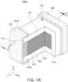
- a multilayer ceramic capacitor 100a may include a body 110, a first external electrode 131, and a second external electrode 132.
- the body 110 may include a capacitance region 115 in which a first internal electrode 121 and a second internal electrode 122 are alternately stacked in the first direction (e.g., the T direction) with a dielectric layer 111 interposed therebetween.
- the body 110 may be formed of a ceramic body by firing the capacitance region 115.
- the dielectric layer 111 is in a sintered state, and adjacent dielectric layers 111 may be integrated such that boundaries therebetween may not be readily apparent without using a scanning electron microscope (SEM).
- the body 110 may be formed of a hexahedron having both side surfaces in a length direction (L), both side surfaces in a width direction (W), and both side surfaces in a thickness direction (T), and the edges and/or corners of the hexahedron may be polished to be rounded.
- a shape and dimensions of the body 110 and the number of stacked dielectric layers 111 are not limited to those shown in the present exemplary embodiment.
- the thickness of the dielectric layer 111 may be changed according to a capacitance design of the multilayer ceramic capacitor 100a, and may include ceramic powder having a high permittivity, for example, barium titanate (BaTiO 3 )-based powder but is not limited thereto.
- various ceramic additives e.g., MgO, Al 2 O 3 , SiO 2 , and ZnO
- organic solvents e.g., organic solvents, plasticizers, binders, dispersants, etc.
- An average particle diameter of the ceramic powder used to form the dielectric layer 111 is not particularly limited and may be adjusted according to the required specifications of the multilayer ceramic capacitor 100a (e.g., miniaturization and/or high capacitance are required for capacitors for electronic devices, and high withstand voltage characteristics and/or high strength are required for capacitors for electric devices).
- the average particle diameter of the ceramic powder may be adjusted to 400 nm or less.
- the dielectric layer 111 may be formed by applying a slurry including powder, such as barium titanate (BaTiO 3 ), on a carrier film and drying the slurry to form a plurality of ceramic sheets.
- the ceramic sheet may be formed by preparing a slurry by mixing ceramic powder, a binder, and a solvent and forming the slurry as a sheet having a thickness of several um by a doctor blade method, but is not limited thereto.
- the first internal electrode 121 and the second internal electrode 122 may be formed by printing a conductive paste including a conductive metal such that the first internal electrode 121 and the second internal electrode 122 are alternately exposed to one side surface and the other side surface of the body 110 in the length direction L in the stack direction (e.g., T direction), and the first internal electrode 121 and the second internal electrode 122 may be electrically insulated from each other by the dielectric layer interposed therebetween.
- each of the first internal electrode 121 and the second internal electrode 122 may be formed of a conductive paste for internal electrodes including 40 wt% to 50 wt% of conductive metal powder having an average particle size of 0.1 um to 0.2 um, but is not limited thereto.
- the conductive paste may be nickel (Ni), copper (Cu), palladium (Pd), silver (Ag), lead (Pb) or platinum (Pt) alone or alloys thereof, and the present disclosure is not limited thereto.
- internal electrode patterns may be formed by applying the conductive paste for internal electrodes on the ceramic sheet by a printing method or the like.
- a screen-printing method, a gravure printing method, an inkjet printing method, and the like may be used as a printing method of the conductive paste, but the present disclosure is not limited thereto.
- 200 to 300 ceramic sheets on which the internal electrode patterns are printed may be stacked, pressed, and fired to form the body 110.
- Capacitance of the multilayer ceramic capacitor 100a may be proportional to an overlapping area of the first internal electrode 121 and the second internal electrode 122 in the stacking direction (e.g., T direction), may be proportional to a total stack number of the first internal electrode 121 and the second internal electrode 122, and may be inversely proportional to an interval between the first internal electrode 121 and the second internal electrode 122.
- the interval between the internal electrodes may be substantially equal to a thickness of one dielectric layer 111.
- the multilayer ceramic capacitor 100a may have a larger capacitance compared to a thickness thereof as the interval between the first internal electrode 121 and the second internal electrode 122 is reduced. Meanwhile, a withstand voltage of the multilayer ceramic capacitor 100a may be higher as the interval between the internal electrodes is longer. Therefore, the interval between the internal electrodes may be adjusted according to required standards of the multilayer ceramic capacitor 100a (e.g., miniaturization and/or high capacitance are required for capacitors for electronic devices, and high withstand voltage characteristics and/or high strength are required for capacitors for electric devices). The thickness of each of the first internal electrode 121 and the second internal electrode 122 may also be affected by the interval between the internal electrodes.
- the multilayer ceramic capacitor 100a may be designed so that the interval between the first internal electrode 121 and the second internal electrode 122 exceeds twice a thickness of each of the first internal electrode 121 and the second internal electrode 122.
- the multilayer ceramic capacitor 100a may be designed so that the thickness of each of the first internal electrode 121 and the second internal electrode 122 is 0.4 um or less and the total number of layers is 400 or more.
- the first and second external electrodes 131 and 132 may be spaced apart from each other with the capacitance region 115 therebetween in a second direction (e.g., the L direction) different from the first direction (e.g., the T direction) on the body, and may be connected to each of the first internal electrode 121 and the second internal electrode 122.
- a second direction e.g., the L direction
- first direction e.g., the T direction
- each of the first and second external electrodes 131 and 132 may be formed by dipping into a paste including a metal component, a method of printing a conductive paste, a sheet transfer, or a pad transfer method, sputter plating, or electrolytic plating.
- the first and second external electrodes 131 and 132 may include a fired layer formed by firing the paste and a plating layer formed on an outer surface of the fired layer, and may further include a conductive resin layer between the fired layer and the plating layer.
- the conductive resin layer may be formed by including conductive particles in a thermosetting resin, such as epoxy.
- the metal component may be copper (Cu), nickel (Ni), palladium (Pd), platinum (Pt), gold (Au), silver (Ag), lead (Pb), tin (Sn) alone or alloys thereof, but is not limited thereto.
- the multilayer ceramic capacitor 100a may be mounted or embedded in an external substrate (e.g., a printed circuit board), and may be connected to at least one of wiring, land, solder, and bumps of the external substrate through the first and second external electrodes 131 and 132 to be electrically connected to a circuit (e.g., an integrated circuit or a processor) electrically connected to the external substrate.
- an external substrate e.g., a printed circuit board
- a circuit e.g., an integrated circuit or a processor
- the body 110 may include at least one of a plurality of cover layers 112 and 113 and a plurality of margin regions 114.
- the plurality of cover layers 112 and 113 may be disposed to sandwich the capacitance region 115 therebetween in the first direction (e.g., T direction) .
- Each of the plurality of cover layers 112 and 113 may be thicker than one dielectric layer 111 and may provide upper and lower surfaces of the body 110.
- a portion of each of the first and second external electrodes 131 and 132 may be disposed on a lower and/or upper surface of the body 110.
- the plurality of cover layers 112 and 113 may prevent external environmental factors (e.g., moisture, plating solution, and foreign matter) from penetrating into the capacitance region 115, protect the body 110 from external impact, and improve bending strength of the body 110.
- the plurality of cover layers 112 and 113 may include the same material as that of the dielectric layer 111 (e.g., a ferroelectric material, such as barium titanate).
- the plurality of margin regions 114 may be arranged to sandwich the capacitance region 115 therebetween in a third direction (e.g., the W direction), different from the first and second directions (e.g., the T and L directions). Since the plurality of margin regions 114 may prevent the first internal electrode 121 and the second internal electrode 122 from being exposed to the surface of the body 110 in the third direction (e.g., the W direction), external environmental factors (e.g., moisture, a plating solution, foreign matter) may be prevented from penetrating into the first internal electrode 121 and the second internal electrode 122 through the surface in the third direction, and the reliability and lifespan of the multilayer ceramic capacitor 100a may be improved.
- a third direction e.g., the W direction
- external environmental factors e.g., moisture, a plating solution, foreign matter
- the plurality of margin regions 114 may contribute to improving capacitance of the multilayer ceramic capacitor 100a by increasing an overlapping area of the internal electrode 121 and the second internal electrode 122.
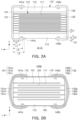
- one of the plurality of cover layers 112 and 113 may have a plurality of depressions 141a, 141b, 142a, and 142b in positions spaced apart from second outer surfaces of one of the plurality of cover layers 112 and 113 in the second direction (e.g., the L direction).
- the plurality of depressions 141a, 141b, 142a, and 142b may be formed on first outer surfaces of the plurality of cover layers 112 and 113 in the first direction (e.g., the T direction) .
- one of the plurality of cover layers 112 and 113 may have a plurality of depressions 141a and 142a, and the other of the plurality of cover layers 112 and 113 may have a plurality of depressions 141b and 142b.
- a body 110p before firing may be deformed to a body 110c in a first state by firing (heat treatment).
- the capacitance region 115 of the body 110c may be contracted more than the plurality of cover layers 112 and 113, and the plurality of cover layers 112 and 113 may be subjected to shear stress due to relative contraction of the capacitance region 115.
- the plurality of depressions 141a, 141b, 142a, and 142b may disperse the shear stress, concentration of the shear stress at a specific point (e.g., the second outer surfaces in the second direction) of the plurality of cover layers 112 and 113 may be prevented. Concentration of the shear stress may cause cracks or delamination. According to the shear stress dispersing action of the plurality of depressions 141a, 141b, 142a, and 142b, a shape of the plurality of depressions 141a, 141b, 142a, and 142b may also be deformed (for example, deformation of a difference between an upper width and a lower width).
- the body 110p before firing may be deformed to a body 110d in a second state.
- the plurality of cover layers 112 and 113 of the body 110d may contract more than the capacitance region 115 and may be subjected to shear stress due to the relative contraction. Since the plurality of depressions 141a, 141b, 142a, and 142b may disperse the shear stress, concentration of the shear stress at a specific point of the plurality of cover layers 112 and 113 may be prevented. Concentration of the shear stress may cause cracks or delamination.
- a shape of the plurality of depressions 141a, 141b, 142a, and 142b may also be deformed (for example, deformation of a difference between an upper width and a lower width).
- the multilayer ceramic capacitor 100a may have a structure that reduces a possibility of occurrence of defects (e.g., cracks, delamination) and may be stably manufactured.
- a thickness T1 of one dielectric layer 111 may vary according to an overall size of the multilayer ceramic capacitor 100a, and the thickness T1 of one dielectric layer 111 and/or the overall size of the multilayer ceramic capacitor 100a may affect the shrinkage relationship between the capacitance region 115 and the plurality of cover layers 112 and 113. Accordingly, it may be difficult to accurately predict the shrinkage relationship between the capacitance region 115 and the plurality of cover layers 112 and 113.
- the multilayer ceramic capacitor 100a may have a structure that may be stably manufactured even in a state in which the shrinkage relationship between the capacitance region 115 and the plurality of cover layers 112 and 113 is not accurately known, and may provide a higher degree of design freedom.
- each of the plurality of depressions 141a, 141b, 142a, and 142b may extend in the third direction (e.g., the W direction) (which may be expressed as a ditch shape) different from the first and second directions.
- a difference in shrinkage rate between the plurality of cover layers 112 and 113 and the capacitance region 115 may be due to a difference between stack structures therein in the first direction, and a difference (corresponding to isotropy) between a shrinkage length of the capacitance region 115 and a shrinkage length of the capacitance region 115 in the second and third directions may be different from that of the plurality of cover layers 112 and 113.
- a shrinkage behavior of the plurality of cover layers 112 and 113 may be close to an isotropic shrinkage behavior, and a shrinkage behavior of the capacitance region 115 may be close to an anisotropic shrinkage behavior.
- each of the plurality of depressions 141a, 141b, 142a, and 142b may be different from the first direction
- the plurality of depressions 141a, 141b, 142a, and 142b may cancel out the difference between the shrinkage length in the first direction and the shrinkage length in the second and third directions. Accordingly, the shear stress dispersion efficiency of the plurality of depressions 141a, 141b, 142a, and 142b may be further improved.
- the plurality of depressions 141a, 141b, 142a, and 142b may not extend to be formed in outer surfaces of the plurality of margin regions 114 in the third direction (e.g., the W direction) .
- the effect of depressions on the outer surfaces of the plurality of margin regions 114 in the third direction on dispersing the shear stress of the body 110 may be smaller than that of the plurality of depressions 141a, 141b, 142a, and 142b.
- the plurality of margin regions 114 may not have depressions and may be designed to focus more on increasing reliability improvement efficiency compared to an overall thickness of the plurality of margin regions 114.
- the bending length L3 of each of the first and second external electrodes 131 and 132 in the second direction may be a length from second outer surfaces of the plurality of cover layers 112 and 113 in the second direction (e.g., the L direction) to the edge of each of the first and second external electrodes 131 and 132 in the second direction (e.g., the L direction).
- a difference between the bending length L3 and the longest distance L4 in the second direction may be appropriately determined in consideration of a difference (process distribution) between the design and actual formation of the first and second external electrodes 131 and 132.
- the plurality of depressions 141a, 141b, 142a, and 142b may be stably covered by the first and second external electrodes 131 and 132, the plurality of depressions 141a, 141b, 142a, and 142b may be stably protected from external physical collision by the first and second external electrodes 131 and 132. Accordingly, external shock protection performance or overall strength of the plurality of cover layers 112 and 113 may be further improved.
- each of the plurality of depressions 141a, 141b, 142a, and 142b may overlap the first internal electrode 121 and the second internal electrode 122 in the first direction (e.g., the T direction).
- the shortest distance L1 from the second outer surfaces of the plurality of cover layers 112 and 113 in the second direction (e.g., the L direction) to a closer one of the plurality of depressions 141a, 141b, 142a, and 142b may be longer than a distance L2 between the second internal electrode 122 and the first external electrode 131 in the second direction (e.g., the L direction) and may be longer than a distance between the first internal electrode 121 and the second external electrode 132 in the second direction.
- a difference between the shortest distance L1 and the distance L2 may be appropriately determined in consideration of the total stack number of the first internal electrode 121 and the second internal electrode 122 or a size of the body 110.
- a portion between the second internal electrode 122 and the first external electrode 131 and a portion between the first internal electrode 121 and the second external electrode 132 may be expressed as an L-margin, and may be a potion in which the total stack number of the internal electrodes is half, compared to a central portion of the capacitance region 115.
- the body 110 may be compressed in the first direction (e.g., the T direction) during a manufacturing process, and a difference of the total stack number of the internal electrodes between the L-margin and the central portion may cause a step difference between the L-margin and the central portion during the compressing process.
- a portion of the plurality of cover layers 112 and 113 overlapping the L-margin in the first direction may absorb a step difference between the L-margin and the central portion during the compression process. Accordingly, since the body 110 may have a more stable structure, overall reliability or strength of the body 110 may be further improved.
- each of the plurality of depressions 141a, 141b, 142a, and 142b is greater than the thickness T1 of one dielectric layer 111 and may be smaller than the thickness of one of the plurality of cover layers 112 and 113.
- the overall size (corresponding to T2) of each of the plurality of depressions 141a, 141b, 142a, and 142b may be a size of the degree due to the addition of a separate process for forming the plurality of depressions 141a, 141b, 142a, and 142b but is not limited thereto.
- a relationship between a depth T2 of each of the plurality of depressions 141a, 141b, 142a, and 142b and a thickness T3 of each of the first and second external electrodes 131 and 132 may vary depending on the overall size of the multilayer ceramic capacitor 100a or a specific shape of the first and second external electrodes 131 and 132.
- a plurality of compression plates 40a and 40b each including a plurality of protrusions 41a, 41b, 42a, and 42b may compress first outer surfaces of cover layers 112p and 113p in which a plurality of depressions are not formed. Accordingly, the first outer surfaces of the cover layers 112p and 113p may be deformed, and a plurality of depressions may be formed.
- the compression may be performed before firing (heat treatment).
- lasers may be irradiated to the first outer surfaces of the cover layers 112p and 113p on which the plurality of depressions are not formed. Accordingly, portions of the cover layers 112p and 113p may be removed, and a plurality of depressions may be formed.
- the irradiation may be performed before firing (heat treatment).
- a portion of the first external electrode 131 may be disposed inside of one of the plurality of depressions 141a, 141b, 142a, and 142b, and a portion of the second external electrode 132 may be disposed inside of the other one of the plurality of depressions 141a, 141b, 142a, and 142b.
- a gap between the body 110 and the first and second external electrodes 131 and 132 may be a path through which external moisture or foreign matter penetrate. Since the plurality of depressions 141a, 141b, 142a, and 142b may bend the path at least four times, moisture penetrating into the gap between the body 110 and the first and second external electrodes 131 and 132 is stably prevented. Therefore, the multilayer ceramic capacitor 100a according to an exemplary embodiment in the present disclosure may have improved reliability by stably blocking the penetration of external moisture or foreign matter.
- the base electrode layers 131a and 132a may be formed by dipping a portion of the body 110 in a paste including a metal material and/or glass frit or firing in a state in which the paste is printed on a portion of the body 110, or may be formed by a sheet transfer or a pad transfer method.
- the metal material may be copper (Cu) to improve electrical connectivity with respect to the body 110 but is not limited thereto.
- the metal material may include at least one of copper (Cu), nickel (Ni), palladium (Pd), platinum (Pt), gold (Au), silver (Ag), and lead (Pb), may vary depending on a metal material of the internal electrodes in the body 110.
- the plating layers 131c and 132c may be formed by sputtering or electroplating but are not limited thereto.
- the plating layers 131c and 132c may include an inner plating layer including nickel (Ni) and an outer plating layer including tin (Sn).
- the conductive resin layers 131b and 132b may include a thermosetting resin, such as epoxy, and a plurality of conductive particles (e.g., the same metal material as the base electrode layer).
- a thermosetting resin such as epoxy
- a plurality of conductive particles e.g., the same metal material as the base electrode layer.
- the thermosetting resin it is not limited to the thermosetting resin, and the conductive resin layers 131b and 132b may include a bisphenol A resin, a glycol epoxy resin, a novolak epoxy resin, or a resin that is liquid at room temperature due to a low molecular weight thereof.
- the conductive resin layers 131b and 132b may improve durability of the first and second external electrodes 131 and 132 against external impact or prevent penetration of external moisture or a plating solution into the body 110. Therefore, the conductive resin layers 131b and 132b may reduce a rate at which the reliability of the first and second external electrodes 131 and 132 deteriorates even when the first and second external electrodes 131 and 132 are exposed to harsh environments.
- the coating layer 150 may cover the first and second outer surfaces of the plurality of cover layers 112 and 113, and may further cover portions of the first and second external electrodes 131 and 132 and/or outer surfaces of the plurality of margin regions according to design.
- the coating layer 150 may be formed of organic/inorganic compounds including Si to improve moisture resistance reliability of the body 110, and may be formed of organic/inorganic substances including fluorine (F) and polymer components.
- the coating layer 150 may be implemented as a silane coupling agent or silicone-resin to have water repellency.
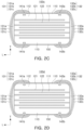
- each of the plurality of depressions 141a, 141b, 142a, and 142b may have a constant width.
- a shape of the plurality of depressions 141a, 141b, 142a, and 142b before firing (heat treatment) may be close to the shape of the plurality of depressions 141a, 141b, 142a, and 142b of FIG. 2D .
- the shape of the plurality of depressions 141a, 141b, 142a, and 142b before firing (heat treatment) may be close to the shape of the plurality of depressions 141a, 141b, 142a, and 142b of FIG. 2C .
- the width of each of the plurality of depressions 141a, 141b, 142a, and 142b may increase inwardly of each of the plurality of depressions 1411a, 141b, 142a, and 142b from the first outer surface of one of the plurality of cover layers 112 and 113 in the first direction (e.g., the T direction).
- the shape of the plurality of depressions 141a, 141b, 142a, and 142b before firing (heat treatment) may be close to the shape of the plurality of depressions 141a, 141b, 142a, and 142b of FIG. 2B .
- the width of each of the plurality of depressions 141a, 141b, 142a, and 142b may decrease inwardly of each of the plurality of depressions 141a, 141b, 142a, and 142b from the first outer surface of one of the plurality of cover layers 141a, 141b, 142a, and 142b in the first direction (e.g., the T direction) .
- the shape of the plurality of depressions 141a, 141b, 142a, and 142b before firing (heat treatment) may be close to the shape of the plurality of depressions 141a, 141b, 142a, and 142b of FIG. 2B .
- L1, L2, L3, L4, T1, T2, and T3 in the present specification may be measured as an average value of portions corresponding to L1, L2, L3, L4, T1, T2, and T3 in an L-T cross-section of the multilayer ceramic capacitor (including the center of the multilayer ceramic capacitor) formed by polishing the multilayer ceramic capacitor in the W direction.
- the L-T section may be applied to analysis using at least one of transmission electron microscopy (TEM), atomic force microscope (AFM), scanning electron microscope (SEM), an optical microscope, and a surface profiler, and L1, L2, L3, L4, T1, T2, and T3 may be measured by visual confirmation or image processing of an image obtained according to the above analysis (e.g., identifying pixels based on color or brightness of the pixels, filtering pixel values for pixel identification efficiency, integration of distances between identified pixels, etc.).
- TEM transmission electron microscopy
- AFM atomic force microscope
- SEM scanning electron microscope
- an optical microscope e.g., a surface profiler
- L1, L2, L3, L4, T1, T2, and T3 may be measured by visual confirmation or image processing of an image obtained according to the above analysis (e.g., identifying pixels based on color or brightness of the pixels, filtering pixel values for pixel identification efficiency, integration of distances between identified pixels, etc.).
- the multilayer ceramic capacitor according to an exemplary embodiment in the present disclosure may have a structure that reduces a possibility of the occurrence of defects (e.g., cracks, delamination) and may be stably manufactured.
- defects e.g., cracks, delamination
- the multilayer ceramic capacitor may have a structure that may be stably manufactured even in a state in which it is difficult to accurately know internal shrinkage characteristics and provide a higher degree of freedom in design.
- the multilayer ceramic capacitor may have improved reliability by stably blocking penetration of external moisture or foreign matter.
- the multilayer ceramic capacitor may have a stable structure by absorbing an internal step difference.
Landscapes
- Engineering & Computer Science (AREA)
- Power Engineering (AREA)
- Microelectronics & Electronic Packaging (AREA)
- Manufacturing & Machinery (AREA)
- Chemical & Material Sciences (AREA)
- Ceramic Engineering (AREA)
- Inorganic Chemistry (AREA)
- Fixed Capacitors And Capacitor Manufacturing Machines (AREA)
- Ceramic Capacitors (AREA)
Applications Claiming Priority (1)
| Application Number | Priority Date | Filing Date | Title |
|---|---|---|---|
| KR1020220173424A KR20240088063A (ko) | 2022-12-13 | 2022-12-13 | 적층 세라믹 커패시터 |
Publications (2)
| Publication Number | Publication Date |
|---|---|
| EP4386789A2 true EP4386789A2 (de) | 2024-06-19 |
| EP4386789A3 EP4386789A3 (de) | 2024-08-07 |
Family
ID=89029695
Family Applications (1)
| Application Number | Title | Priority Date | Filing Date |
|---|---|---|---|
| EP23213312.4A Pending EP4386789A3 (de) | 2022-12-13 | 2023-11-30 | Keramischer mehrschichtkondensator mit einer vertiefung der äusseren elektroden, die das eindringen von äusserer feuchtigkeit oder fremdstoffen blockiert |
Country Status (5)
| Country | Link |
|---|---|
| US (1) | US12580129B2 (de) |
| EP (1) | EP4386789A3 (de) |
| JP (1) | JP2024084723A (de) |
| KR (1) | KR20240088063A (de) |
| CN (1) | CN118197803A (de) |
Family Cites Families (13)
| Publication number | Priority date | Publication date | Assignee | Title |
|---|---|---|---|---|
| JPS6096813U (ja) * | 1983-12-09 | 1985-07-02 | 関西日本電気株式会社 | 積層セラミツクコンデンサ |
| JPH0238722U (de) * | 1988-09-06 | 1990-03-15 | ||
| JPH0845777A (ja) * | 1994-08-04 | 1996-02-16 | Matsushita Electric Ind Co Ltd | チップ形積層セラミックコンデンサ |
| JP2007067026A (ja) * | 2005-08-30 | 2007-03-15 | Taiyo Yuden Co Ltd | 電子部品及び電子部品の製造方法 |
| JP5228890B2 (ja) | 2008-12-24 | 2013-07-03 | 株式会社村田製作所 | 電子部品およびその製造方法 |
| JP4511625B1 (ja) | 2009-10-16 | 2010-07-28 | ルビコン株式会社 | 積層コンデンサ、その製造方法、回路基板および電子機器 |
| KR101141402B1 (ko) * | 2011-03-09 | 2012-05-03 | 삼성전기주식회사 | 적층 세라믹 커패시터 및 그 제조방법 |
| KR20130123661A (ko) * | 2012-05-03 | 2013-11-13 | 삼성전기주식회사 | 적층 세라믹 전자부품 및 그 제조 방법 |
| KR101525666B1 (ko) | 2013-07-11 | 2015-06-03 | 삼성전기주식회사 | 적층 세라믹 커패시터 및 그 제조 방법 |
| JP6378122B2 (ja) | 2014-12-05 | 2018-08-22 | 太陽誘電株式会社 | 積層セラミック電子部品 |
| JP2017037930A (ja) * | 2015-08-07 | 2017-02-16 | 株式会社村田製作所 | セラミック電子部品の製造方法及びセラミック電子部品 |
| JP6793027B2 (ja) * | 2016-12-16 | 2020-12-02 | 太陽誘電株式会社 | 積層セラミック電子部品 |
| KR102620541B1 (ko) * | 2018-08-22 | 2024-01-03 | 삼성전기주식회사 | 커패시터 부품 |
-
2022
- 2022-12-13 KR KR1020220173424A patent/KR20240088063A/ko active Pending
-
2023
- 2023-11-30 EP EP23213312.4A patent/EP4386789A3/de active Pending
- 2023-12-11 JP JP2023208561A patent/JP2024084723A/ja active Pending
- 2023-12-12 CN CN202311695953.XA patent/CN118197803A/zh active Pending
- 2023-12-12 US US18/537,482 patent/US12580129B2/en active Active
Also Published As
| Publication number | Publication date |
|---|---|
| KR20240088063A (ko) | 2024-06-20 |
| CN118197803A (zh) | 2024-06-14 |
| JP2024084723A (ja) | 2024-06-25 |
| US12580129B2 (en) | 2026-03-17 |
| US20240194409A1 (en) | 2024-06-13 |
| EP4386789A3 (de) | 2024-08-07 |
Similar Documents
| Publication | Publication Date | Title |
|---|---|---|
| CN110289166B (zh) | 多层陶瓷电子组件和多层陶瓷电子组件封装件 | |
| CN112542318B (zh) | 多层陶瓷电子组件 | |
| KR20260020160A (ko) | 유전체 조성물 및 이를 포함하는 적층형 커패시터 | |
| CN111199831B (zh) | 多层陶瓷电子组件 | |
| EP4390991A2 (de) | Mehrschichtiger keramischer kondensator (mlcc) mit seitlichen dielektrischen schichten, die kristalle unterschiedlicher grösse enthalten | |
| EP4386789A2 (de) | Keramischer mehrschichtkondensator mit einer vertiefung der äusseren elektroden, die das eindringen von äusserer feuchtigkeit oder fremdstoffen blockiert | |
| CN111180207B (zh) | 多层陶瓷电子组件和多层陶瓷电子组件封装件 | |
| US11948745B2 (en) | Multilayer capacitor | |
| US12444535B2 (en) | Multilayer ceramic capacitor | |
| US20240274365A1 (en) | Multilayer ceramic capacitor | |
| KR102950443B1 (ko) | 적층형 커패시터 | |
| US12394569B2 (en) | Multilayer capacitor | |
| US12142435B2 (en) | Multilayer capacitor | |
| KR102449363B1 (ko) | 적층 세라믹 전자부품 | |
| CN116246886A (zh) | 多层电容器和制造多层电容器的方法 |
Legal Events
| Date | Code | Title | Description |
|---|---|---|---|
| PUAI | Public reference made under article 153(3) epc to a published international application that has entered the european phase |
Free format text: ORIGINAL CODE: 0009012 |
|
| STAA | Information on the status of an ep patent application or granted ep patent |
Free format text: STATUS: THE APPLICATION HAS BEEN PUBLISHED |
|
| AK | Designated contracting states |
Kind code of ref document: A2 Designated state(s): AL AT BE BG CH CY CZ DE DK EE ES FI FR GB GR HR HU IE IS IT LI LT LU LV MC ME MK MT NL NO PL PT RO RS SE SI SK SM TR |
|
| PUAL | Search report despatched |
Free format text: ORIGINAL CODE: 0009013 |
|
| AK | Designated contracting states |
Kind code of ref document: A3 Designated state(s): AL AT BE BG CH CY CZ DE DK EE ES FI FR GB GR HR HU IE IS IT LI LT LU LV MC ME MK MT NL NO PL PT RO RS SE SI SK SM TR |
|
| RIC1 | Information provided on ipc code assigned before grant |
Ipc: H01G 4/248 20060101ALI20240702BHEP Ipc: H01G 4/224 20060101ALI20240702BHEP Ipc: H01G 4/012 20060101ALI20240702BHEP Ipc: H01G 4/40 20060101ALI20240702BHEP Ipc: H01G 4/38 20060101ALI20240702BHEP Ipc: H01G 4/32 20060101ALI20240702BHEP Ipc: H01G 4/30 20060101ALI20240702BHEP Ipc: H01G 4/232 20060101ALI20240702BHEP Ipc: H01G 4/228 20060101ALI20240702BHEP Ipc: H01G 4/18 20060101ALI20240702BHEP Ipc: H01G 4/12 20060101ALI20240702BHEP Ipc: H01G 2/10 20060101ALI20240702BHEP Ipc: H01G 2/02 20060101AFI20240702BHEP |
|
| STAA | Information on the status of an ep patent application or granted ep patent |
Free format text: STATUS: REQUEST FOR EXAMINATION WAS MADE |
|
| 17P | Request for examination filed |
Effective date: 20250107 |