EP4386484A1 - Verfahren zur strukturierung eines substrats, verfahren zur herstellung einer mikrostruktur auf einem substrat und verfahren zur herstellung einer fluidischen vorrichtung - Google Patents
Verfahren zur strukturierung eines substrats, verfahren zur herstellung einer mikrostruktur auf einem substrat und verfahren zur herstellung einer fluidischen vorrichtung Download PDFInfo
- Publication number
- EP4386484A1 EP4386484A1 EP22855863.1A EP22855863A EP4386484A1 EP 4386484 A1 EP4386484 A1 EP 4386484A1 EP 22855863 A EP22855863 A EP 22855863A EP 4386484 A1 EP4386484 A1 EP 4386484A1
- Authority
- EP
- European Patent Office
- Prior art keywords
- substrate
- target material
- hydrophobic film
- patterning
- microstructure
- Prior art date
- Legal status (The legal status is an assumption and is not a legal conclusion. Google has not performed a legal analysis and makes no representation as to the accuracy of the status listed.)
- Pending
Links
Images

Classifications
-
- B—PERFORMING OPERATIONS; TRANSPORTING
- B01—PHYSICAL OR CHEMICAL PROCESSES OR APPARATUS IN GENERAL
- B01L—CHEMICAL OR PHYSICAL LABORATORY APPARATUS FOR GENERAL USE
- B01L3/00—Containers or dishes for laboratory use, e.g. laboratory glassware; Droppers
- B01L3/50—Containers for the purpose of retaining a material to be analysed, e.g. test tubes
- B01L3/502—Containers for the purpose of retaining a material to be analysed, e.g. test tubes with fluid transport, e.g. in multi-compartment structures
- B01L3/5027—Containers for the purpose of retaining a material to be analysed, e.g. test tubes with fluid transport, e.g. in multi-compartment structures by integrated microfluidic structures, i.e. dimensions of channels and chambers are such that surface tension forces are important, e.g. lab-on-a-chip
- B01L3/502707—Containers for the purpose of retaining a material to be analysed, e.g. test tubes with fluid transport, e.g. in multi-compartment structures by integrated microfluidic structures, i.e. dimensions of channels and chambers are such that surface tension forces are important, e.g. lab-on-a-chip characterised by the manufacture of the container or its components
-
- C—CHEMISTRY; METALLURGY
- C23—COATING METALLIC MATERIAL; COATING MATERIAL WITH METALLIC MATERIAL; CHEMICAL SURFACE TREATMENT; DIFFUSION TREATMENT OF METALLIC MATERIAL; COATING BY VACUUM EVAPORATION, BY SPUTTERING, BY ION IMPLANTATION OR BY CHEMICAL VAPOUR DEPOSITION, IN GENERAL; INHIBITING CORROSION OF METALLIC MATERIAL OR INCRUSTATION IN GENERAL
- C23C—COATING METALLIC MATERIAL; COATING MATERIAL WITH METALLIC MATERIAL; SURFACE TREATMENT OF METALLIC MATERIAL BY DIFFUSION INTO THE SURFACE, BY CHEMICAL CONVERSION OR SUBSTITUTION; COATING BY VACUUM EVAPORATION, BY SPUTTERING, BY ION IMPLANTATION OR BY CHEMICAL VAPOUR DEPOSITION, IN GENERAL
- C23C14/00—Coating by vacuum evaporation, by sputtering or by ion implantation of the coating forming material
- C23C14/04—Coating on selected surface areas, e.g. using masks
- C23C14/042—Coating on selected surface areas, e.g. using masks using masks
-
- B—PERFORMING OPERATIONS; TRANSPORTING
- B81—MICROSTRUCTURAL TECHNOLOGY
- B81C—PROCESSES OR APPARATUS SPECIALLY ADAPTED FOR THE MANUFACTURE OR TREATMENT OF MICROSTRUCTURAL DEVICES OR SYSTEMS
- B81C1/00—Manufacture or treatment of devices or systems in or on a substrate
- B81C1/00015—Manufacture or treatment of devices or systems in or on a substrate for manufacturing microsystems
- B81C1/00206—Processes for functionalising a surface, e.g. provide the surface with specific mechanical, chemical or biological properties
-
- C—CHEMISTRY; METALLURGY
- C23—COATING METALLIC MATERIAL; COATING MATERIAL WITH METALLIC MATERIAL; CHEMICAL SURFACE TREATMENT; DIFFUSION TREATMENT OF METALLIC MATERIAL; COATING BY VACUUM EVAPORATION, BY SPUTTERING, BY ION IMPLANTATION OR BY CHEMICAL VAPOUR DEPOSITION, IN GENERAL; INHIBITING CORROSION OF METALLIC MATERIAL OR INCRUSTATION IN GENERAL
- C23C—COATING METALLIC MATERIAL; COATING MATERIAL WITH METALLIC MATERIAL; SURFACE TREATMENT OF METALLIC MATERIAL BY DIFFUSION INTO THE SURFACE, BY CHEMICAL CONVERSION OR SUBSTITUTION; COATING BY VACUUM EVAPORATION, BY SPUTTERING, BY ION IMPLANTATION OR BY CHEMICAL VAPOUR DEPOSITION, IN GENERAL
- C23C14/00—Coating by vacuum evaporation, by sputtering or by ion implantation of the coating forming material
- C23C14/02—Pretreatment of the material to be coated
- C23C14/024—Deposition of sublayers, e.g. to promote adhesion of the coating
-
- C—CHEMISTRY; METALLURGY
- C23—COATING METALLIC MATERIAL; COATING MATERIAL WITH METALLIC MATERIAL; CHEMICAL SURFACE TREATMENT; DIFFUSION TREATMENT OF METALLIC MATERIAL; COATING BY VACUUM EVAPORATION, BY SPUTTERING, BY ION IMPLANTATION OR BY CHEMICAL VAPOUR DEPOSITION, IN GENERAL; INHIBITING CORROSION OF METALLIC MATERIAL OR INCRUSTATION IN GENERAL
- C23C—COATING METALLIC MATERIAL; COATING MATERIAL WITH METALLIC MATERIAL; SURFACE TREATMENT OF METALLIC MATERIAL BY DIFFUSION INTO THE SURFACE, BY CHEMICAL CONVERSION OR SUBSTITUTION; COATING BY VACUUM EVAPORATION, BY SPUTTERING, BY ION IMPLANTATION OR BY CHEMICAL VAPOUR DEPOSITION, IN GENERAL
- C23C14/00—Coating by vacuum evaporation, by sputtering or by ion implantation of the coating forming material
- C23C14/04—Coating on selected surface areas, e.g. using masks
-
- C—CHEMISTRY; METALLURGY
- C23—COATING METALLIC MATERIAL; COATING MATERIAL WITH METALLIC MATERIAL; CHEMICAL SURFACE TREATMENT; DIFFUSION TREATMENT OF METALLIC MATERIAL; COATING BY VACUUM EVAPORATION, BY SPUTTERING, BY ION IMPLANTATION OR BY CHEMICAL VAPOUR DEPOSITION, IN GENERAL; INHIBITING CORROSION OF METALLIC MATERIAL OR INCRUSTATION IN GENERAL
- C23C—COATING METALLIC MATERIAL; COATING MATERIAL WITH METALLIC MATERIAL; SURFACE TREATMENT OF METALLIC MATERIAL BY DIFFUSION INTO THE SURFACE, BY CHEMICAL CONVERSION OR SUBSTITUTION; COATING BY VACUUM EVAPORATION, BY SPUTTERING, BY ION IMPLANTATION OR BY CHEMICAL VAPOUR DEPOSITION, IN GENERAL
- C23C14/00—Coating by vacuum evaporation, by sputtering or by ion implantation of the coating forming material
- C23C14/06—Coating by vacuum evaporation, by sputtering or by ion implantation of the coating forming material characterised by the coating material
- C23C14/14—Metallic material, boron or silicon
-
- C—CHEMISTRY; METALLURGY
- C23—COATING METALLIC MATERIAL; COATING MATERIAL WITH METALLIC MATERIAL; CHEMICAL SURFACE TREATMENT; DIFFUSION TREATMENT OF METALLIC MATERIAL; COATING BY VACUUM EVAPORATION, BY SPUTTERING, BY ION IMPLANTATION OR BY CHEMICAL VAPOUR DEPOSITION, IN GENERAL; INHIBITING CORROSION OF METALLIC MATERIAL OR INCRUSTATION IN GENERAL
- C23C—COATING METALLIC MATERIAL; COATING MATERIAL WITH METALLIC MATERIAL; SURFACE TREATMENT OF METALLIC MATERIAL BY DIFFUSION INTO THE SURFACE, BY CHEMICAL CONVERSION OR SUBSTITUTION; COATING BY VACUUM EVAPORATION, BY SPUTTERING, BY ION IMPLANTATION OR BY CHEMICAL VAPOUR DEPOSITION, IN GENERAL
- C23C14/00—Coating by vacuum evaporation, by sputtering or by ion implantation of the coating forming material
- C23C14/22—Coating by vacuum evaporation, by sputtering or by ion implantation of the coating forming material characterised by the process of coating
- C23C14/34—Sputtering
-
- C—CHEMISTRY; METALLURGY
- C23—COATING METALLIC MATERIAL; COATING MATERIAL WITH METALLIC MATERIAL; CHEMICAL SURFACE TREATMENT; DIFFUSION TREATMENT OF METALLIC MATERIAL; COATING BY VACUUM EVAPORATION, BY SPUTTERING, BY ION IMPLANTATION OR BY CHEMICAL VAPOUR DEPOSITION, IN GENERAL; INHIBITING CORROSION OF METALLIC MATERIAL OR INCRUSTATION IN GENERAL
- C23C—COATING METALLIC MATERIAL; COATING MATERIAL WITH METALLIC MATERIAL; SURFACE TREATMENT OF METALLIC MATERIAL BY DIFFUSION INTO THE SURFACE, BY CHEMICAL CONVERSION OR SUBSTITUTION; COATING BY VACUUM EVAPORATION, BY SPUTTERING, BY ION IMPLANTATION OR BY CHEMICAL VAPOUR DEPOSITION, IN GENERAL
- C23C14/00—Coating by vacuum evaporation, by sputtering or by ion implantation of the coating forming material
- C23C14/58—After-treatment
- C23C14/5846—Reactive treatment
- C23C14/5853—Oxidation
-
- B—PERFORMING OPERATIONS; TRANSPORTING
- B01—PHYSICAL OR CHEMICAL PROCESSES OR APPARATUS IN GENERAL
- B01L—CHEMICAL OR PHYSICAL LABORATORY APPARATUS FOR GENERAL USE
- B01L2200/00—Solutions for specific problems relating to chemical or physical laboratory apparatus
- B01L2200/06—Fluid handling related problems
- B01L2200/0647—Handling flowable solids, e.g. microscopic beads, cells, particles
-
- B—PERFORMING OPERATIONS; TRANSPORTING
- B01—PHYSICAL OR CHEMICAL PROCESSES OR APPARATUS IN GENERAL
- B01L—CHEMICAL OR PHYSICAL LABORATORY APPARATUS FOR GENERAL USE
- B01L2200/00—Solutions for specific problems relating to chemical or physical laboratory apparatus
- B01L2200/12—Specific details about manufacturing devices
-
- B—PERFORMING OPERATIONS; TRANSPORTING
- B01—PHYSICAL OR CHEMICAL PROCESSES OR APPARATUS IN GENERAL
- B01L—CHEMICAL OR PHYSICAL LABORATORY APPARATUS FOR GENERAL USE
- B01L2300/00—Additional constructional details
- B01L2300/08—Geometry, shape and general structure
- B01L2300/0896—Nanoscaled
-
- B—PERFORMING OPERATIONS; TRANSPORTING
- B01—PHYSICAL OR CHEMICAL PROCESSES OR APPARATUS IN GENERAL
- B01L—CHEMICAL OR PHYSICAL LABORATORY APPARATUS FOR GENERAL USE
- B01L2300/00—Additional constructional details
- B01L2300/12—Specific details about materials
-
- B—PERFORMING OPERATIONS; TRANSPORTING
- B01—PHYSICAL OR CHEMICAL PROCESSES OR APPARATUS IN GENERAL
- B01L—CHEMICAL OR PHYSICAL LABORATORY APPARATUS FOR GENERAL USE
- B01L2300/00—Additional constructional details
- B01L2300/16—Surface properties and coatings
- B01L2300/161—Control and use of surface tension forces, e.g. hydrophobic, hydrophilic
-
- B—PERFORMING OPERATIONS; TRANSPORTING
- B05—SPRAYING OR ATOMISING IN GENERAL; APPLYING FLUENT MATERIALS TO SURFACES, IN GENERAL
- B05D—PROCESSES FOR APPLYING FLUENT MATERIALS TO SURFACES, IN GENERAL
- B05D1/00—Processes for applying liquids or other fluent materials
- B05D1/32—Processes for applying liquids or other fluent materials using means for protecting parts of a surface not to be coated, e.g. using stencils, resists
- B05D1/322—Removable films used as masks
-
- B—PERFORMING OPERATIONS; TRANSPORTING
- B81—MICROSTRUCTURAL TECHNOLOGY
- B81B—MICROSTRUCTURAL DEVICES OR SYSTEMS, e.g. MICROMECHANICAL DEVICES
- B81B2201/00—Specific applications of microelectromechanical systems
- B81B2201/05—Microfluidics
- B81B2201/058—Microfluidics not provided for in B81B2201/051 - B81B2201/054
-
- B—PERFORMING OPERATIONS; TRANSPORTING
- B81—MICROSTRUCTURAL TECHNOLOGY
- B81B—MICROSTRUCTURAL DEVICES OR SYSTEMS, e.g. MICROMECHANICAL DEVICES
- B81B2207/00—Microstructural systems or auxiliary parts thereof
- B81B2207/05—Arrays
- B81B2207/056—Arrays of static structures
Definitions
- the present disclosure relates to a method for patterning a substrate, a method for forming a microstructure on a substrate, and a method for fabricating a fluidic device.
- microstructures or structures are formed on surfaces of substrates, such as wafers. Such a structure is formed partially or discretely on a surface of a substrate. On another portion of the surface of the substrate, no microstructure is formed, and the surface of the substrate is substantially exposed.
- structures or substances such as processing debris, particles or chemical contaminants, or growth or formation of non-specific substances, that are not necessarily desired are formed on or attached to the exposed substrate surface.
- the portion may be the surface of the original substrate or the surface of a film or layer disposed on the surface of the original substrate) be maintained or restored as clean as possible.
- a fluidic device including a microstructure in a flow channel.
- the microstructure is formed on the surface of the substrate, and a cover is brought into close contact with the surface of the substrate.
- a portion of the substrate surface with which the cover is brought into close contact must be free of a microstructure.
- the presence of an unwanted, accidentally formed microstructure, a contaminant such as particles, or the like can inhibit close contact between a portion of the surface of the substrate and the cover to deteriorate the sealing of the fluid contained therein.
- Desired is a method to avoid the formation or deposition of structures or materials that are not necessarily desired, such as processing debris, particles, or chemical contaminants, or the growth or formation of non-specific materials when a substrate is subjected to a process such as patterning or microstructure formation.
- a method for patterning a substrate includes patterning a hydrophobic film formed on a surface of a substrate, applying a target material, and oxidizing at least a surface of the applied target material.
- the method further includes removing the hydrophobic film from the substrate.
- substrate typically refers to a freely-selected substrate or a material surface formed on a substrate on which film processing is performed during a fabrication process.
- a surface of the substrate that can be subjected to processing contains a material, such as silicon (Si), silicon oxide (SiO 2 ), silicon-on-insulator (SOI), germanium (Ge), gallium arsenide (GaAs), glass, or sapphire.
- the surface of the substrate contains a semiconductor material or material commonly used in a semiconductor process.
- the surface of the substrate contains another material, such as a metal, a metal oxide, a metal alloy, or another conductive material, in accordance with the application.
- the surface of the substrate contains a polymer material.
- an oxide, a fat component, or the like may be present at an atomic level or a micro level.
- the substrate includes, but is not limited to, a semiconductor wafer, such as a silicon wafer, a glass wafer, or a polymer film.
- the substrate may be subjected to a pretreatment process to polish, etch, reduce, oxidize, hydroxylate, anneal, clean, and/or bake the substrate surface.
- the surface of the substrate contains such a material as a basic constituent material, and may contain impurities or include a surface layer when handled in the atmosphere or in a clean room environment, for example.
- the surface of the substrate may be partially or entirely hydrophobic. In some embodiments, the surface of the substrate may be partially or entirely hydrophilic.
- the surface of the substrate may be substantially planar.
- the surface of the substrate may include a flat surface. After at least the hydrophobic film is removed, the portion of the surface of the substrate may be flat.
- the portion of the surface of the substrate can be bonded to a member that defines a flow channel, thus creating a fluid-tight seal for the flow channel.
- the surface of the substrate may have a surface roughness of 5, 4, 3, 2, 0.5, 0.4, 0.3, 0.2, 0.1, 0.9, 0.8, 0.7, 0.6, 0.5, 0.4, 0.3, 0.2, or 0.1 nm Ra, or less than any of them.
- the surface of the substrate may have a surface roughness comparable to a commercially available or industrially usable substrate. For example, a commercially available silicon substrate, a glass substrate, or a polymer substrate, or a film may be used.
- hydrophobic film used in this specification refers to a film composed of a material having hydrophobicity (hydrophobic material, the same applies hereinafter) or containing a material having hydrophobicity on a surface thereof.
- the hydrophobic film may contain a fluorine compound or a resin.
- the hydrophobic film may be what is called a fluororesin film.
- the hydrophobic material may be selected from the group consisting of fluorinated polymers, fluorocarbon polymers, silicon polymers, and mixtures thereof.
- examples of the hydrophobic material include amorphous fluoropolymers (commercially available examples include the CYTOP (registered trademark) series, available from AGC Chemicals, having one of the following terminal functional groups.
- Examples thereof include those having one of the following terminal functional groups: A-type: -COON, M-type: -CONH-Si(OR), and S-type: -CF 3 ); polytetrafluoroethylene (commercially available examples include TEFLON (registered trademark) from Chemours); parylene; fluorinated hydrocarbons; fluoroacrylic copolymers (commercially available examples include FLUOROPEL (registered trademark) from Cytonix); fluorosilanes (such as trichloro(1H,1H,2H,2H-perfluorooctyl)silane (PFOTS) and perfluorodecyltrichlorosilane (FDTS); plasma-deposited fluorocarbons; polydimethylsiloxanes; other siloxanes; hydrophobic hydrocarbons such as 1-heptadecyne; and mixtures thereof.
- terminal functional groups such as TEFLON (registered trademark) from Chemour
- the hydrophobic material may be applied to at least part of the surface or the entire surface of the substrate.
- the hydrophobic material may be applied to the surface of the substrate by a dry or wet process.
- the hydrophobic material may be dropped and spin-coated on the surface of the substrate in a solution state. Then the hydrophobic material may be dried, heat treated, or baked.
- the hydrophobic film formed on the surface of the substrate is patterned.
- the hydrophobic film may be patterned using a photolithographic technique. A resist is applied to a surface of the plastic film with a spin coater or by spraying, prebaked, exposed to light, and developed. Thereby, the resist is patterned. The hydrophobic film is exposed at a location where the resist is removed. After the development, treatment such as rinsing and post-baking may be performed.
- patterning may include performing etching with a hard mask (e.g., a metal mask).
- a hard mask e.g., a metal mask
- the exposed surface of the hydrophobic film is subjected to an etching process.
- the hydrophobic film is patterned in correspondence with the pattern of the resist.
- An example of the etching of the hydrophobic film may be, but not particularly limited to, oxygen etching.
- the surface of the substrate is exposed.
- a target material is applied to the exposed surface of the substrate.
- the target material may be applied to the entire substrate, i.e., the surface of the resist.
- a film containing or consisting essentially of the target material may be formed.
- the target material examples include gold, platinum, aluminum, copper, iron, cobalt, silver, tin, indium, zinc, gallium, chromium, and oxides thereof.
- the target material may be an oxidizable material.
- the target material may be chromium (Cr).
- the target material may be zinc oxide (ZnO).
- the photoresist may be removed after the application of the target material. At this time, the target material applied to the surface of the photoresist may be removed together. This process may be referred to as a lift-off process. During the lift-off process, the hydrophobic film and the patterned target material may remain on the surface of the substrate.
- treatment may be performed on the applied target material.
- the treatment may be treatment for the surface of the target material.
- the treatment may be heating. Heating may include, for example, heating the substrate in a furnace or irradiating the target material or substrate with a laser.
- the treatment may be oxidation of at least the surface, or the whole or part of the volume of the target material. Examples of the oxidation include heating in an oxidizing atmosphere and plasma treatment.
- the target material may be processed or treated.
- a microstructure may be formed on the surface of the target material.
- the microstructure may be formed by etching the target material.
- the microstructure may be formed on the surface of the target material.
- a member for forming a microstructure may be grown on the surface of the target material.
- a nanowire may be formed on the surface of the target material.
- particles or a catalyst for growing the nanowire may be applied to a surface of a target material, and the nanowire may be grown from the surface as a starting point.
- the target material may be a material that can catalyze the growth of the nanowire or that can serve as a starting point for nanowire growth.
- Examples of the particles or a seed layer for forming the nanowire include ZnO and CrO.
- a nanowire using ZnO can be grown on the surface of any of these seed materials using a hydrothermal synthesis method.
- ZnO is first applied to a surface of the substrate (the surface of the target material).
- the substrate is immersed in a precursor solution in which zinc nitrate hexahydrate (Zn(NO 3 ) 2 ⁇ 6H 2 O) and hexamethylenetetramine (C 6 H 12 N 4 ) are dissolved in deionized water.
- ZnO nanowire can be grown on the surface of the target material.
- ZnO serves as particles for forming a nanowire. Therefore, it is not necessary to separately apply ZnO to the surface of the target material.
- Examples of the catalyst for producing a nanowire include gold, platinum, aluminum, copper, iron, cobalt, silver, tin, indium, zinc, gallium, chromium, and titanium.
- a nanowire using a catalyst can be produced by the following procedure.
- a covering layer may be formed on the surface of the nanowire.
- the covering layer can be formed by a vapor deposition method, such as sputtering, electron beam (EB) vapor deposition, physical vapor deposition (PVD), or an atomic layer deposition (ALD) apparatus.
- a vapor deposition method such as sputtering, electron beam (EB) vapor deposition, physical vapor deposition (PVD), or an atomic layer deposition (ALD) apparatus.
- the covering layer may be composed of a material having a high thermal conductivity.
- a device including a nanowire having such a covering layer can be used for heat-treating a sample.
- the covering layer may be composed of a material that can bind a peptide and/or nucleic acid and that has a high thermal conductivity.
- the surface of the nanowire can be modified with a peptide and/or a nucleic acid.
- the modified nanowire has the ability to efficiently capture or separate biomolecules from other substances.
- the hydrophobic film may be removed after processing of the target material, e.g., after processing, such as the heating or oxidation of the target material, or the formation of a microstructure.
- the hydrophobic film may be removed by the lift-off process.
- the hydrophobic film subjected to the heating or oxidation treatment is typically fragile.
- the hydrophobic film is peeled off from the substrate.
- removal of the hydrophobic film may be accelerated by, for example, ultrasonic cleaning.
- the hydrophobic film is then removed, thereby preparing the patterned target material (or a microstructure in addition thereto) on the surface of the substrate and a portion of the surface of the substrate free of the target material.
- the portion of the surface of the substrate thus exposed together with the patterning is substantially free of the target material or microstructure, etc.
- a clean substrate surface can be bonded to another substrate or member to create a fluid-tight bonding surface. It is thus possible to fabricate a highly sealed flow channel or fluidic device.
- a method for patterning a substrate, a method for forming a microstructure on a substrate, and a method for fabricating a fluidic device according to an embodiment of the present disclosure will be described.
- a nanowire of ZnO is grown in a patterned region, and a flow-channel device having the nanowire is fabricated. This is an example, and the present disclosure should not be construed as limited to this embodiment.
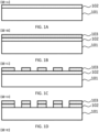
- a substrate 101 is provided, and a hydrophobic film 102 is formed on a surface thereof.
- the substrate 101 is typically a silicon substrate or a glass substrate used in a semiconductor process.
- the substrate 1101 may be cleaned in advance. Contaminants or particles can thereby be removed from the surface.
- the hydrophobic film 102 can be formed by spin coating.
- the hydrophobic film 102 formed by coating is baked.
- Cytop registered trademark, available from AGC Inc.
- a photoresist 103 is applied on the hydrophobic film 102.
- a material used in a semiconductor process can be used.
- AZ4903 available from Merck Performance Materials GmbH was used.
- the photoresist 103 is patterned.
- the photoresist 103 is prebaked. Exposure is performed so as to correspond to a pattern in which a target material will be formed later. Thereafter, development is performed.
- development for example, NMD-3 (available from Tokyo Ohka Kogyo Co., Ltd.) may be used.
- the substrate is rinsed with pure water and dried by nitrogen blowing.
- the photoresist 103 is post-baked. Thereby, the photoresist 103 has been patterned.
- portions of the hydrophobic film 102 that have been opened or exposed in Fig. 1C are etched.
- the hydrophobic film 102 may be subjected to oxygen etching.
- the etching apparatus may be an apparatus used in a typical semiconductor process.
- an RF plasma apparatus, TEP-01C2 ((available from Tateyama Machine Co., Ltd.) was used.
- TEP-01C2 (available from Tateyama Machine Co., Ltd.) was used.
- a target material 104 is applied or deposited to cover the entire substrate 101, i.e., the surfaces of the photoresist 103, including the portion of the surface of the substrate 101 exposed in Fig. 1D .
- chromium (Cr) was deposited as the target material 104 by sputter deposition to a thickness of more than 100 nm.
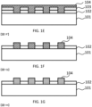
- the photoresist 103 and the target material 104 deposited on the photoresist 103 are removed by a lift-off process.
- the entire substrate 101 is immersed in heated 2-propanol for a predetermined time. Thereafter, ultrasonic cleaning was performed. Thereby, the target material 104 (chromium) was patterned on the substrate 101, and the other portion of the surface of the substrate 101 were covered with the hydrophobic film 102.
- the target material 104 is annealed.
- the target material 104 which was chromium, was maintained at 400°C in the air atmosphere and oxidized.
- the air atmosphere contains a sufficient amount of oxygen for the oxidation of chromium.
- the atmosphere during heating may be an oxidizing atmosphere.
- the surface of chromium may be oxidized by plasma treatment.
- ZnO nanowires 105 were grown as microstructures on the oxidized target material 104 (chromium).
- the ZnO nanowires 105 were formed by a hydrothermal synthesis method. If the hydrophobic film 102 does not cover the surface of the substrate 101, the nanowires 105 may also grow non-specifically on the surface of the substrate 101. As illustrated in Fig. 1H , since the hydrophobic film 102 covers the surface of the substrate 101, the nanowires 105 can grow only on the surfaces of the patterned target material 104.
- the substrate 101 includes the microstructures 105 (nanowires) formed at the positions of the target material 104 defined by the patterning.
- the microstructures 105 are not substantially present on the portion of the surface of the substrate 101 where the target material 104 is not present. In this way, the target material can be used as seed layers or starting points to form the microstructures only at the portions.
- a fluidic device 100 including the microstructures 105 formed as described above was fabricated.
- the fluidic device 100 mainly includes the substrate 101 and a cover (substrate) 111 bonded to the substrate 101.
- the substrate 101 is the substrate 101 illustrated in the Fig. 1I .
- the cover 111 includes a frame 112 and an internal space 120 surrounded by the frame 112 so as to cover the target material 104 and the microstructures 105 on the substrate 101.
- the frame 112 of the cover 111 is in close contact with the exposed the portion of the surface of the substrate 101 where the microstructures 105 are not present, forming a bonding interface 130.
- the bonding interface 130 is highly fluid-tight. This is because the portion of surface of the substrate 101 forming the bonding interface 130 has no non-specific growth of the microstructure 105 or the like, and has a flat surface substantially similar to the initial surface.
- the fluidic device 100 illustrated in Fig. 1J includes the substrate 101 having the target material 104 and the microstructures 105 thereon, and the cover 111 in close contact with the substrate 101 so as to enclose the microstructures 105.
- the substrate 101 and the cover 111 are in close contact with each other at the bonding interface 130 to form the internal space or a flow channel 120 containing the microstructures 105 therein.
- the flow channel 120 may have a plurality of target material pattern portions 104 and/or the microstructures 105.
- each flow channel may have a single target material pattern portion and/or a single microstructure.
- a single target material pattern portion 104 and/or a single microstructure may be formed on the surface of the substrate.
- a cover having a single internal space may be bonded to the substrate.
- the surface of the substrate may include a plurality of target material pattern portions and/or microstructures.
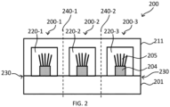
- a fluidic device 200 illustrated in Fig. 2 includes a substrate 201 having on its surface a plurality of microstructures 204 and nanowires 205 formed on the surfaces of the microstructures, and a cover 211 closely bonded to the substrate 201.
- the cover 211 has a plurality of flow channels or internal spaces 220-1, 220-2, and 220-3, and is bonded to the substrate 201 at a bonding surface surrounding them to form a close contact surface 230.
- the flow channels 220-1, 220-2, and 220-3 are formed so as to contain the respective microstructures 204 and nanowires 205.
- the fluidic device 200 illustrated in Fig. 2 has the plurality of flow channels 220-1, 220-2, and 220-3.
- the fluidic device 200 may be cut along boundaries 240-1 and 240-2 of the flow channels 220-1, 220-2, and 220-3. As a result, a plurality of individual fluidic devices 200-1, 200-2, and 200-3 may be fabricated.
- the cutting may include a blade or laser dicing process.
- a cover may be brought into close contact with each individual substrate to fabricate individual fluidic devices (not illustrated).
- a plurality of flow channels and/or fluidic devices may be fabricated from one substrate. The number may be other than three.
- the cover may have a plurality of internal spaces and a plurality of frames surrounding the respective internal spaces (not illustrated).
- a cover having a plurality of internal spaces may be brought into close contact with a plurality of target material pattern portions and/or microstructures, and the bonded component of the substrate and the cover may be cut or separated according to each internal space.
- flow channel typically refers to a space for accommodating a fluid.
- the flow channel may also be used interchangeably with terms, such as a fluid chamber and a fluid container.
- the flow channel may have an inlet for introducing a fluid thereinto and/or an outlet for discharging a fluid therefrom.
- the fluid may flow within the flow channel, or may be introduced into the flow channel and substantially stopped.
- a chaotic mixer chaos mixer
- a structure that causes a nonlinear and/or three-dimensional flow of the fluid flowing through the flow channel may be arranged in the flow channel.
- Such a structure may have, for example, a step in the flow channel, a change in cross-sectional area, or a change in the direction of the flow channel.
- a chaotic mixer having herringbone-shaped irregularities may be disposed on the inner wall surface of the flow channel (the surface of the substrate or the surface of the cover). These can promote the nonlinear flow of a fluid. As a result, for example, a larger amount of target substance in the solvent can be guided to the arranged microstructures (for example, nanowires) on the plurality of inner wall surfaces or the curved inner wall surfaces.
- the fluidic device may detect, measure, analyze, modify, process, and/or capture a substance contained in a fluid introduced into the flow channel.
- the fluidic device may have the nanowires.
- the fluidic device may use the nanowires to capture a substance contained in a fluid.
- the fluidic device may capture biomolecules in body fluids with the nanowires arranged in the flow channel.
- a fluid introduced into the flow channel may be a body fluid.
- body fluid refers to a body fluid obtained from a subject or a sample derived from the body fluid.
- the body fluid may be, but is not limited to, blood, serum, plasma, lymph fluid, tissue fluid such as interstitial fluid (interstitial fluid), intercellular fluid, body cavity fluid, serous cavity fluid, pleural fluid, ascites fluid, pericardial fluid, cerebrospinal fluid (spinal fluid), joint fluid (synovial fluid), and aqueous humor (aqueous humor).
- the body fluid may be a digestive fluid such as saliva, gastric fluid, bile, pancreatic fluid, or intestinal fluid, or may be sweat, tears, nasal fluid, urine, semen, vaginal fluid, amniotic fluid, or milk.
- the body fluid may be an animal body fluid or a human body fluid.
- the biomolecule may be an organelle or a vesicle.
- the vesicle may be, but is not limited to, a vacuole, a lysosome, a transport vesicle, a secretion, a gas vesicle, an extracellular matrix vesicle, an extracellular vesicle, or the like, and may include two or more thereof.
- the extracellular vesicle may be, but is not limited to, an exosome, an exotome, a shedding microvesicle, microvesicles, membrane particles, plasma membranes, pototic bullae, or the like.
- the vesicle may contain a nucleic acid.
- the biomolecule may be or may contain, but is not limited to, a cell.
- the cell may be a red blood cell, a white blood cell, an immune cell, or the like.
- the biomolecule may be a virus, a bacterium, or the like.
- the solution may be a body fluid or a liquid derived from a body fluid (such as a diluted liquid or a treated liquid).
- the solution may be a solution that is not a body fluid (derived from a non-body fluid), may be an artificially prepared liquid, or may be a mixture of a body fluid or a solution derived from a body fluid and a solution derived from a non-body fluid.
- the solution may be a solution used for sample measurement or may be a solution used for calibration measurement.
- the solution may be a standard solution or a calibration solution.
- the sample to be measured may be a specimen.
- the solution may contain a physiological buffer, such as phosphate buffered saline (PBS) or N-tris(hydroxymethyl)methyl-2-aminoethanesulfonic acid buffer (TES), containing the material to be recovered.
- PBS phosphate buffered saline
- TES N-tris(hydroxymethyl)methyl-2-aminoethanes
Landscapes
- Chemical & Material Sciences (AREA)
- Engineering & Computer Science (AREA)
- Chemical Kinetics & Catalysis (AREA)
- Organic Chemistry (AREA)
- Mechanical Engineering (AREA)
- Metallurgy (AREA)
- Materials Engineering (AREA)
- Health & Medical Sciences (AREA)
- General Health & Medical Sciences (AREA)
- Analytical Chemistry (AREA)
- Clinical Laboratory Science (AREA)
- Hematology (AREA)
- Dispersion Chemistry (AREA)
- Manufacturing & Machinery (AREA)
- Life Sciences & Earth Sciences (AREA)
- Microelectronics & Electronic Packaging (AREA)
- Molecular Biology (AREA)
- Physical Or Chemical Processes And Apparatus (AREA)
Applications Claiming Priority (2)
| Application Number | Priority Date | Filing Date | Title |
|---|---|---|---|
| JP2021131490 | 2021-08-11 | ||
| PCT/JP2022/030233 WO2023017801A1 (ja) | 2021-08-11 | 2022-08-08 | 基板をパターニングする方法、基板上に微細構造を形成する方法、及び流体デバイスを製造する方法。 |
Publications (2)
| Publication Number | Publication Date |
|---|---|
| EP4386484A1 true EP4386484A1 (de) | 2024-06-19 |
| EP4386484A4 EP4386484A4 (de) | 2025-08-27 |
Family
ID=85200616
Family Applications (1)
| Application Number | Title | Priority Date | Filing Date |
|---|---|---|---|
| EP22855863.1A Pending EP4386484A4 (de) | 2021-08-11 | 2022-08-08 | Verfahren zur strukturierung eines substrats, verfahren zur herstellung einer mikrostruktur auf einem substrat und verfahren zur herstellung einer fluidischen vorrichtung |
Country Status (5)
| Country | Link |
|---|---|
| US (1) | US12338523B2 (de) |
| EP (1) | EP4386484A4 (de) |
| JP (1) | JPWO2023017801A1 (de) |
| CN (1) | CN117813557A (de) |
| WO (1) | WO2023017801A1 (de) |
Families Citing this family (1)
| Publication number | Priority date | Publication date | Assignee | Title |
|---|---|---|---|---|
| WO2026042573A1 (ja) * | 2024-08-20 | 2026-02-26 | 東京エレクトロン株式会社 | 成膜方法、成膜装置およびメタルハードマスク |
Family Cites Families (9)
| Publication number | Priority date | Publication date | Assignee | Title |
|---|---|---|---|---|
| JPH0661160A (ja) * | 1992-08-07 | 1994-03-04 | Hitachi Ltd | パターン形成方法 |
| JP2000147792A (ja) * | 1998-11-13 | 2000-05-26 | Toyota Central Res & Dev Lab Inc | パターン形成方法 |
| JP2002169303A (ja) * | 2000-09-19 | 2002-06-14 | Toto Ltd | パターン形成方法、および、このパターン形成方法により製造された電子デバイス、光学素子、光触媒性部材 |
| US6969690B2 (en) * | 2003-03-21 | 2005-11-29 | The University Of North Carolina At Chapel Hill | Methods and apparatus for patterned deposition of nanostructure-containing materials by self-assembly and related articles |
| CN102760805B (zh) * | 2011-04-29 | 2015-03-11 | 清华大学 | 发光二极管 |
| JP2013182046A (ja) * | 2012-02-29 | 2013-09-12 | Nagoya Univ | 二次元パターニング方法およびマイクロ流路の製造方法 |
| JP6476990B2 (ja) * | 2014-06-05 | 2019-03-06 | 大日本印刷株式会社 | 印刷版、印刷版の製造方法、機能性素子の製造方法および印刷装置 |
| JP6640593B2 (ja) * | 2015-02-25 | 2020-02-05 | 学校法人神奈川大学 | 含フッ素組成物、パターン形成用基板、光分解性カップリング剤、パターン形成方法及びトランジスタの製造方法 |
| AU2017267653B2 (en) * | 2016-05-18 | 2021-05-13 | Illumina, Inc. | Self assembled patterning using patterned Hydrophobic surfaces |
-
2022
- 2022-08-08 JP JP2023541438A patent/JPWO2023017801A1/ja active Pending
- 2022-08-08 CN CN202280055856.1A patent/CN117813557A/zh active Pending
- 2022-08-08 US US18/682,253 patent/US12338523B2/en active Active
- 2022-08-08 EP EP22855863.1A patent/EP4386484A4/de active Pending
- 2022-08-08 WO PCT/JP2022/030233 patent/WO2023017801A1/ja not_active Ceased
Also Published As
| Publication number | Publication date |
|---|---|
| US12338523B2 (en) | 2025-06-24 |
| JPWO2023017801A1 (de) | 2023-02-16 |
| US20240376587A1 (en) | 2024-11-14 |
| CN117813557A (zh) | 2024-04-02 |
| WO2023017801A1 (ja) | 2023-02-16 |
| EP4386484A4 (de) | 2025-08-27 |
Similar Documents
| Publication | Publication Date | Title |
|---|---|---|
| US6743570B2 (en) | Method of using heat-depolymerizable polycarbonate sacrificial layer to create nano-fluidic devices | |
| KR20070053165A (ko) | 생화학적 분석을 위한 점적 조작용 장치, 상기 장치의 제조방법 및 마이크로 흐름 분석용 시스템 | |
| US7052616B2 (en) | Fabrication of molecular scale devices using fluidic assembly | |
| US8137569B2 (en) | Method of fabricating a membrane having a tapered pore | |
| EP2386865B1 (de) | Strömungskanalstruktur und herstellungsverfahren dafür | |
| JP6433430B2 (ja) | 三次元高表面領域電極の製造 | |
| KR101704901B1 (ko) | 전계효과 트랜지스터를 이용한 바이오 센서 및 이의 제조방법 | |
| EP4386484A1 (de) | Verfahren zur strukturierung eines substrats, verfahren zur herstellung einer mikrostruktur auf einem substrat und verfahren zur herstellung einer fluidischen vorrichtung | |
| US20030023149A1 (en) | Microfluidic microorganism detection system | |
| JP4248610B2 (ja) | 液体回路 | |
| US8847335B2 (en) | Membrane structure for electrochemical sensor | |
| JP2008039541A (ja) | マイクロ流路チップ及びそれを用いた生体高分子の処理方法 | |
| CN116544300A (zh) | 一种InAs/GaSb II类超晶格红外探测器的制备方法 | |
| JP2009521951A (ja) | 組み込まれたケイ素および細胞培養技術を用いて組み立てられたハイスループット細胞ベースアッセイ | |
| CN111868884B (zh) | SiC膜构造体 | |
| KR102587775B1 (ko) | 생물학적 응용들을 위한 독립 멤브레인을 생성하는 방법 | |
| US5001083A (en) | Method of priming semiconductor substrate for subsequent photoresist masking and etching | |
| TW201107260A (en) | Microprocessing of synthetic quartz glass substrate | |
| KR20180099243A (ko) | 나노포어 형성방법 | |
| CN102050427A (zh) | 纳流体测试器件的制备方法 | |
| JP2002252202A (ja) | 半導体基材表面への微細構造形成方法およびその方法により微細構造を形成した半導体基材ならびにそれを用いたデバイス | |
| CN112744782A (zh) | 一种微悬臂梁的制备方法 | |
| CN108193171B (zh) | 多通道集成滤光片光隔离结构的制造方法 | |
| JP2002357772A (ja) | 顕微鏡観察用プレート及びその製造方法 | |
| KR20210075286A (ko) | 나노 포어 필터 제조방법 및 이로부터 제조된 나노 포어 필터 |
Legal Events
| Date | Code | Title | Description |
|---|---|---|---|
| STAA | Information on the status of an ep patent application or granted ep patent |
Free format text: STATUS: THE INTERNATIONAL PUBLICATION HAS BEEN MADE |
|
| PUAI | Public reference made under article 153(3) epc to a published international application that has entered the european phase |
Free format text: ORIGINAL CODE: 0009012 |
|
| STAA | Information on the status of an ep patent application or granted ep patent |
Free format text: STATUS: REQUEST FOR EXAMINATION WAS MADE |
|
| 17P | Request for examination filed |
Effective date: 20240228 |
|
| AK | Designated contracting states |
Kind code of ref document: A1 Designated state(s): AL AT BE BG CH CY CZ DE DK EE ES FI FR GB GR HR HU IE IS IT LI LT LU LV MC MK MT NL NO PL PT RO RS SE SI SK SM TR |
|
| DAV | Request for validation of the european patent (deleted) | ||
| DAX | Request for extension of the european patent (deleted) | ||
| A4 | Supplementary search report drawn up and despatched |
Effective date: 20250730 |
|
| RIC1 | Information provided on ipc code assigned before grant |
Ipc: G03F 7/26 20060101AFI20250724BHEP Ipc: G03F 7/40 20060101ALI20250724BHEP Ipc: B01L 3/00 20060101ALI20250724BHEP Ipc: B81C 1/00 20060101ALI20250724BHEP Ipc: C23C 14/04 20060101ALI20250724BHEP |
|
| RAP3 | Party data changed (applicant data changed or rights of an application transferred) |
Owner name: CRAIF INC. |