EP4319513A1 - Circuit board structure and manufacturing method therefor - Google Patents
Circuit board structure and manufacturing method therefor Download PDFInfo
- Publication number
- EP4319513A1 EP4319513A1 EP22794243.0A EP22794243A EP4319513A1 EP 4319513 A1 EP4319513 A1 EP 4319513A1 EP 22794243 A EP22794243 A EP 22794243A EP 4319513 A1 EP4319513 A1 EP 4319513A1
- Authority
- EP
- European Patent Office
- Prior art keywords
- circuit board
- intercommunication
- hole
- laminated
- board arrangement
- Prior art date
- Legal status (The legal status is an assumption and is not a legal conclusion. Google has not performed a legal analysis and makes no representation as to the accuracy of the status listed.)
- Pending
Links
- 238000004519 manufacturing process Methods 0.000 title claims abstract description 50
- BQCADISMDOOEFD-UHFFFAOYSA-N Silver Chemical compound [Ag] BQCADISMDOOEFD-UHFFFAOYSA-N 0.000 claims abstract description 54
- 229910052709 silver Inorganic materials 0.000 claims abstract description 54
- 239000004332 silver Substances 0.000 claims abstract description 54
- 239000000853 adhesive Substances 0.000 claims abstract description 30
- 230000001070 adhesive effect Effects 0.000 claims abstract description 30
- 230000000149 penetrating effect Effects 0.000 claims abstract description 18
- 238000000034 method Methods 0.000 claims description 51
- 238000005429 filling process Methods 0.000 abstract description 11
- RYGMFSIKBFXOCR-UHFFFAOYSA-N Copper Chemical compound [Cu] RYGMFSIKBFXOCR-UHFFFAOYSA-N 0.000 abstract description 7
- 229910052802 copper Inorganic materials 0.000 abstract description 7
- 239000010949 copper Substances 0.000 abstract description 7
- 239000000463 material Substances 0.000 abstract description 7
- 239000010410 layer Substances 0.000 description 59
- 239000002390 adhesive tape Substances 0.000 description 7
- 238000007747 plating Methods 0.000 description 7
- 239000002356 single layer Substances 0.000 description 5
- 238000010276 construction Methods 0.000 description 3
- 230000000694 effects Effects 0.000 description 3
- 239000007788 liquid Substances 0.000 description 3
- 239000004593 Epoxy Substances 0.000 description 2
- 239000000919 ceramic Substances 0.000 description 2
- 238000003475 lamination Methods 0.000 description 2
- 239000007787 solid Substances 0.000 description 2
- 239000004925 Acrylic resin Substances 0.000 description 1
- 229920000178 Acrylic resin Polymers 0.000 description 1
- 239000004642 Polyimide Substances 0.000 description 1
- 230000009286 beneficial effect Effects 0.000 description 1
- 239000003795 chemical substances by application Substances 0.000 description 1
- 239000000428 dust Substances 0.000 description 1
- 239000003822 epoxy resin Substances 0.000 description 1
- 238000010030 laminating Methods 0.000 description 1
- 229920000647 polyepoxide Polymers 0.000 description 1
- 229920001721 polyimide Polymers 0.000 description 1
- 238000003825 pressing Methods 0.000 description 1
- 238000005096 rolling process Methods 0.000 description 1
- 238000005476 soldering Methods 0.000 description 1
- 238000006467 substitution reaction Methods 0.000 description 1
Images



Classifications
-
- H—ELECTRICITY
- H05—ELECTRIC TECHNIQUES NOT OTHERWISE PROVIDED FOR
- H05K—PRINTED CIRCUITS; CASINGS OR CONSTRUCTIONAL DETAILS OF ELECTRIC APPARATUS; MANUFACTURE OF ASSEMBLAGES OF ELECTRICAL COMPONENTS
- H05K3/00—Apparatus or processes for manufacturing printed circuits
- H05K3/46—Manufacturing multilayer circuits
- H05K3/4611—Manufacturing multilayer circuits by laminating two or more circuit boards
-
- H—ELECTRICITY
- H05—ELECTRIC TECHNIQUES NOT OTHERWISE PROVIDED FOR
- H05K—PRINTED CIRCUITS; CASINGS OR CONSTRUCTIONAL DETAILS OF ELECTRIC APPARATUS; MANUFACTURE OF ASSEMBLAGES OF ELECTRICAL COMPONENTS
- H05K3/00—Apparatus or processes for manufacturing printed circuits
- H05K3/40—Forming printed elements for providing electric connections to or between printed circuits
- H05K3/4038—Through-connections; Vertical interconnect access [VIA] connections
- H05K3/4053—Through-connections; Vertical interconnect access [VIA] connections by thick-film techniques
- H05K3/4069—Through-connections; Vertical interconnect access [VIA] connections by thick-film techniques for via connections in organic insulating substrates
-
- H—ELECTRICITY
- H05—ELECTRIC TECHNIQUES NOT OTHERWISE PROVIDED FOR
- H05K—PRINTED CIRCUITS; CASINGS OR CONSTRUCTIONAL DETAILS OF ELECTRIC APPARATUS; MANUFACTURE OF ASSEMBLAGES OF ELECTRICAL COMPONENTS
- H05K1/00—Printed circuits
- H05K1/02—Details
- H05K1/11—Printed elements for providing electric connections to or between printed circuits
- H05K1/115—Via connections; Lands around holes or via connections
-
- H—ELECTRICITY
- H05—ELECTRIC TECHNIQUES NOT OTHERWISE PROVIDED FOR
- H05K—PRINTED CIRCUITS; CASINGS OR CONSTRUCTIONAL DETAILS OF ELECTRIC APPARATUS; MANUFACTURE OF ASSEMBLAGES OF ELECTRICAL COMPONENTS
- H05K3/00—Apparatus or processes for manufacturing printed circuits
- H05K3/0094—Filling or covering plated through-holes or blind plated vias, e.g. for masking or for mechanical reinforcement
-
- H—ELECTRICITY
- H05—ELECTRIC TECHNIQUES NOT OTHERWISE PROVIDED FOR
- H05K—PRINTED CIRCUITS; CASINGS OR CONSTRUCTIONAL DETAILS OF ELECTRIC APPARATUS; MANUFACTURE OF ASSEMBLAGES OF ELECTRICAL COMPONENTS
- H05K3/00—Apparatus or processes for manufacturing printed circuits
- H05K3/40—Forming printed elements for providing electric connections to or between printed circuits
- H05K3/42—Plated through-holes or plated via connections
-
- H—ELECTRICITY
- H05—ELECTRIC TECHNIQUES NOT OTHERWISE PROVIDED FOR
- H05K—PRINTED CIRCUITS; CASINGS OR CONSTRUCTIONAL DETAILS OF ELECTRIC APPARATUS; MANUFACTURE OF ASSEMBLAGES OF ELECTRICAL COMPONENTS
- H05K3/00—Apparatus or processes for manufacturing printed circuits
- H05K3/46—Manufacturing multilayer circuits
- H05K3/4611—Manufacturing multilayer circuits by laminating two or more circuit boards
- H05K3/4614—Manufacturing multilayer circuits by laminating two or more circuit boards the electrical connections between the circuit boards being made during lamination
-
- H—ELECTRICITY
- H05—ELECTRIC TECHNIQUES NOT OTHERWISE PROVIDED FOR
- H05K—PRINTED CIRCUITS; CASINGS OR CONSTRUCTIONAL DETAILS OF ELECTRIC APPARATUS; MANUFACTURE OF ASSEMBLAGES OF ELECTRICAL COMPONENTS
- H05K2201/00—Indexing scheme relating to printed circuits covered by H05K1/00
- H05K2201/09—Shape and layout
- H05K2201/09209—Shape and layout details of conductors
- H05K2201/095—Conductive through-holes or vias
- H05K2201/096—Vertically aligned vias, holes or stacked vias
-
- H—ELECTRICITY
- H05—ELECTRIC TECHNIQUES NOT OTHERWISE PROVIDED FOR
- H05K—PRINTED CIRCUITS; CASINGS OR CONSTRUCTIONAL DETAILS OF ELECTRIC APPARATUS; MANUFACTURE OF ASSEMBLAGES OF ELECTRICAL COMPONENTS
- H05K3/00—Apparatus or processes for manufacturing printed circuits
- H05K3/40—Forming printed elements for providing electric connections to or between printed circuits
- H05K3/42—Plated through-holes or plated via connections
- H05K3/429—Plated through-holes specially for multilayer circuits, e.g. having connections to inner circuit layers
-
- H—ELECTRICITY
- H05—ELECTRIC TECHNIQUES NOT OTHERWISE PROVIDED FOR
- H05K—PRINTED CIRCUITS; CASINGS OR CONSTRUCTIONAL DETAILS OF ELECTRIC APPARATUS; MANUFACTURE OF ASSEMBLAGES OF ELECTRICAL COMPONENTS
- H05K3/00—Apparatus or processes for manufacturing printed circuits
- H05K3/46—Manufacturing multilayer circuits
- H05K3/4611—Manufacturing multilayer circuits by laminating two or more circuit boards
- H05K3/4623—Manufacturing multilayer circuits by laminating two or more circuit boards the circuit boards having internal via connections between two or more circuit layers before lamination, e.g. double-sided circuit boards
-
- H—ELECTRICITY
- H05—ELECTRIC TECHNIQUES NOT OTHERWISE PROVIDED FOR
- H05K—PRINTED CIRCUITS; CASINGS OR CONSTRUCTIONAL DETAILS OF ELECTRIC APPARATUS; MANUFACTURE OF ASSEMBLAGES OF ELECTRICAL COMPONENTS
- H05K3/00—Apparatus or processes for manufacturing printed circuits
- H05K3/46—Manufacturing multilayer circuits
- H05K3/4611—Manufacturing multilayer circuits by laminating two or more circuit boards
- H05K3/4638—Aligning and fixing the circuit boards before lamination; Detecting or measuring the misalignment after lamination; Aligning external circuit patterns or via connections relative to internal circuits
Definitions
- the present disclosure relates to the field of integrated circuits, and in particular, to a circuit board structure and a manufacturing method thereof.
- the manufacturing process of a conventional multi-layer circuit board structure includes alternately laminating multiple single-layer circuit boards and multiple prepregs according to a designed sequence of lamination, pressing them together in a high-temperature and high-pressure environment in cooperation with a traditional press, and then processing through holes that penetrate all single-layer circuit boards by means of electroless copper plating to form corresponding via holes to connect the multiple single-layer circuit boards to each other.
- circuit board structure and a manufacturing method thereof which are capable of effectively enlarging the number of laminatable circuit board layers and constructable structural thickness of the circuit board structure, and ensuring that a plurality of to-be-laminated circuit boards comprised in the circuit board structure are effectively conductive.
- the present disclosure provides a method for manufacturing a circuit board structure, the method comprising:
- the method further comprises the following:
- the method further comprises:
- the method further comprises:
- a correspondingly matched silver paste viscosity is smaller than 2.5P;
- the present disclosure provides a circuit board structure, the structure comprising a multilayer circuit board body, wherein the multilayer circuit board body is formed by stacking and bonding a plurality of to-be-laminated circuit boards to each other; At least one through hole penetrating the multilayer circuit board body is provided in a board surface of the multilayer circuit board body, and each through hole is filled with a viscosity-matched silver paste to form a corresponding via hole.
- the multilayer circuit board body comprises a top layer circuit board, a bottom layer circuit board, and at least one interconnection circuit board arrangement disposed between the top layer circuit board and the bottom layer circuit board, each interconnection circuit board arrangement comprising at least two to-be-laminated circuit boards stacked consecutively;
- the plurality of to-be-laminated circuit boards included in each interconnection circuit board arrangement are each provided with a first through hole having an overlapping projected position, and the plurality of first through holes corresponding to the interconnection circuit board arrangement are filled with a viscosity-matched silver paste to form a buried via hole for the interconnection circuit board arrangement.
- the multilayer circuit board body comprises at least one first intercommunication circuit board arrangement independent of a top layer circuit board, and each first intercommunication circuit board arrangement comprises a bottom layer circuit board and at least one to-be-laminated circuit board stacked with the bottom layer circuit board; At least one second through hole penetrating the first intercommunication circuit board arrangement is provided in a board surface of each first intercommunication circuit board arrangement, and each second through hole is filled with a viscosity-matched silver paste to form a first blind via hole for the first intercommunication circuit board arrangement.
- the multilayer circuit board body comprises at least one second intercommunication circuit board arrangement independent of a bottom layer circuit board, each second intercommunication circuit board arrangement comprising a top layer circuit board and at least one to-be-laminated circuit board stacked with the top layer circuit board;
- the plurality of to-be-laminated circuit boards included in each second intercommunication circuit board arrangement are each provided with a third through hole having an overlapping projected position, and the plurality of third through holes corresponding to the second intercommunication circuit board arrangement are filled with a viscosity-matched silver paste so as to form a second blind via hole for the second intercommunication circuit board arrangement.
- a correspondingly matched silver paste viscosity is smaller than 2.5P;
- the present disclosure forms a corresponding multilayer circuit board body by stacking a plurality of to-be-laminated circuit boards and bonding two adjacent to-be-laminated circuit boards with an adhesive medium that can be used in a room-temperature and low-pressure environment, so as to avoid the effects of a high-temperature and high-pressure environment on material properties, and to effectively enlarge the number of laminatable circuit board layers and constructable structural thickness of the circuit board structure.
- At least one through hole penetrating the multi-layer circuit board body is formed in a board surface of the multi-layer circuit board body, and each through hole is subjected to hole filling with a viscosity-matched silver paste to form a via hole corresponding to the through hole, so that the adhesive medium's failure of electroless copper plating can be solved through a silver paste filling process, and effective conduction of the plurality of to-be-laminated circuit boards included in the circuit board structure can be ensured.
- Reference numbers in the figures include: 100 - circuit board structure; 110 - to-be-laminated circuit board; 120 - multilayer circuit board body; 130 - through hole; 140 - via hole; 111 - top layer circuit board; 112 - bottom layer circuit board; 113 - interconnection circuit board arrangement; 114 - first through hole; 150 - buried via hole; 115 - first intercommunication circuit board arrangement; 116 - second through hole; 160 - first blind via hole; 117-second intercommunication circuit board arrangement; 118-third through hole; 170-second blind via hole.
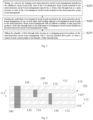
- FIG. 1 is a first schematic flowchart of a method for manufacturing a circuit board structure according to an embodiment of the present disclosure
- FIG. 2 is a schematic cross-sectional view of a circuit board structure 100 manufactured on the basis of the manufacturing method shown in FIG. 1
- the method for manufacturing a circuit board structure shown in FIG. 1 can effectively enlarge the number of laminatable circuit board layers and constructable structural thickness of the circuit board structure 100, and ensure that a plurality of to-be-laminated circuit boards 110 comprised in the circuit board structure 100 are efficiently conductive.
- the specific processes and steps of the method for manufacturing a circuit board structure shown in FIG. 1 are detailed as below.
- step S210 a plurality of to-be-laminated circuit boards are provided.
- the to-be-laminated circuit boards 110 may be single-layer circuit boards, or multilayer circuit boards that have been prepared, wherein the single-layer circuit boards may be, but are not limited to, any of common epoxy circuit boards, flexible circuit boards, ceramic circuit boards, etc., and the multilayer circuit boards may be formed by using any one or a combination of common epoxy circuit boards, flexible circuit boards, ceramic circuit boards, etc.
- the respective board surface sizes of the plurality of the to-be-laminated circuit boards 110 provided may be identical or completely different, and it is also possible that some of the to-be-laminated circuit boards 110 have a same board surface size.
- step S220 a plurality of to-be-laminated circuit boards are stacked, and an adhesive medium is used between two adjacent to-be-laminated circuit boards for bonding, so as to form a multilayer circuit board body.
- the plurality of to-be-laminated circuit boards 110 included in the multilayer circuit board body 120 are stacked on top of each other in a particular stacking order, and each to-be-laminated circuit board 110 is bonded to other adjacent to-be-laminated circuit boards 110by means of an adhesive medium.
- the adhesive medium typically has the characteristics of low fluidity, high bonding strength, bond ability at room temperature and normal pressure, and capability of withstanding high temperatures of reflow soldering after bonding, which can ensure that the lamination operations among the plurality of to-be-laminated circuit boards 110 is free from the influence of a high temperature and high pressure environment on the material properties, thereby enlarging the number of laminatable circuit board layers and constructable structural thickness of the circuit board structure 100.
- the adhesive medium may be, but is not limited to, an epoxy resin-based liquid adhesive, an acrylic resin-based liquid adhesive, a polyimide-based liquid adhesive, and a solid adhesive tape.
- a size-matched adhesive tape is die-cut in advance in accordance with the surface size of the to-be-laminated circuit boards 110, and then, in coordination with pins and a dedicated fixture for alignment of the adhesive tape, the adhesive tape with oneside of the release film removed is affixed on one side surface of oneto-be-laminated circuit board 110; then the release film on the other side of the adhesive tape is peeled off, and also with pins and a dedicated fixture for alignment, the other to-be-laminated circuit board 110 is stacked on and bonded to the previous to-be-laminated circuit board 110 through the adhesive tape.
- a rolling apparatus is used to ensure that the two to-be-laminated circuit boards 110 are bonded completely.
- the bonding operation of the circuit boards needs to be performed in a dust-free vacuum environment.
- a boring process is performed on a side board surface of the multilayer circuit board body to form at least one through hole penetrating the multilayer circuit board body.
- the multilayer circuit board body 120 may directly comprise a top layer circuit board 111, a bottom layer circuit board 112, and at least one to-be-laminated circuit board 110 located between the top layer circuit board 111 and the bottom layer circuit board 112.
- boring may be performed on a board surface of the top layer circuit board 111 away from the bottom layer circuit board 112, or on a board surface of the bottom layer circuit board 112 away from the top layer circuit board 111, thereby forming at least one through hole 130 in the multilayer circuit board body 120 that penetrates the multilayer circuit board body 120.
- a viscosity-matched silver paste is used to perform a hole filling process on the through hole, to form a via hole corresponding to the through hole.
- the multilayer circuit board body 120 can be fixed together with a hole filling fixture after removal of the adhesive residue in the hole, and then a viscosity-matched silver paste is selected according to an aspect ratio corresponding to the through hole 130 for hole filling from one side surface of the multilayer circuit board body 120, so as to fill the through hole 130 with the silver paste. Afterwards, upon complete standing, baking and curing is carried out to form a corresponding via hole 140.
- the aspect ratio of the through hole 130 is a ratio between the thickness of the corresponding multilayer circuit board body 120 and the diameter of the through hole 130.
- the present disclosure may, with reference to such principles that "a correspondingly matched silver paste viscosity is between 3.5P and 5.5P for an aspect ratio smaller than or equal to 8, between 2.5P and 3.5P for an aspect ratio greater than 8 and not more than 15, and smaller than 2.5P for an aspect ratio greater than 15", select a silver paste viscosity that matches the throughhole 130 to implement silver paste filling, so that the adhesive medium's failure of electroless copper plating can be solved through a silver paste filling process, and effective conduction of the plurality of to-be-laminated circuit boards 110 included in the circuit board structure 100 can be ensured.
- the silver paste in order to prevent the existence of voids in the silver paste in the hole, the silver paste needs to be stirred sufficiently before filling, and the silver paste filling process is carried out in a vacuum environment.
- the present disclosure can, through the execution of the above step S220, avoid the effects of a high-temperature and high-pressure environment on material properties, and effectively enlarge the number of laminatable circuit board layers and constructable structural thickness of the circuit board structure 100; and by executing the above step S240, the present disclosure solves the adhesive medium's failure of electroless copper plating through a silver paste filling process, thus achieving the effective plating of a high-aspect-ratio via hole and ensuring effective conduction of the plurality of to-be-laminated circuit boards 110 included in the circuit board structure 100.
- the present disclosure may also provide a circuit board structure manufacturing method for constructing a buried via hole structure during the forming process of a multilayer circuit board body. The specific processes and steps of this circuit board structure manufacturing method are described in detail as below.
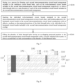
- FIG. 3 is a second schematic flowchart of a method for manufacturing a circuit board structure according to an embodiment of the present disclosure
- FIG. 4 is a schematic cross-sectional view of a circuit board structure 100 manufactured on the basis of the manufacturing method shown in FIG. 3
- the circuit board structure manufacturing method shown in FIG. 3 is used to construct a buried via hole 150 on the basis of the circuit board structure 100 shown in FIG. 2
- the circuit board structure manufacturing method shown in FIG. 3 is applied in the specific execution of step S220 shown in FIG. 1 .
- the plurality of to-be-laminated circuit boards 110 that are stacked, located between the top layer circuit board 111 and the bottom layer circuit board 112 and included in the multilayer circuit board body 120 in the circuit board structure 100 may correspondingly be divided into at least one interconnection circuit board arrangement 113, each interconnection circuit board arrangement 113 including at least two to-be-laminated circuit boards 110 stacked consecutively, and a same to-be-laminated circuit board 110 may be divided into different interconnection circuit board arrangements 113 (e.g., the third to-be-laminated circuit board 110 in FIG. 4 is divided into two interconnection circuit board arrangements 113 at the same time).
- a matching buried via hole 150 is constructed for each interconnection circuit board arrangement 113 based on the circuit board structure manufacturing method shown in FIG. 3 .
- the circuit board structure manufacturing method shown in FIG. 3 may include steps S250 to S270.
- step S250 during the forming process of each interconnection circuit board arrangement included in the multilayer circuit board body, a boring process is performed respectively on each to-be-laminated circuit board included in the interconnection circuit board arrangement to form a first through hole at a same location of each to-be-laminated circuit board included in the interconnection circuit board arrangement.
- each to-be-laminated circuit board 110 included in a same interconnection circuit board arrangement 113 has first through holes 114 formed at a plurality of board surface locations respectively, so as to form a plurality of through holes penetrating the interconnection circuit board arrangement 113 as the interconnection circuit board arrangement 113 is formed.
- step S260 the individual to-be-laminated circuit boards included in the interconnection circuit board arrangement are stacked on top of each other, and an adhesive medium is used to bond adjacent to-be-laminated circuit boards in the interconnection circuit board arrangement, so that the projected positions of the first through holes in the individual to-be-laminated circuit boards included in the interconnection circuit board arrangement overlap.
- the individual to-be-laminated circuit boards 110 included in the same interconnection circuit board arrangement 113 may be stacked on top of each other with direct reference to step S220, and an adhesive medium may be used to bond adjacent to-be-laminated circuit boards 110 in the interconnection circuit board arrangement 113, so that the projected positions of the first through holes 114 in the individual to-be-laminated circuit boards 110 included in the interconnection circuit board arrangement 113 overlap.
- a plurality of first through holes with an overlapping projected position in the interconnection circuit board arrangement are filled with a viscosity-matched silver paste to form a buried via hole corresponding to the plurality of first through holes.
- the plurality of first through holes 114 of the interconnection circuit board arrangement 113 that have an overlapping projected position may be directly regarded as one through hole all through the interconnection circuit board arrangement 113. Then a matching silver paste viscosity is selected according to the aspect ratio of the through hole running through the interconnection circuit board arrangement 113 to perform a silver paste filling process on the plurality of first through holes 114 with an overlapping projected position, thereby forming a buried via hole 150 corresponding to the interconnection circuit board arrangement 113, so as to intercommunicate the individual to-be-laminated circuit boards 110 included in the interconnection circuit board arrangement 113 through the buried via hole 150.
- the aspect ratio corresponding to the plurality of first through holes 114 with an overlapping projected position may be expressed as a ratio between the thickness of the board body of a corresponding interconnection circuit board arrangement 113 and the diameter of the first through holes 114.
- the present disclosure may ensure that the finally prepared circuit board structure 100 has buried via holes 150 that meet the engineer's buried via requirements by executing the above steps S250 to S270 during the execution of the above step S220, and at the same time, it can also ensure that the prepared buried via holes 150 are able to effectively conduct the plurality of intermediate to-be-laminated circuit boards 110 included in the circuit board structure 100.
- the present disclosure may also provide a circuit board structure manufacturing method for constructing a blind via hole structure during the forming process of a multilayer circuit board body. The specific processes and steps of this circuit board structure manufacturing method are described in detail as below.
- FIG. 5 is a third schematic flowchart of a method for manufacturing a circuit board structure according to an embodiment of the present disclosure
- FIG. 6 is a schematic cross-sectional view of a circuit board structure manufactured on the basis of the manufacturing method shown in FIG. 5
- the circuit board structure manufacturing method shown in FIG. 5 is used to construct a first blind hole 160 corresponding to the bottom layer circuit board 112 on the basis of the circuit board structure 100 shown in FIG. 2
- the circuit board structure manufacturing method shown in FIG. 5 is applied in the specific execution of step S220 shown in FIG. 1 .
- the other to-be-laminated circuit boards 110 than the top layer circuit board 111 that are included in the multilayer circuit board body 120 in the circuit board structure 100 may correspondingly be divided into at least one first intercommunication circuit board arrangement 115, such that each first intercommunication circuit board arrangement 115 includes a bottom layer circuit board 112 and at least one to-be-laminated circuit board 110 stacked to the bottom layer circuit board 112.
- a same to-be-laminated circuit board 110 may be divided into different first intercommunication circuit board arrangements 115 (e.g., the fifth to-be-laminated circuit board 110 in FIG. 6 is divided into two first intercommunication circuit board arrangements 115 at the same time).
- a matching first blind hole 160 is constructed for each of the first intercommunication circuit board arrangements 115 based on the circuit board manufacturing method shown in FIG. 5 .
- the circuit board manufacturing method shown in FIG. 5 may include steps S280, S290, and S310.
- step S280 in a process for forming each first intercommunication circuit board arrangement 115 included in the multilayer circuit board body 120, the individual to-be-laminated circuit boards 110 included in the first intercommunication circuit board arrangement 115 are stacked on top of each other, and adjacent to-be-laminated circuit boards in the first intercommunication circuit board arrangement are bonded with an adhesive medium, so as to obtain a to-be-treated circuit board arrangement.
- step S220 when it is necessary to construct and form a first interconnecting circuit board arrangement 115 during the construction of a multilayer circuit board body 120, reference may directly be made to step S220, whereby the individual to-be-laminated circuit boards 110 included in the first interconnecting circuit board arrangement 115 are stacked on top of each other, and adjacent to-be-laminated circuit boards 110 in the first intercommunication circuit board arrangement 115 are bonded with an adhesive medium, so as to obtain a to-be-treated circuit board arrangement.
- boring is performed on a side surface of the to-be-treated circuit board arrangement to form at least one second through hole penetrating the to-be-treated circuit board arrangement.
- At least one second through hole 116 penetrating the to-be-treated circuit board arrangement may be formed by boring a board surface of the to-be-treated circuit board arrangement corresponding to the first intercommunication circuit board arrangement 115 with reference to the above-stated step S230, where the aspect ratio of the second through hole 116 is a ratio between a board body thickness of the first intercommunication circuit board arrangement 115 and a dimeter of the second through hole 116.
- a viscosity-matched silver paste is used to perform a hole filling process on the second through hole, to form a first blind via hole corresponding to the second through hole in the first intercommunication circuit board arrangement.
- a matching silver paste viscosity may be selected according to the aspect ratio of the second through hole 116 to perform a silver paste filling process on each second through hole116, thereby forming a blind via hole 160 for the first intercommunication circuit board arrangement 115, so as to intercommunicate the individual to-be-laminated circuit boards 110 included in the first intercommunication circuit board arrangement 115 through the first blind via hole 160.
- the present disclosure may ensure that the finally prepared circuit board structure 100 has a first blind via hole 160 that meets the engineer's blind via requirements by executing the above steps S280 to S310 during the execution of the above step S220, and at the same time, it can also ensure that the prepared blind via hole 160 is able to effectively conduct the plurality of to-be-laminated circuit boards 110 at the bottom that are included in the circuit board structure 100.
- FIG. 7 is a fourth schematic flowchart of a method for manufacturing a circuit board structure according to an embodiment of the present disclosure
- FIG. 8 is a schematic cross-sectional view of a circuit board structure 100 manufactured on the basis of the manufacturing method shown in FIG. 7
- the circuit board structure manufacturing method shown in FIG. 7 is used to construct a second blind via hole 170 corresponding to the top layer circuit board 111 on the basis of the circuit board structure 100 shown in FIG. 2
- the circuit board structure manufacturing method shown in FIG. 7 is applied in the specific execution of the step S220 shown in FIG. 1 .
- the other to-be-laminated circuit boards 110 than the bottom layer circuit board 112 that are included in the multilayer circuit board body 120 in the circuit board structure 100 may correspondingly be divided into at least one second intercommunication circuit board arrangement 117, such that each second intercommunication circuit board arrangement 117 includes a top layer circuit board 111 and at least one to-be-laminated circuit board 110 stacked to the top layer circuit board 111.
- a same to-be-laminated circuit board 110 may be divided into different second intercommunication circuit board arrangements 117 (e.g., the second to-be-laminated circuit board 110 in FIG. 8 is divided into two second intercommunication circuit board arrangements 117 at the same time).
- a matching second blind via hole 170 is constructed for each of the second intercommunication circuit board arrangements 117 based on the circuit board manufacturing method shown in FIG. 7 .
- the circuit board manufacturing method shown in FIG. 7 may include steps S320 to S340.
- step S320 in a process for forming each second intercommunication circuit board arrangement included in the multilayer circuit board body, a boring process is performed respectively on each of to-be-laminated circuit boards included in the second intercommunication circuit board arrangement, so as to form a third through hole at a same location of each of the to-be-laminated circuit boards included in the second intercommunication circuit board arrangement.
- a boring process needs to be preferentially performed at a same board surface position of each to-be-laminated circuit board 110 included in the second intercommunication circuit board arrangement 117 respectively, so as to provide a third through hole 118 in each to-be-laminated circuit board 110 included in the second intercommunication circuit board arrangement 117.
- the respective projected positions of the third through holes 118 in all of the to-be-laminated circuit boards 110 included in a second intercommunication circuit board arrangement 117 overlap, such that when all of the to-be-laminated circuit boards 110 included in the second intercommunication circuit board arrangement 117 are stacked on top of each other, the plurality of the third through holes 118 with an overlapping projected position may be regarded as one through hole penetrating the second intercommunication circuit board arrangement 117.
- each to-be-laminated circuit board 110 included in a same second intercommunication circuit board arrangement 117 has third through holes 118 formed at a plurality of board surface locations respectively, so as to form a plurality of through holes penetrating the second intercommunication circuit board arrangement 117 as the second intercommunication circuit board arrangement 117 is formed.
- step S330 the individual to-be-laminated circuit boards included in the second intercommunication circuit board arrangement are stacked on top of each other, and an adhesive medium is used to bond adjacent to-be-laminated circuit boards in the second intercommunication circuit board arrangement, so that the projected positions of the third through holes in the individual to-be-laminated circuit boards included in the second intercommunication circuit board arrangement overlap.
- the individual to-be-laminated circuit boards 110 included in a same second intercommunication circuit board arrangement 117 may be stacked on top of each other with direct reference to step S220, and an adhesive medium may be used to bond adjacent to-be-laminated circuit boards 110 in the second intercommunication circuit board arrangement 117, so that the projected positions of the third through holes 118 in the individual to-be-laminated circuit boards 110 included in the second intercommunication circuit board arrangement 117 overlap.
- a plurality of third through holes with an overlapping projected position in the second intercommunication circuit board arrangement are filled with a viscosity-matched silver paste to form a second blind via hole corresponding to the plurality of third through holes.
- the plurality of third through holes 118 of the second intercommunication circuit board arrangement 117 that have an overlapping projected position may be directly regarded as one through hole all through the second intercommunication circuit board arrangement 117. Then a matching silver paste viscosity is selected according to the aspect ratio of the through hole running through the second intercommunication circuit board arrangement 117 to perform a silver paste filling process on the plurality of third through holes 118 with an overlapping projected position, thereby forming a second blind via hole 170 corresponding to the second intercommunication circuit board arrangement 117 so as to intercommunicate the individual to-be-laminated circuit boards 110 included in the second intercommunication circuit board arrangement 117 through the second blind via hole 170.
- the aspect ratio corresponding to the plurality of third through holes 118 with an overlapping projected position may be expressed as a ratio between the thickness of the board body of a corresponding second intercommunication circuit board arrangement 117 and the diameter of the third through holes 118.
- the present disclosure may ensure that the finally prepared circuit board structure 100 has blind via holes 170 that meet the engineer's blind via requirements by executing the above steps S250 to S270 during the execution of the above step S220, and at the same time, it can also ensure that the prepared blind via holes 170 are able to effectively conduct the plurality of to-be-laminated circuit boards 110 at the top that are included in the circuit board structure 100.
- any one or a combination of the circuit board structure manufacturing methods shown in FIGS. 3 , 5 , and 7 provided in the present disclosure may be selected by an engineer according to his or her own needs during the execution of the circuit board structure manufacturing method shown in FIG. 1 , so as to ensure that the finally prepared circuit board structure 100 is able to efficiently enlarge the number of laminatable circuit board layers and constructable structural thickness and that a plurality of to-be-laminated circuit boards 110 comprised in the circuit board structure 100 are efficiently conductive while correspondingly meeting the engineer's needs for buried/blind via holes.
- the circuit board structure 100 shown in FIG. 9 is a device structure prepared by simultaneously adopting the circuit board structure manufacturing methods illustrated in FIGS. 1 , 3 , 5 , and 7 , and the fifth to-be-laminated circuit board 110 in FIG. 9 may serve as both a part of the interconnection circuit board arrangement 113 and a part of the first intercommunication circuit board arrangement 115.
- a corresponding multilayer circuit board body is formed by stacking a plurality of to-be-laminated circuit boards and bonding two adjacent to-be-laminated circuit boards with an adhesive medium that can be used in a room-temperature and low-pressure environment, so as to avoid the effects of a high-temperature and high-pressure environment on material properties, and to effectively enlarge the number of laminatable circuit board layers and constructable structural thickness of the circuit board structure.
- At least one through hole penetrating the multi-layer circuit board body is formed in a board surface of the multi-layer circuit board body, and each through hole is subjected to hole filling with a viscosity-matched silver paste to form a via hole corresponding to the through hole, so that the adhesive medium's failure of electroless copper plating can be solved through a silver paste filling process, and effective conduction of the plurality of to-be-laminated circuit boards included in the circuit board structure can be ensured.
Landscapes
- Engineering & Computer Science (AREA)
- Microelectronics & Electronic Packaging (AREA)
- Manufacturing & Machinery (AREA)
- Production Of Multi-Layered Print Wiring Board (AREA)
Abstract
Description
- The present disclosure relates to the field of integrated circuits, and in particular, to a circuit board structure and a manufacturing method thereof.
- The manufacturing process of a conventional multi-layer circuit board structure includes alternately laminating multiple single-layer circuit boards and multiple prepregs according to a designed sequence of lamination, pressing them together in a high-temperature and high-pressure environment in cooperation with a traditional press, and then processing through holes that penetrate all single-layer circuit boards by means of electroless copper plating to form corresponding via holes to connect the multiple single-layer circuit boards to each other. It should be noted that such a manufacturing process will lead to material performance failure in case of too many times of press, due to the fact that the materials themselves typically have heat-resistant and pressure-resistant limits, and will cause failure to effectively convert through holes with a too large depth into via holes due to the limited throw power of an agent used for electroless copper plating, so that the number of circuit board layers and the thickness of the prepared multi-layer circuit board structure are obviously not large.
- In view of the above, it is an object of the present disclosure to provide a circuit board structure and a manufacturing method thereof, which are capable of effectively enlarging the number of laminatable circuit board layers and constructable structural thickness of the circuit board structure, and ensuring that a plurality of to-be-laminated circuit boards comprised in the circuit board structure are effectively conductive.
- I In order to achieve the object above, the technical solutions employed in the embodiments of the present disclosure are as follows.
- According to a first aspect, the present disclosure provides a method for manufacturing a circuit board structure, the method comprising:
- Providing a plurality of to-be-laminated circuit boards;
- Stacking the plurality of to-be-laminated circuit boards, and performing bonding between two adjacent to-be-laminated circuit boards with an adhesive medium to form a multi-layer circuit board body;
- Boring a side surface of the multilayer circuit board body to form at least one through hole penetrating the multilayer circuit board body;
- Filling each through hole with a viscosity-matched silver paste to form a via hole corresponding to the through hole.
- In an optional implementation, if the multilayer circuit board body comprises at least one interconnection circuit board arrangement disposed between a top layer circuit board and a bottom layer circuit board, each interconnection circuit board arrangement comprising at least two to-be-laminated circuit boards stacked consecutively, the method further comprises the following:
- Ina process for forming each interconnection circuit board arrangement included in the multilayer circuit board body, boring each of the to-be-laminated circuit boards included in the interconnection circuit board arrangement respectively to form a first through hole at a same location of each of the to-be-laminated circuit boards included in the interconnection circuit board arrangement;
- Stacking the individual to-be-laminated circuit boards included in the interconnection circuit board arrangement on top of each other, and bonding adjacent to-be-laminated circuit boards in the interconnection circuit board arrangement with an adhesive medium so that projected positions of the first through holes in the individual to-be-laminated circuit boards included in the interconnection circuit board arrangement overlap;
- Filling the plurality of first through holes having an overlapping projected position in the interconnection circuit board arrangement with a viscosity-matched silver paste, to form a buried via hole corresponding to the plurality of first through holes, wherein the buried via hole is used to intercommunicate the individual to-be-laminated circuit boards included in the interconnection circuit board arrangement.
- In an optional implementation, if the multilayer circuit board body comprises at least one first intercommunication circuit board arrangement independent of a top layer circuit board, each first intercommunication circuit board arrangement comprising a bottom layer circuit board and at least one to-be-laminated circuit board stacked with the bottom layer circuit board, the method further comprises:
- In a process for forming each first intercommunication circuit board arrangement included in the multilayer circuit board body, stacking the individual to-be-laminated circuit boards included in the first intercommunication circuit board arrangement on top of each other, and bonding adjacent to-be-laminated circuit boards in the first intercommunication circuit board arrangement with an adhesive medium, to obtain a to-be-treated circuit board arrangement;
- Boring a side surface of the to-be-treated circuit board arrangement to form at least one second through hole penetrating the to-be-treated circuit board arrangement;
- Filling each second through hole with a viscosity-matched silver paste, to form a first blind via hole corresponding to the second through hole in the first intercommunication circuit board arrangement, wherein the first blind via hole is used to intercommunicate the individual to-be-laminated circuit boards included in the first intercommunication circuit board arrangement.
- In an optional implementation, if the multilayer circuit board body comprises at least one second intercommunication circuit board arrangement independent of a bottom layer circuit board, each second intercommunication circuit board arrangement comprising a top layer circuit board and at least one to-be-laminated circuit board stacked with the top layer circuit board, the method further comprises:
- In a process for forming each second intercommunication circuit board arrangement included in the multilayer circuit board body, boring each of the to-be-laminated circuit boards included in the second intercommunication circuit board arrangement respectively to form a third through hole at a same location of each of the to-be-laminated circuit boards included in the second intercommunication circuit board arrangement;
- Stacking the individual to-be-laminated circuit boards included in the second intercommunication circuit board arrangement on top of each other, and bonding adjacent to-be-laminated circuit boards in the second intercommunication circuit board arrangement with an adhesive medium so that projected positions of the third through holes in the individual to-be-laminated circuit boards included in the second intercommunication circuit board arrangement overlap;
- Filling the plurality of third through holes having an overlapping projected position in the second intercommunication circuit board arrangement with a viscosity-matched silver paste, to form a second blind via hole corresponding to the plurality of third through holes, wherein the second blind via hole is used to intercommunicate the individual to-be-laminated circuit boards included in the second intercommunication circuit board arrangement.
- In an optional implementation, for a through hole with an aspect ratio greater than 15, a correspondingly matched silver paste viscosity is smaller than 2.5P;
- For a through hole with an aspect ratio greater than 8 and not more than 15, a correspondingly matched silver paste viscosity is between 2.5P and 3.5P;
- For a through hole with an aspect ratio of smaller than or equal to 8, a correspondingly matched silver paste viscosity is between 3.5P and 5.5P.
- According to a second aspect, the present disclosure provides a circuit board structure, the structure comprising a multilayer circuit board body, wherein the multilayer circuit board body is formed by stacking and bonding a plurality of to-be-laminated circuit boards to each other;
At least one through hole penetrating the multilayer circuit board body is provided in a board surface of the multilayer circuit board body, and each through hole is filled with a viscosity-matched silver paste to form a corresponding via hole. - In an optional implementation, the multilayer circuit board body comprises a top layer circuit board, a bottom layer circuit board, and at least one interconnection circuit board arrangement disposed between the top layer circuit board and the bottom layer circuit board, each interconnection circuit board arrangement comprising at least two to-be-laminated circuit boards stacked consecutively;
The plurality of to-be-laminated circuit boards included in each interconnection circuit board arrangement are each provided with a first through hole having an overlapping projected position, and the plurality of first through holes corresponding to the interconnection circuit board arrangement are filled with a viscosity-matched silver paste to form a buried via hole for the interconnection circuit board arrangement. - In an optional implementation, the multilayer circuit board body comprises at least one first intercommunication circuit board arrangement independent of a top layer circuit board, and each first intercommunication circuit board arrangement comprises a bottom layer circuit board and at least one to-be-laminated circuit board stacked with the bottom layer circuit board;
At least one second through hole penetrating the first intercommunication circuit board arrangement is provided in a board surface of each first intercommunication circuit board arrangement, and each second through hole is filled with a viscosity-matched silver paste to form a first blind via hole for the first intercommunication circuit board arrangement. - In an optional implementation, the multilayer circuit board body comprises at least one second intercommunication circuit board arrangement independent of a bottom layer circuit board, each second intercommunication circuit board arrangement comprising a top layer circuit board and at least one to-be-laminated circuit board stacked with the top layer circuit board;
The plurality of to-be-laminated circuit boards included in each second intercommunication circuit board arrangement are each provided with a third through hole having an overlapping projected position, and the plurality of third through holes corresponding to the second intercommunication circuit board arrangement are filled with a viscosity-matched silver paste so as to form a second blind via hole for the second intercommunication circuit board arrangement. - In an optional implementation, for a through hole with an aspect ratio greater than 15, a correspondingly matched silver paste viscosity is smaller than 2.5P;
- For a through hole with an aspect ratio greater than 8 and not more than 15, a correspondingly matched silver paste viscosity is between 2.5P and 3.5P;
- For a through hole with an aspect ratio of smaller than or equal to 8, a correspondingly matched silver paste viscosity is between 3.5P and 5.5P.
- In this context, the beneficial effects of the embodiments of the present disclosure include the following.
- The present disclosure forms a corresponding multilayer circuit board body by stacking a plurality of to-be-laminated circuit boards and bonding two adjacent to-be-laminated circuit boards with an adhesive medium that can be used in a room-temperature and low-pressure environment, so as to avoid the effects of a high-temperature and high-pressure environment on material properties, and to effectively enlarge the number of laminatable circuit board layers and constructable structural thickness of the circuit board structure. Afterwards, at least one through hole penetrating the multi-layer circuit board body is formed in a board surface of the multi-layer circuit board body, and each through hole is subjected to hole filling with a viscosity-matched silver paste to form a via hole corresponding to the through hole, so that the adhesive medium's failure of electroless copper plating can be solved through a silver paste filling process, and effective conduction of the plurality of to-be-laminated circuit boards included in the circuit board structure can be ensured.
- In order to make the above objects, features and advantages of the present disclosure more apparent, preferred embodiments are exemplified below, and are described in detail as follows in conjunction with the accompanying drawings.
- In order to more clearly illustrate the technical solutions of the embodiments of the present disclosure, the accompanying drawings to be used in the embodiments will be briefly introduced below. It should be understood that the following figures are only illustrative of certain embodiments of the present disclosure, and therefore should not be regarded as limiting to its scope. For those skilled in the art, other related drawings could also be obtained from these drawings without exercise of any ingenuity.
-
FIG. 1 is a first schematic flowchart of a method for manufacturing a circuit board structure according to an embodiment of the present disclosure; -
FIG. 2 is a schematic cross-sectional view of a circuit board structure manufactured on the basis of the manufacturing method shown inFIG. 1 ; -
FIG. 3 is a second schematic flowchart of a method for manufacturing a circuit board structure according to an embodiment of the present disclosure; -
FIG. 4 is a schematic cross-sectional view of a circuit board structure manufactured on the basis of the manufacturing method shown inFIG. 3 ; -
FIG. 5 is a third schematic flowchart of a method for manufacturing a circuit board structure according to an embodiment of the present disclosure; -
FIG. 6 is a schematic cross-sectional view of a circuit board structure manufactured on the basis of the manufacturing method shown inFIG. 5 ; -
FIG. 7 is a fourth schematic flowchart of a method for manufacturing a circuit board structure according to an embodiment of the present disclosure; -
FIG. 8 is a schematic cross-sectional view of a circuit board structure manufactured on the basis of the manufacturing method shown inFIG. 7 ; and -
FIG. 9 is a schematic cross-sectional view of a circuit board structure manufactured on the basis of the manufacturing methods shown inFIGS. 1 ,3 ,5 , and7 . - Reference numbers in the figures include: 100 - circuit board structure; 110 - to-be-laminated circuit board; 120 - multilayer circuit board body; 130 - through hole; 140 - via hole; 111 - top layer circuit board; 112 - bottom layer circuit board; 113 - interconnection circuit board arrangement; 114 - first through hole; 150 - buried via hole; 115 - first intercommunication circuit board arrangement; 116 - second through hole; 160 - first blind via hole; 117-second intercommunication circuit board arrangement; 118-third through hole; 170-second blind via hole.
- In order to make the objects, technical solutions and advantages of the embodiments of the present disclosure clearer, the technical solutions in the embodiments of the present disclosure will be clearly and completely described below in conjunction with the accompanying drawings. Apparently, the embodiments described herein are some, but not all, embodiments of the present disclosure. The components in the embodiments of the present disclosure described and illustrated herein may generally be arranged and designed in a variety of different configurations.
- Accordingly, the following detailed description of the embodiments of the present disclosure as provided in the accompanying drawings is not intended to limit the scope of the present disclosure, but merely to indicate selected embodiments of the present disclosure. Based on the embodiments in the present disclosure, all other embodiments obtained without exercise of ingenuity by a person of ordinary skill in the art fall within the scope of protection of the present disclosure.
- It should be noted that like reference numerals and letters refer to like items in the following figures, and thus, once an item is defined in one figure, it need not be further defined and explained in subsequent ones.
- In the description of the present disclosure, it should be noted that an orientation or a positional relationship indicated by such terms as "upper", "lower", "inner" and "outer", if any, is based on that shown in the drawings, or that of the product of the present disclosure as it is in use. This is only for ease and simplicity of description, without indicating or implying that the device or the element referred to must have a specific orientation, or be constructed and operated in a particular orientation, and thus it should not be construed as limiting to the present disclosure.
- It is to be noted that relational terms such as "first" and "second" herein are used only to distinguish one entity or operation from another, and do not necessarily require or imply any such actual relationship or order between those entities or operations. Furthermore, the terms "including", "comprising", or any other variant thereof, are intended to cover non-exclusive inclusion, such that a process, method, article, or apparatus comprising a set of elements includes not only those elements, but also other elements not expressly listed, or elements that are inherent to such process, method, article or apparatus. Without further limitation, the fact that an element is defined by the phrase "comprising a ......" does not preclude the existence of additional identical elements in the process, method, article or apparatus that comprises the element. For a person of ordinary skill in the art, the specific meanings of these terms in the present disclosure may be understood in specific contexts.
- Some embodiments of the present disclosure are described in detail below in conjunction with the accompanying drawings. The following embodiments and features therein may be combined with each other in the absence of conflicts.
- Referring to
FIGS. 1 and 2 in combination,FIG. 1 is a first schematic flowchart of a method for manufacturing a circuit board structure according to an embodiment of the present disclosure, andFIG. 2 is a schematic cross-sectional view of acircuit board structure 100 manufactured on the basis of the manufacturing method shown inFIG. 1 . In the embodiment of the present disclosure, the method for manufacturing a circuit board structure shown inFIG. 1 can effectively enlarge the number of laminatable circuit board layers and constructable structural thickness of thecircuit board structure 100, and ensure that a plurality of to-be-laminated circuit boards 110 comprised in thecircuit board structure 100 are efficiently conductive. The specific processes and steps of the method for manufacturing a circuit board structure shown inFIG. 1 are detailed as below. - At step S210, a plurality of to-be-laminated circuit boards are provided.
- In this embodiment, the to-
be-laminated circuit boards 110 may be single-layer circuit boards, or multilayer circuit boards that have been prepared, wherein the single-layer circuit boards may be, but are not limited to, any of common epoxy circuit boards, flexible circuit boards, ceramic circuit boards, etc., and the multilayer circuit boards may be formed by using any one or a combination of common epoxy circuit boards, flexible circuit boards, ceramic circuit boards, etc. In addition, the respective board surface sizes of the plurality of the to-be-laminated circuit boards 110 provided may be identical or completely different, and it is also possible that some of the to-be-laminated circuit boards 110 have a same board surface size. - At step S220, a plurality of to-be-laminated circuit boards are stacked, and an adhesive medium is used between two adjacent to-be-laminated circuit boards for bonding, so as to form a multilayer circuit board body.
- In this embodiment, the plurality of to-
be-laminated circuit boards 110 included in the multilayercircuit board body 120 are stacked on top of each other in a particular stacking order, and each to-be-laminated circuit board 110 is bonded to other adjacent to-be-laminated circuit boards 110by means of an adhesive medium. The adhesive medium typically has the characteristics of low fluidity, high bonding strength, bond ability at room temperature and normal pressure, and capability of withstanding high temperatures of reflow soldering after bonding, which can ensure that the lamination operations among the plurality of to-be-laminated circuit boards 110 is free from the influence of a high temperature and high pressure environment on the material properties, thereby enlarging the number of laminatable circuit board layers and constructable structural thickness of thecircuit board structure 100. The adhesive medium may be, but is not limited to, an epoxy resin-based liquid adhesive, an acrylic resin-based liquid adhesive, a polyimide-based liquid adhesive, and a solid adhesive tape. - In one implementation of this embodiment, ifa solid adhesive tape is used as the adhesive medium, when bonding two to-
be-laminated circuit boards 110 that are stacked up, a size-matched adhesive tape is die-cut in advance in accordance with the surface size of the to-be-laminated circuit boards 110, and then, in coordination with pins and a dedicated fixture for alignment of the adhesive tape, the adhesive tape with oneside of the release film removed is affixed on one side surface of oneto-be-laminated circuit board 110; then the release film on the other side of the adhesive tape is peeled off, and also with pins and a dedicated fixture for alignment, the other to-be-laminated circuit board 110 is stacked on and bonded to the previous to-be-laminated circuit board 110 through the adhesive tape. Thereafter, a rolling apparatus is used to ensure that the two to-be-laminated circuit boards 110 are bonded completely. In this process, in order to avoid the generation of bubbles and/or dust mixing, the bonding operation of the circuit boards needs to be performed in a dust-free vacuum environment. - At step S230, a boring process is performed on a side board surface of the multilayer circuit board body to form at least one through hole penetrating the multilayer circuit board body.
- In this embodiment, after the multilayer
circuit board body 120 is formed by performing the step S220, the multilayercircuit board body 120 may directly comprise a toplayer circuit board 111, a bottomlayer circuit board 112, and at least one to-be-laminated circuit board 110 located between the toplayer circuit board 111 and the bottomlayer circuit board 112. At this point, boring may be performed on a board surface of the toplayer circuit board 111 away from the bottomlayer circuit board 112, or on a board surface of the bottomlayer circuit board 112 away from the toplayer circuit board 111, thereby forming at least one throughhole 130 in the multilayercircuit board body 120 that penetrates the multilayercircuit board body 120. - At step S240, for each through hole, a viscosity-matched silver paste is used to perform a hole filling process on the through hole, to form a via hole corresponding to the through hole.
- In this embodiment, after a through
hole 130 is constructed, the multilayercircuit board body 120 can be fixed together with a hole filling fixture after removal of the adhesive residue in the hole, and then a viscosity-matched silver paste is selected according to an aspect ratio corresponding to the throughhole 130 for hole filling from one side surface of the multilayercircuit board body 120, so as to fill the throughhole 130 with the silver paste. Afterwards, upon complete standing, baking and curing is carried out to form a corresponding viahole 140. The aspect ratio of the throughhole 130 is a ratio between the thickness of the corresponding multilayercircuit board body 120 and the diameter of the throughhole 130. The present disclosure may, with reference to such principles that "a correspondingly matched silver paste viscosity is between 3.5P and 5.5P for an aspect ratio smaller than or equal to 8, between 2.5P and 3.5P for an aspect ratio greater than 8 and not more than 15, and smaller than 2.5P for an aspect ratio greater than 15", select a silver paste viscosity that matches thethroughhole 130 to implement silver paste filling, so that the adhesive medium's failure of electroless copper plating can be solved through a silver paste filling process, and effective conduction of the plurality of to-be-laminated circuit boards 110 included in thecircuit board structure 100 can be ensured. - In one implementation of the present embodiment, in order to prevent the existence of voids in the silver paste in the hole, the silver paste needs to be stirred sufficiently before filling, and the silver paste filling process is carried out in a vacuum environment.
- As a result, the present disclosure can, through the execution of the above step S220, avoid the effects of a high-temperature and high-pressure environment on material properties, and effectively enlarge the number of laminatable circuit board layers and constructable structural thickness of the
circuit board structure 100; and by executing the above step S240, the present disclosure solves the adhesive medium's failure of electroless copper plating through a silver paste filling process, thus achieving the effective plating of a high-aspect-ratio via hole and ensuring effective conduction of the plurality of to-be-laminated circuit boards 110 included in thecircuit board structure 100. - In the present disclosure, if the engineer has needs for a buried via hole in the
circuit board structure 100 to be constructed, it is necessary that the number of to-be-laminated circuit boards 110 between the corresponding toplayer circuit board 111 and the bottomlayer circuit board 112 be designed to be multiple, and a buried via hole structure satisfying the buried via hole requirements be constructed in the foregoing forming process of the multi-layer circuit board body. To this end, the present disclosure may also provide a circuit board structure manufacturing method for constructing a buried via hole structure during the forming process of a multilayer circuit board body. The specific processes and steps of this circuit board structure manufacturing method are described in detail as below. - Referring to
FIGS. 3 and 4 in combination,FIG. 3 is a second schematic flowchart of a method for manufacturing a circuit board structure according to an embodiment of the present disclosure, andFIG. 4 is a schematic cross-sectional view of acircuit board structure 100 manufactured on the basis of the manufacturing method shown inFIG. 3 . In this embodiment of the present disclosure, the circuit board structure manufacturing method shown inFIG. 3 is used to construct a buried viahole 150 on the basis of thecircuit board structure 100 shown inFIG. 2 , and the circuit board structure manufacturing method shown inFIG. 3 is applied in the specific execution of step S220 shown inFIG. 1 . - In the
circuit board structure 100 manufactured based on the manufacturing method shown inFIG. 3 , the plurality of to-be-laminated circuit boards 110that are stacked, located between the toplayer circuit board 111 and the bottomlayer circuit board 112 and included in the multilayercircuit board body 120 in thecircuit board structure 100 may correspondingly be divided into at least one interconnectioncircuit board arrangement 113, each interconnectioncircuit board arrangement 113 including at least two to-be-laminated circuit boards 110 stacked consecutively, and a same to-be-laminated circuit board 110 may be divided into different interconnection circuit board arrangements 113 (e.g., the third to-be-laminated circuit board 110 inFIG. 4 is divided into two interconnectioncircuit board arrangements 113 at the same time). And then, a matching buried viahole 150 is constructed for each interconnectioncircuit board arrangement 113 based on the circuit board structure manufacturing method shown inFIG. 3 . In this case, the circuit board structure manufacturing method shown inFIG. 3 may include steps S250 to S270. - At step S250, during the forming process of each interconnection circuit board arrangement included in the multilayer circuit board body, a boring process is performed respectively on each to-be-laminated circuit board included in the interconnection circuit board arrangement to form a first through hole at a same location of each to-be-laminated circuit board included in the interconnection circuit board arrangement.
- In this embodiment, when an interconnection
circuit board arrangement 113 needs to be constructed and formed during the construction of the multilayercircuit board body 120, a boring process needs to be preferentially performed at a same board surface position of each to-be-laminated circuit board 110 included in the interconnectioncircuit board arrangement 113 respectively, so as to provide a first throughhole 114 in each to-be-laminated circuit board 110 included in the interconnectioncircuit board arrangement 113. The respective projected positions of the first throughholes 114 in all of the to-be-laminated circuit boards 110 included in a same interconnectioncircuit board arrangement 113 overlap, such that when all of the to-be-laminated circuit boards 110 included in the interconnectioncircuit board arrangement 113 are stacked on top of each other, the plurality of the first throughholes 114 with an overlapping projected position may be regarded as one through hole penetrating the interconnectioncircuit board arrangement 113. - In one implementation of this embodiment, each to-
be-laminated circuit board 110 included in a same interconnectioncircuit board arrangement 113 has first throughholes 114 formed at a plurality of board surface locations respectively, so as to form a plurality of through holes penetrating the interconnectioncircuit board arrangement 113 as the interconnectioncircuit board arrangement 113 is formed. - At step S260, the individual to-be-laminated circuit boards included in the interconnection circuit board arrangement are stacked on top of each other, and an adhesive medium is used to bond adjacent to-be-laminated circuit boards in the interconnection circuit board arrangement, so that the projected positions of the first through holes in the individual to-be-laminated circuit boards included in the interconnection circuit board arrangement overlap.
- In this embodiment, after corresponding first through
holes 114 are constructed ineach of the to-be-laminated circuit boards 110 included in a same interconnectioncircuit board arrangement 113, the individual to-be-laminated circuit boards 110 included in the same interconnectioncircuit board arrangement 113 may be stacked on top of each other with direct reference to step S220, and an adhesive medium may be used to bond adjacent to-be-laminated circuit boards 110 in the interconnectioncircuit board arrangement 113, so that the projected positions of the first throughholes 114 in the individual to-be-laminated circuit boards 110 included in the interconnectioncircuit board arrangement 113 overlap. - At step S270, a plurality of first through holes with an overlapping projected position in the interconnection circuit board arrangement are filled with a viscosity-matched silver paste to form a buried via hole corresponding to the plurality of first through holes.
- In this embodiment, upon completion of the bonding operation of the interconnection
circuit board arrangement 113, the plurality of first throughholes 114 of the interconnectioncircuit board arrangement 113 that have an overlapping projected position may be directly regarded as one through hole all through the interconnectioncircuit board arrangement 113. Then a matching silver paste viscosity is selected according to the aspect ratio of the through hole running through the interconnectioncircuit board arrangement 113 to perform a silver paste filling process on the plurality of first throughholes 114 with an overlapping projected position, thereby forming a buried viahole 150 corresponding to the interconnectioncircuit board arrangement 113, so as to intercommunicate the individual to-be-laminated circuit boards 110 included in the interconnectioncircuit board arrangement 113 through the buried viahole 150. The aspect ratio corresponding to the plurality of first throughholes 114 with an overlapping projected position may be expressed as a ratio between the thickness of the board body of a corresponding interconnectioncircuit board arrangement 113 and the diameter of the first throughholes 114. - As a result, the present disclosure may ensure that the finally prepared
circuit board structure 100 has buried viaholes 150 that meet the engineer's buried via requirements by executing the above steps S250 to S270 during the execution of the above step S220, and at the same time, it can also ensure that the prepared buried viaholes 150 are able to effectively conduct the plurality of intermediate to-be-laminated circuit boards 110 included in thecircuit board structure 100. - In the present disclosure, if the engineer has needs for a blind via hole in the
circuit board structure 100 to be constructed, it is necessary that the number of to-be-laminated circuit boards 110 between the corresponding toplayer circuit board 111 and the bottomlayer circuit board 112 be designed to be multiple, and a blind via hole structure satisfying the blind via requirements be constructed in the foregoing forming process of the multi-layer circuit board body. To this end, the present disclosure may also provide a circuit board structure manufacturing method for constructing a blind via hole structure during the forming process of a multilayer circuit board body. The specific processes and steps of this circuit board structure manufacturing method are described in detail as below. - Optionally, referring to
FIGS. 5 and 6 in combination,FIG. 5 is a third schematic flowchart of a method for manufacturing a circuit board structure according to an embodiment of the present disclosure, andFIG. 6 is a schematic cross-sectional view of a circuit board structure manufactured on the basis of the manufacturing method shown inFIG. 5 . In this embodiment of the present disclosure, the circuit board structure manufacturing method shown inFIG. 5 is used to construct a firstblind hole 160 corresponding to the bottomlayer circuit board 112 on the basis of thecircuit board structure 100 shown inFIG. 2 , and the circuit board structure manufacturing method shown inFIG. 5 is applied in the specific execution of step S220 shown inFIG. 1 . - In the
circuit board structure 100 manufactured on the basis of the manufacturing method shown inFIG. 5 , the other to-be-laminated circuit boards 110 than the toplayer circuit board 111 that are included in the multilayercircuit board body 120 in the circuit board structure 100may correspondingly be divided into at least one first intercommunicationcircuit board arrangement 115, such that each first intercommunicationcircuit board arrangement 115 includes a bottomlayer circuit board 112 and at least one to-be-laminated circuit board 110 stacked to the bottomlayer circuit board 112. A same to-be-laminated circuit board 110 may be divided into different first intercommunication circuit board arrangements 115 (e.g., the fifth to-be-laminated circuit board 110 inFIG. 6 is divided into two first intercommunicationcircuit board arrangements 115 at the same time). Subsequently, a matching firstblind hole 160 is constructed for each of the first intercommunicationcircuit board arrangements 115 based on the circuit board manufacturing method shown inFIG. 5 . At this point, the circuit board manufacturing method shown inFIG. 5 may include steps S280, S290, and S310. - At step S280, in a process for forming each first intercommunication
circuit board arrangement 115 included in the multilayercircuit board body 120, the individual to-be-laminated circuit boards 110 included in the first intercommunicationcircuit board arrangement 115 are stacked on top of each other, and adjacent to-be-laminated circuit boards in the first intercommunication circuit board arrangement are bonded with an adhesive medium, so as to obtain a to-be-treated circuit board arrangement. - In this embodiment, when it is necessary to construct and form a first interconnecting
circuit board arrangement 115 during the construction of a multilayercircuit board body 120, reference may directly be made to step S220, whereby the individual to-be-laminated circuit boards 110 included in the first interconnectingcircuit board arrangement 115 are stacked on top of each other, and adjacent to-be-laminated circuit boards 110 in the first intercommunicationcircuit board arrangement 115 are bonded with an adhesive medium, so as to obtain a to-be-treated circuit board arrangement. - At step S290, boring is performed on a side surface of the to-be-treated circuit board arrangement to form at least one second through hole penetrating the to-be-treated circuit board arrangement.
- In this embodiment, upon completing the bonding operation of the first intercommunication circuit board arrangement 115 (i.e., obtaining the to-be-treated circuit board arrangement), at least one second through
hole 116 penetrating the to-be-treated circuit board arrangement may be formed by boring a board surface of the to-be-treated circuit board arrangement corresponding to the first intercommunicationcircuit board arrangement 115 with reference to the above-stated step S230, where the aspect ratio of the second throughhole 116 is a ratio between a board body thickness of the first intercommunicationcircuit board arrangement 115 and a dimeter of the second throughhole 116. - At step S310, for each second through hole, a viscosity-matched silver paste is used to perform a hole filling process on the second through hole, to form a first blind via hole corresponding to the second through hole in the first intercommunication circuit board arrangement.
- In this embodiment, after at least one second through
hole 116 is formed in the to-be-treated circuit board arrangement corresponding to the first intercommunicationcircuit board arrangement 115, a matching silver paste viscosity may be selected according to the aspect ratio of the second throughhole 116 to perform a silver paste filling process on each second through hole116, thereby forming a blind viahole 160 for the first intercommunicationcircuit board arrangement 115, so as to intercommunicate the individual to-be-laminated circuit boards 110 included in the first intercommunicationcircuit board arrangement 115 through the first blind viahole 160. - As a result, the present disclosure may ensure that the finally prepared
circuit board structure 100 has a first blind viahole 160 that meets the engineer's blind via requirements by executing the above steps S280 to S310 during the execution of the above step S220, and at the same time, it can also ensure that the prepared blind viahole 160 is able to effectively conduct the plurality of to-be-laminated circuit boards 110 at the bottom that are included in thecircuit board structure 100. - Optionally, referring to
FIGS. 7 and 8 in combination,FIG. 7 is a fourth schematic flowchart of a method for manufacturing a circuit board structure according to an embodiment of the present disclosure, andFIG. 8 is a schematic cross-sectional view of acircuit board structure 100 manufactured on the basis of the manufacturing method shown inFIG. 7 . In this embodiment of the present disclosure, the circuit board structure manufacturing method shown inFIG. 7 is used to construct a second blind viahole 170 corresponding to the toplayer circuit board 111 on the basis of thecircuit board structure 100 shown inFIG. 2 , and the circuit board structure manufacturing method shown inFIG. 7 is applied in the specific execution of the step S220 shown inFIG. 1 . - In the
circuit board structure 100 manufactured on the basis of the manufacturing method shown inFIG. 7 , the other to-be-laminated circuit boards 110 than the bottomlayer circuit board 112 that are included in the multilayercircuit board body 120 in thecircuit board structure 100 may correspondingly be divided into at least one second intercommunicationcircuit board arrangement 117, such that each second intercommunicationcircuit board arrangement 117 includes a toplayer circuit board 111 and at least one to-be-laminated circuit board 110 stacked to the toplayer circuit board 111. A same to-be-laminated circuit board 110 may be divided into different second intercommunication circuit board arrangements 117 (e.g., the second to-be-laminated circuit board 110 inFIG. 8 is divided into two second intercommunicationcircuit board arrangements 117 at the same time). Subsequently, a matching second blind viahole 170 is constructed for each of the second intercommunicationcircuit board arrangements 117 based on the circuit board manufacturing method shown inFIG. 7 . In this context, the circuit board manufacturing method shown inFIG. 7 may include steps S320 to S340. - At step S320, in a process for forming each second intercommunication circuit board arrangement included in the multilayer circuit board body, a boring process is performed respectively on each of to-be-laminated circuit boards included in the second intercommunication circuit board arrangement, so as to form a third through hole at a same location of each of the to-be-laminated circuit boards included in the second intercommunication circuit board arrangement.
- In this embodiment, when a second intercommunication
circuit board arrangement 117 needs to be constructed and formed during the construction of the multilayercircuit board body 120, a boring process needs to be preferentially performed at a same board surface position of each to-be-laminated circuit board 110 included in the second intercommunicationcircuit board arrangement 117 respectively, so as to provide a third throughhole 118 in each to-be-laminated circuit board 110 included in the second intercommunicationcircuit board arrangement 117. The respective projected positions of the third throughholes 118 in all of the to-be-laminated circuit boards 110 included in a second intercommunicationcircuit board arrangement 117 overlap, such that when all of the to-be-laminated circuit boards 110 included in the second intercommunicationcircuit board arrangement 117 are stacked on top of each other, the plurality of the third throughholes 118 with an overlapping projected position may be regarded as one through hole penetrating the second intercommunicationcircuit board arrangement 117. - In one implementation of this embodiment, each to-
be-laminated circuit board 110 included in a same second intercommunicationcircuit board arrangement 117 has third throughholes 118 formed at a plurality of board surface locations respectively, so as to form a plurality of through holes penetrating the second intercommunicationcircuit board arrangement 117 as the second intercommunicationcircuit board arrangement 117 is formed. - At step S330, the individual to-be-laminated circuit boards included in the second intercommunication circuit board arrangement are stacked on top of each other, and an adhesive medium is used to bond adjacent to-be-laminated circuit boards in the second intercommunication circuit board arrangement, so that the projected positions of the third through holes in the individual to-be-laminated circuit boards included in the second intercommunication circuit board arrangement overlap.
- In this embodiment, after corresponding third through
holes 118 are constructed in each of the to-be-laminated circuit boards 110 included in a second intercommunicationcircuit board arrangement 117, the individual to-be-laminated circuit boards 110 included in a same second intercommunicationcircuit board arrangement 117 may be stacked on top of each other with direct reference to step S220, and an adhesive medium may be used to bond adjacent to-be-laminated circuit boards 110 in the second intercommunicationcircuit board arrangement 117, so that the projected positions of the third throughholes 118 in the individual to-be-laminated circuit boards 110 included in the second intercommunicationcircuit board arrangement 117 overlap. - At step S340, a plurality of third through holes with an overlapping projected position in the second intercommunication circuit board arrangement are filled with a viscosity-matched silver paste to form a second blind via hole corresponding to the plurality of third through holes.
- In this embodiment, upon completion of the bonding operation of the second intercommunication
circuit board arrangement 117, the plurality of third throughholes 118 of the second intercommunicationcircuit board arrangement 117 that have an overlapping projected position may be directly regarded as one through hole all through the second intercommunicationcircuit board arrangement 117. Then a matching silver paste viscosity is selected according to the aspect ratio of the through hole running through the second intercommunicationcircuit board arrangement 117 to perform a silver paste filling process on the plurality of third throughholes 118 with an overlapping projected position, thereby forming a second blind viahole 170 corresponding to the second intercommunicationcircuit board arrangement 117 so as to intercommunicate the individual to-be-laminated circuit boards 110 included in the second intercommunicationcircuit board arrangement 117 through the second blind viahole 170. The aspect ratio corresponding to the plurality of third throughholes 118 with an overlapping projected position may be expressed as a ratio between the thickness of the board body of a corresponding second intercommunicationcircuit board arrangement 117 and the diameter of the third throughholes 118. - As a result, the present disclosure may ensure that the finally prepared
circuit board structure 100 has blind viaholes 170 that meet the engineer's blind via requirements by executing the above steps S250 to S270 during the execution of the above step S220, and at the same time, it can also ensure that the prepared blind viaholes 170 are able to effectively conduct the plurality of to-be-laminated circuit boards 110 at the top that are included in thecircuit board structure 100. - It is to be understood that any one or a combination of the circuit board structure manufacturing methods shown in
FIGS. 3 ,5 , and7 provided in the present disclosure may be selected by an engineer according to his or her own needs during the execution of the circuit board structure manufacturing method shown inFIG. 1 , so as to ensure that the finally preparedcircuit board structure 100 is able to efficiently enlarge the number of laminatable circuit board layers and constructable structural thickness and that a plurality of to-be-laminated circuit boards 110 comprised in thecircuit board structure 100 are efficiently conductive while correspondingly meeting the engineer's needs for buried/blind via holes. For example, thecircuit board structure 100 shown inFIG. 9 is a device structure prepared by simultaneously adopting the circuit board structure manufacturing methods illustrated inFIGS. 1 ,3 ,5 , and7 , and the fifth to-be-laminated circuit board 110 inFIG. 9 may serve as both a part of the interconnectioncircuit board arrangement 113 and a part of the first intercommunicationcircuit board arrangement 115. - In summary, in a circuit board structure and a manufacturing method thereof provided by embodiments of the present disclosure, a corresponding multilayer circuit board body is formed by stacking a plurality of to-be-laminated circuit boards and bonding two adjacent to-be-laminated circuit boards with an adhesive medium that can be used in a room-temperature and low-pressure environment, so as to avoid the effects of a high-temperature and high-pressure environment on material properties, and to effectively enlarge the number of laminatable circuit board layers and constructable structural thickness of the circuit board structure. Afterwards, at least one through hole penetrating the multi-layer circuit board body is formed in a board surface of the multi-layer circuit board body, and each through hole is subjected to hole filling with a viscosity-matched silver paste to form a via hole corresponding to the through hole, so that the adhesive medium's failure of electroless copper plating can be solved through a silver paste filling process, and effective conduction of the plurality of to-be-laminated circuit boards included in the circuit board structure can be ensured.
- The above are merely various embodiments of the present disclosure, but the scope of protection of the present disclosure is not limited thereto. Any variations or substitutions within the technical scope disclosed herein that could readily be conceived by a person skilled in the art should fall within the scope of the present disclosure. Therefore, the scope of protection of the present disclosure shall be subject to the protection scope of the appending claims.
Claims (10)
- A method for manufacturing a circuit board structure, comprising:providing a plurality of to-be-laminated circuit boards;stacking the plurality of to-be-laminated circuit boards, and performing bonding between two adjacent to-be-laminated circuit boards with an adhesive medium to form a multi-layer circuit board body;boring a side surface of the multilayer circuit board body to form at least one through hole penetrating the multilayer circuit board body; andfilling each through hole with a viscosity-matched silver paste to form a via hole corresponding to the through hole.
- The method according to claim 1, wherein if the multilayer circuit board body comprises at least one interconnection circuit board arrangement disposed between a top layer circuit board and a bottom layer circuit board, each interconnection circuit board arrangement comprising at least two to-be-laminated circuit boards stacked consecutively, the method further comprises:in a process for forming each interconnection circuit board arrangement included in the multilayer circuit board body, boring each of the to-be-laminated circuit boards included in the interconnection circuit board arrangement respectively, to form a first through hole at a same location of each of the to-be-laminated circuit boards included in the interconnection circuit board arrangement;stacking the individual to-be-laminated circuit boards included in the interconnection circuit board arrangement on top of each other, and bonding adjacent to-be-laminated circuit boards in the interconnection circuit board arrangement with an adhesive medium so that projected positions of the first through holes in the individual to-be-laminated circuit boards included in the interconnection circuit board arrangement overlap; andfilling the plurality of first through holes having an overlapping projected position in the interconnection circuit board arrangement with a viscosity-matched silver paste, to form a buried via hole corresponding to the plurality of first through holes, wherein the buried via hole is used to intercommunicate the individual to-be-laminated circuit boards included in the interconnection circuit board arrangement.
- The method according to claim 1, wherein if the multilayer circuit board body comprises at least one first intercommunication circuit board arrangement independent of a top layer circuit board, each first intercommunication circuit board arrangement comprising a bottom layer circuit board and at least one to-be-laminated circuit board stacked with the bottom layer circuit board, the method further comprises:in a process for forming each first intercommunication circuit board arrangement included in the multilayer circuit board body, stacking the individual to-be-laminated circuit boards included in the first intercommunication circuit board arrangement on top of each other, and bonding adjacent to-be-laminated circuit boards in the first intercommunication circuit board arrangement with an adhesive medium, to obtain a to-be-treated circuit board arrangement;boring a side surface of the to-be-treated circuit board arrangement to form at least one second through hole penetrating the to-be-treated circuit board arrangement; andfilling each second through hole with a viscosity-matched silver paste, to form a first blind via hole corresponding to the second through hole in the first intercommunication circuit board arrangement, wherein the first blind via hole is used to intercommunicate the individual to-be-laminated circuit boards included in the first intercommunication circuit board arrangement.
- The method according to claim 1, wherein if the multilayer circuit board body comprises at least one second intercommunication circuit board arrangement independent of a bottom layer circuit board, each second intercommunication circuit board arrangement comprising a top layer circuit board and at least one to-be-laminated circuit board stacked with the top layer circuit board, the method further comprises:in a process for forming each second intercommunication circuit board arrangement included in the multilayer circuit board body, boring each of the to-be-laminated circuit boards included in the second intercommunication circuit board arrangement respectively to form a third through hole at a same location of each of the to-be-laminated circuit boards included in the second intercommunication circuit board arrangement;stacking the individual to-be-laminated circuit boards included in the second intercommunication circuit board arrangement on top of each other, and bonding adjacent to-be-laminated circuit boards in the second intercommunication circuit board arrangement with an adhesive medium so that projected positions of the third through holes in the individual to-be-laminated circuit boards included in the second intercommunication circuit board arrangement overlap; andfilling the plurality of third through holes having an overlapping projected position in the second intercommunication circuit board arrangement with a viscosity-matched silver paste, to form a second blind via hole corresponding to the plurality of third through holes, wherein the second blind via hole is used to intercommunicate the individual to-be-laminated circuit boards included in the second intercommunication circuit board arrangement.
- The method according to any one of claims 1-4, wherein for a through hole with an aspect ratio greater than 15, a correspondingly matched silver paste viscosity is smaller than 2.5P, wherein for a through hole with an aspect ratio greater than 8 and not more than 15, a correspondingly matched silver paste viscosity is between 2.5P and 3.5P, and wherein for a through hole with an aspect ratio of smaller than or equal to 8, a correspondingly matched silver paste viscosity is between 3.5P and 5.5P.
- A circuit board structure, comprising a multilayer circuit board body, the multilayer circuit board body being formed by stacking and bonding a plurality of to-be-laminated circuit boards to each other, wherein at least one through hole penetrating the multilayer circuit board body is provided in a board surface of the multilayer circuit board body, and wherein each through hole is filled with a viscosity-matched silver paste to form a corresponding via hole.
- The structure according to claim 6, wherein the multilayer circuit board body comprises a top layer circuit board, a bottom layer circuit board, and at least one interconnection circuit board arrangement disposed between the top layer circuit board and the bottom layer circuit board, each interconnection circuit board arrangement comprising at least two to-be-laminated circuit boards stacked consecutively,
wherein the plurality of to-be-laminated circuit boards included in each interconnection circuit board arrangement are each provided with a first through hole having an overlapping projected position, and wherein the plurality of first through holes corresponding to the interconnection circuit board arrangement are filled with a viscosity-matched silver paste to form a buried via hole for the interconnection circuit board arrangement. - The structure according to claim 6, wherein the multilayer circuit board body comprises at least one first intercommunication circuit board arrangement independent of a top layer circuit board, each first intercommunication circuit board arrangement comprising a bottom layer circuit board and at least one to-be-laminated circuit board stacked with the bottom layer circuit board,
wherein at least one second through hole penetrating the first intercommunication circuit board arrangement is provided in a board surface of each first intercommunication circuit board arrangement, and wherein each second through hole is filled with a viscosity-matched silver paste to form a first blind via hole for the first intercommunication circuit board arrangement. - The structure according to claim 6, wherein the multilayer circuit board body comprises at least one second intercommunication circuit board arrangement independent of a bottom layer circuit board, each second intercommunication circuit board arrangement comprising a top layer circuit board and at least one to-be-laminated circuit board stacked with the top layer circuit board,
wherein the plurality of to-be-laminated circuit boards included in each second intercommunication circuit board arrangement are each provided with a third through hole having an overlapping projected position, and wherein the plurality of third through holes corresponding to the second intercommunication circuit board arrangement are filled with a viscosity-matched silver paste so as to form a second blind via hole for the second intercommunication circuit board arrangement. - The structure according to any one of claims 6-9, wherein for a through hole with an aspect ratio greater than 15, a correspondingly matched silver paste viscosity is smaller than 2.5P, wherein for a through hole with an aspect ratio greater than 8 and not more than 15, a correspondingly matched silver paste viscosity is between 2.5P and 3.5P, and wherein for a through hole with an aspect ratio of smaller than or equal to 8, a correspondingly matched silver paste viscosity is between 3.5P and 5.5P.
Applications Claiming Priority (2)
| Application Number | Priority Date | Filing Date | Title |
|---|---|---|---|
| CN202110476577.XA CN113163628B (en) | 2021-04-29 | 2021-04-29 | Circuit board structure and manufacturing method thereof |
| PCT/CN2022/074990 WO2022227762A1 (en) | 2021-04-29 | 2022-01-29 | Circuit board structure and manufacturing method therefor |
Publications (2)
| Publication Number | Publication Date |
|---|---|
| EP4319513A1 true EP4319513A1 (en) | 2024-02-07 |
| EP4319513A4 EP4319513A4 (en) | 2024-06-19 |
Family
ID=76872484
Family Applications (1)
| Application Number | Title | Priority Date | Filing Date |
|---|---|---|---|
| EP22794243.0A Pending EP4319513A4 (en) | 2021-04-29 | 2022-01-29 | PRINTED CIRCUIT BOARD STRUCTURE AND MANUFACTURING METHODS THEREFOR |
Country Status (4)
| Country | Link |
|---|---|
| EP (1) | EP4319513A4 (en) |
| KR (1) | KR102797045B1 (en) |
| CN (1) | CN113163628B (en) |
| WO (1) | WO2022227762A1 (en) |
Families Citing this family (1)
| Publication number | Priority date | Publication date | Assignee | Title |
|---|---|---|---|---|
| CN113163628B (en) * | 2021-04-29 | 2022-11-15 | 成都天锐星通科技有限公司 | Circuit board structure and manufacturing method thereof |
Family Cites Families (14)
| Publication number | Priority date | Publication date | Assignee | Title |
|---|---|---|---|---|
| JPS61159793A (en) * | 1984-12-31 | 1986-07-19 | 株式会社 アサヒ化学研究所 | Formation of conductive circuit on substrate |
| US5652042A (en) * | 1993-10-29 | 1997-07-29 | Matsushita Electric Industrial Co., Ltd. | Conductive paste compound for via hole filling, printed circuit board which uses the conductive paste |
| US5822856A (en) * | 1996-06-28 | 1998-10-20 | International Business Machines Corporation | Manufacturing circuit board assemblies having filled vias |
| JP4331331B2 (en) * | 1999-07-12 | 2009-09-16 | イビデン株式会社 | Single-sided circuit board for multilayer printed wiring board and manufacturing method thereof |
| US6570102B2 (en) * | 2000-02-01 | 2003-05-27 | International Business Machines Corporation | Structure for high speed printed wiring boards with multiple differential impedance-controlled layer |
| US6831236B2 (en) * | 2001-03-23 | 2004-12-14 | Fujikura Ltd. | Multilayer wiring board assembly, multilayer wiring board assembly component and method of manufacture thereof |
| JP2004063831A (en) * | 2002-07-30 | 2004-02-26 | O K Print:Kk | Circuit board |
| US7442879B2 (en) * | 2005-07-11 | 2008-10-28 | Endicott Interconect Technologies, Inc. | Circuitized substrate with solder-coated microparticle paste connections, multilayered substrate assembly, electrical assembly and information handling system utilizing same and method of making said substrate |
| CN101990369B (en) * | 2010-08-03 | 2012-08-29 | 广东达进电子科技有限公司 | Manufacturing method of ceramic-based flexible circuit board |
| JP4973796B1 (en) * | 2011-04-27 | 2012-07-11 | パナソニック株式会社 | Wiring board manufacturing method |
| CN202206645U (en) * | 2011-07-16 | 2012-04-25 | 中山市达进电子有限公司 | Multilayer circuit board |
| CN102858087A (en) * | 2012-08-27 | 2013-01-02 | 吴祖 | Blind hole conduction double-sided circuit board and processing method |
| CN109769349B (en) * | 2019-03-18 | 2021-08-13 | 昆山福烨电子有限公司 | Production process of double-sided ceramic thick film circuit |
| CN113163628B (en) * | 2021-04-29 | 2022-11-15 | 成都天锐星通科技有限公司 | Circuit board structure and manufacturing method thereof |
-
2021
- 2021-04-29 CN CN202110476577.XA patent/CN113163628B/en active Active
-
2022
- 2022-01-29 EP EP22794243.0A patent/EP4319513A4/en active Pending
- 2022-01-29 KR KR1020237041333A patent/KR102797045B1/en active Active
- 2022-01-29 WO PCT/CN2022/074990 patent/WO2022227762A1/en not_active Ceased
Also Published As
| Publication number | Publication date |
|---|---|
| CN113163628A (en) | 2021-07-23 |
| WO2022227762A1 (en) | 2022-11-03 |
| KR20230169431A (en) | 2023-12-15 |
| CN113163628B (en) | 2022-11-15 |
| EP4319513A4 (en) | 2024-06-19 |
| KR102797045B1 (en) | 2025-04-21 |
Similar Documents
| Publication | Publication Date | Title |
|---|---|---|
| CN103681559B (en) | Chip package base plate and structure and preparation method thereof | |
| CN104582309A (en) | Rigid-flex circuit board and manufacturing method thereof | |
| CN102487577A (en) | Rigid-flex circuit board manufacturing method | |
| CN103379750B (en) | Multilayer circuit board and preparation method thereof | |
| CN105722317A (en) | Rigid-flex PCB (Printed Circuit Board) and manufacturing method therefor | |
| JP5704287B1 (en) | Manufacturing method of resin multilayer substrate | |
| CN102548221A (en) | Method for manufacturing circuit board | |
| TW201438537A (en) | Wiring substrate manufacturing method | |
| CN103379749B (en) | Multilayer circuit board and preparation method thereof | |
| CN103517584A (en) | Manufacturing method of multilayer circuit board | |
| CN103582322B (en) | Multilayer circuit board and preparation method thereof | |
| JP6036837B2 (en) | Multilayer wiring board and method for manufacturing multilayer wiring board | |
| CN103841771A (en) | Combined printed circuit board manufacturing method and printed circuit board | |
| KR102797045B1 (en) | Circuit board structure and its manufacturing method | |
| CN103578804A (en) | Method for manufacturing rigidity and flexibility combined printed circuit board | |
| JP2017073516A (en) | Manufacturing method of one-side circuit board and manufacturing method of multilayer circuit board using the same | |
| CN103779233A (en) | Bearing plate manufacturing method | |
| Priyabadini et al. | 3-D stacking of ultrathin chip packages: An innovative packaging and interconnection technology | |
| CN103582321A (en) | Multilayer circuit board and manufacturing method thereof | |
| CN106550555B (en) | A kind of odd number layer package substrate and its processing method | |
| CN102083282B (en) | Method for manufacturing printed circuit board (PCB) | |
| CN213880413U (en) | Multilayer circuit board | |
| CN106604545B (en) | Method for manufacturing copper foil substrate | |
| JP4503698B2 (en) | Wiring board manufacturing method | |
| US20240098908A1 (en) | Circuit board connection structure and preparation method therefor |
Legal Events
| Date | Code | Title | Description |
|---|---|---|---|
| STAA | Information on the status of an ep patent application or granted ep patent |
Free format text: STATUS: THE INTERNATIONAL PUBLICATION HAS BEEN MADE |
|
| PUAI | Public reference made under article 153(3) epc to a published international application that has entered the european phase |
Free format text: ORIGINAL CODE: 0009012 |
|
| STAA | Information on the status of an ep patent application or granted ep patent |
Free format text: STATUS: REQUEST FOR EXAMINATION WAS MADE |
|
| 17P | Request for examination filed |
Effective date: 20231026 |
|
| AK | Designated contracting states |
Kind code of ref document: A1 Designated state(s): AL AT BE BG CH CY CZ DE DK EE ES FI FR GB GR HR HU IE IS IT LI LT LU LV MC MK MT NL NO PL PT RO RS SE SI SK SM TR |
|
| A4 | Supplementary search report drawn up and despatched |
Effective date: 20240522 |
|
| RIC1 | Information provided on ipc code assigned before grant |
Ipc: H05K 1/11 20060101ALI20240515BHEP Ipc: H05K 3/42 20060101ALI20240515BHEP Ipc: H05K 3/46 20060101AFI20240515BHEP |
|
| DAV | Request for validation of the european patent (deleted) | ||
| DAX | Request for extension of the european patent (deleted) | ||
| STAA | Information on the status of an ep patent application or granted ep patent |
Free format text: STATUS: EXAMINATION IS IN PROGRESS |
|
| 17Q | First examination report despatched |
Effective date: 20250313 |