EP4287271A2 - Verfahren zum herstellen einer solarzelle - Google Patents
Verfahren zum herstellen einer solarzelle Download PDFInfo
- Publication number
- EP4287271A2 EP4287271A2 EP23204939.5A EP23204939A EP4287271A2 EP 4287271 A2 EP4287271 A2 EP 4287271A2 EP 23204939 A EP23204939 A EP 23204939A EP 4287271 A2 EP4287271 A2 EP 4287271A2
- Authority
- EP
- European Patent Office
- Prior art keywords
- layer
- wafer
- substrate
- passivation layer
- material layer
- Prior art date
- Legal status (The legal status is an assumption and is not a legal conclusion. Google has not performed a legal analysis and makes no representation as to the accuracy of the status listed.)
- Granted
Links
Images


Classifications
-
- H—ELECTRICITY
- H10—SEMICONDUCTOR DEVICES; ELECTRIC SOLID-STATE DEVICES NOT OTHERWISE PROVIDED FOR
- H10F—INORGANIC SEMICONDUCTOR DEVICES SENSITIVE TO INFRARED RADIATION, LIGHT, ELECTROMAGNETIC RADIATION OF SHORTER WAVELENGTH OR CORPUSCULAR RADIATION
- H10F71/00—Manufacture or treatment of devices covered by this subclass
- H10F71/129—Passivating
-
- H—ELECTRICITY
- H10—SEMICONDUCTOR DEVICES; ELECTRIC SOLID-STATE DEVICES NOT OTHERWISE PROVIDED FOR
- H10F—INORGANIC SEMICONDUCTOR DEVICES SENSITIVE TO INFRARED RADIATION, LIGHT, ELECTROMAGNETIC RADIATION OF SHORTER WAVELENGTH OR CORPUSCULAR RADIATION
- H10F10/00—Individual photovoltaic cells, e.g. solar cells
- H10F10/10—Individual photovoltaic cells, e.g. solar cells having potential barriers
- H10F10/14—Photovoltaic cells having only PN homojunction potential barriers
-
- H—ELECTRICITY
- H10—SEMICONDUCTOR DEVICES; ELECTRIC SOLID-STATE DEVICES NOT OTHERWISE PROVIDED FOR
- H10F—INORGANIC SEMICONDUCTOR DEVICES SENSITIVE TO INFRARED RADIATION, LIGHT, ELECTROMAGNETIC RADIATION OF SHORTER WAVELENGTH OR CORPUSCULAR RADIATION
- H10F10/00—Individual photovoltaic cells, e.g. solar cells
- H10F10/10—Individual photovoltaic cells, e.g. solar cells having potential barriers
- H10F10/16—Photovoltaic cells having only PN heterojunction potential barriers
- H10F10/164—Photovoltaic cells having only PN heterojunction potential barriers comprising heterojunctions with Group IV materials, e.g. ITO/Si or GaAs/SiGe photovoltaic cells
- H10F10/165—Photovoltaic cells having only PN heterojunction potential barriers comprising heterojunctions with Group IV materials, e.g. ITO/Si or GaAs/SiGe photovoltaic cells the heterojunctions being Group IV-IV heterojunctions, e.g. Si/Ge, SiGe/Si or Si/SiC photovoltaic cells
- H10F10/166—Photovoltaic cells having only PN heterojunction potential barriers comprising heterojunctions with Group IV materials, e.g. ITO/Si or GaAs/SiGe photovoltaic cells the heterojunctions being Group IV-IV heterojunctions, e.g. Si/Ge, SiGe/Si or Si/SiC photovoltaic cells the Group IV-IV heterojunctions being heterojunctions of crystalline and amorphous materials, e.g. silicon heterojunction [SHJ] photovoltaic cells
-
- H—ELECTRICITY
- H10—SEMICONDUCTOR DEVICES; ELECTRIC SOLID-STATE DEVICES NOT OTHERWISE PROVIDED FOR
- H10F—INORGANIC SEMICONDUCTOR DEVICES SENSITIVE TO INFRARED RADIATION, LIGHT, ELECTROMAGNETIC RADIATION OF SHORTER WAVELENGTH OR CORPUSCULAR RADIATION
- H10F71/00—Manufacture or treatment of devices covered by this subclass
- H10F71/121—The active layers comprising only Group IV materials
-
- H—ELECTRICITY
- H10—SEMICONDUCTOR DEVICES; ELECTRIC SOLID-STATE DEVICES NOT OTHERWISE PROVIDED FOR
- H10F—INORGANIC SEMICONDUCTOR DEVICES SENSITIVE TO INFRARED RADIATION, LIGHT, ELECTROMAGNETIC RADIATION OF SHORTER WAVELENGTH OR CORPUSCULAR RADIATION
- H10F71/00—Manufacture or treatment of devices covered by this subclass
- H10F71/133—Providing edge isolation
-
- H—ELECTRICITY
- H10—SEMICONDUCTOR DEVICES; ELECTRIC SOLID-STATE DEVICES NOT OTHERWISE PROVIDED FOR
- H10F—INORGANIC SEMICONDUCTOR DEVICES SENSITIVE TO INFRARED RADIATION, LIGHT, ELECTROMAGNETIC RADIATION OF SHORTER WAVELENGTH OR CORPUSCULAR RADIATION
- H10F77/00—Constructional details of devices covered by this subclass
- H10F77/20—Electrodes
- H10F77/206—Electrodes for devices having potential barriers
- H10F77/211—Electrodes for devices having potential barriers for photovoltaic cells
-
- H—ELECTRICITY
- H10—SEMICONDUCTOR DEVICES; ELECTRIC SOLID-STATE DEVICES NOT OTHERWISE PROVIDED FOR
- H10F—INORGANIC SEMICONDUCTOR DEVICES SENSITIVE TO INFRARED RADIATION, LIGHT, ELECTROMAGNETIC RADIATION OF SHORTER WAVELENGTH OR CORPUSCULAR RADIATION
- H10F77/00—Constructional details of devices covered by this subclass
- H10F77/70—Surface textures, e.g. pyramid structures
- H10F77/703—Surface textures, e.g. pyramid structures of the semiconductor bodies, e.g. textured active layers
-
- H—ELECTRICITY
- H10—SEMICONDUCTOR DEVICES; ELECTRIC SOLID-STATE DEVICES NOT OTHERWISE PROVIDED FOR
- H10F—INORGANIC SEMICONDUCTOR DEVICES SENSITIVE TO INFRARED RADIATION, LIGHT, ELECTROMAGNETIC RADIATION OF SHORTER WAVELENGTH OR CORPUSCULAR RADIATION
- H10F77/00—Constructional details of devices covered by this subclass
- H10F77/30—Coatings
- H10F77/306—Coatings for devices having potential barriers
- H10F77/311—Coatings for devices having potential barriers for photovoltaic cells
-
- Y—GENERAL TAGGING OF NEW TECHNOLOGICAL DEVELOPMENTS; GENERAL TAGGING OF CROSS-SECTIONAL TECHNOLOGIES SPANNING OVER SEVERAL SECTIONS OF THE IPC; TECHNICAL SUBJECTS COVERED BY FORMER USPC CROSS-REFERENCE ART COLLECTIONS [XRACs] AND DIGESTS
- Y02—TECHNOLOGIES OR APPLICATIONS FOR MITIGATION OR ADAPTATION AGAINST CLIMATE CHANGE
- Y02P—CLIMATE CHANGE MITIGATION TECHNOLOGIES IN THE PRODUCTION OR PROCESSING OF GOODS
- Y02P70/00—Climate change mitigation technologies in the production process for final industrial or consumer products
- Y02P70/50—Manufacturing or production processes characterised by the final manufactured product
Definitions
- the present application relates to the technical field of solar cells, in particular to a solar cell, a method for manufacturing the same, a photovoltaic module, and a photovoltaic system.
- a first aspect of the embodiments of the present application provides a solar cell.
- the solar cell includes a substrate, a doped conducting layer, a first passivation layer, a passivating contact layer, and a second passivation layer.
- the substrate includes a first surface, a second surface, and a plurality of first side surfaces. The first surface and the second surface are opposite to each other. The plurality of first side surfaces are adjacent to and between the first surface and the second surface. At least the first surface and a portion of the first side surface of the substrate include a textured structure.
- the doped conducting layer is disposed at least on the first surface and the portion of the first side surface to cover the textured structure.
- the first passivation layer is stacked on the doped conducting layer and covers the first surface and at least the portion of the first side surface, so as to cover at least the doped conducting layer.
- the passivating contact layer is disposed on the second surface.
- the second passivation layer is stacked on the passivating contact layer and covers the second surface, so as to cover the passivating contact layer.
- the first side surface includes a textured region provided with the textured structure and a flat region adjacent to the textured region.
- the first passivation layer completely covers the textured region and covers at least a portion of the flat region.
- an edge of the first passivation layer away from the first surface is flush with a surface of the passivating contact layer away from the substrate.
- the substrate further includes at least one cut edge side surface adjacent to and between the first surface and the second surface. Only the first surface and the portion of the first side surface include the textured structure. The doped conducting layer is only disposed on the first surface and the portion of the first side surface to cover the textured structure.
- the cut edge side surface in the normal direction of the cut edge side surface, is flush with edges of the doped conducting layer, the first passivation layer, the passivating contact layer, and the second passivation layer located on the same side as the cut edge side surface.
- the first passivation layer further at least partially covers the cut edge side surface.
- the second passivation layer further at least partially covers the cut edge side surface, so as to cover at least a portion of the first passivation layer located on the cut edge side surface.
- the substrate further includes at least one cut edge side surface adjacent to and between the first surface and the second surface. At least a portion of the cut edge side surface includes the textured structure.
- the doped conducting layer is disposed on the first surface, the portion of the first side surface, and the portion of the cut edge side surface to cover the textured structure.
- the first passivation layer further covers at least the portion of the cut edge side surface to cover at least the doped conducting layer.
- the second passivation layer further at least partially covers the cut edge side surface, so as to cover at least a portion of the first passivation layer located on the cut edge side surface.
- the second passivation layer further at least partially covers the first side surface, so as to cover at least a portion of the first passivation layer located on the first side surface.
- the first side surface includes a textured region provided with the textured structure and a flat region adjacent to the textured region.
- the first passivation layer includes a first portion located on the first side surface, and the first portion covers the flat region.
- the second passivation layer covers at least the first portion.
- the first passivation layer further includes a second portion located on the first side surface, and the second portion covers the textured region.
- the second passivation layer covers the first portion and at least a portion of the second portion.
- an edge of the second passivation layer away from the second surface is flush with an outer surface of the first passivation layer located on the first surface.
- the textured structure of the first surface and the textured structure of the first side surface form a continuous structure.
- the textured structure of the first surface is spaced from the textured structure of the first side surface.
- the first passivation layer includes a first passivation film and a first anti-reflection film stacked on the doped conducting layer; and/or the second passivation layer includes at least one second anti-reflection film stacked on the passivating contact layer.
- a second aspect of the embodiments of the present application provides a method for manufacturing a solar cell.
- the method includes the following steps:
- the method further includes a step of laser cutting the solar cell matrix along the thickness direction to form at least two solar cells.
- the step of providing the wafer includes:
- the step of providing the wafer includes:
- the step of forming the passivating contact layer on the second surface of the substrate includes:
- the step of forming the passivating contact layer on the second surface of the substrate includes:
- the method further includes a step of respectively forming electrodes on the first passivation layer and the second passivation layer.
- a third aspect of the embodiments of the present application provides a photovoltaic module, including at least one cell group.
- the cell group includes at least two connected above-described solar cells.
- a fourth aspect of the embodiments of the present application provides a photovoltaic system, including the above-described photovoltaic module.
- a fifth aspect of the embodiments of the present application provides a method for manufacturing a solar cell.
- the method includes the following steps:
- the step of providing the wafer includes:
- the step of etching the substrate to expose the second surface and the first target region of each first side surface of the substrate includes:
- the step of forming the passivating contact material layer on each surface of the wafer includes a step of sequentially forming a tunnel material layer, a doped polysilicon material layer, and an oxide material layer on each surface of the wafer.
- the step of etching to remove the passivating contact material layer on the surface of the first side of the sub-wafer and on each side surface of the sub-wafer to form the passivating contact layer on the sub-wafer includes:
- the step of etching to remove the oxide material layer is performed by using a continuous-type machine; the step of etching to remove the doped polysilicon material layer and the tunnel material layer is performed by using a trough-type machine.
- the method further includes:
- the method further includes:
- the method further includes: respectively forming electrodes on the first passivation layer and the second passivation layer, thereby forming the solar cell.
- the step of cutting the wafer formed with the passivating contact material layer along the thickness direction of the substrate to form the sub-wafers includes: laser cutting the wafer formed with the passivating contact material layer along the thickness direction of the substrate to form the sub-wafer.
- a sixth aspect of the embodiments of the present application provides a solar cell.
- the solar cell includes a substrate, a doped conducting layer, a first passivation layer, a passivating contact layer, and a second passivation layer.
- the substrate includes a first surface, a second surface and at least one first side surface.
- the first surface the second surface are opposite to each other, and the at least one first side surface is adjacent to and between the first surface and the second surface.
- At least the first surface and a portion of the first side surface of the substrate include a textured structure.
- the doped conducting layer is disposed at least on the first surface and the portion of the first side surface to cover the textured structure.
- the first passivation layer is stacked on the doped conducting layer and covers the first surface and at least the portion of the first side surface, so as to cover at least the doped conducting layer.
- the passivating contact layer is disposed on the second surface.
- the second passivation layer is stacked on the passivating contact layer and covers the second surface, so as to cover the passivating contact layer.
- a seventh aspect of the embodiments of the present application provides a method for manufacturing a solar cell.
- the method includes the following steps:
- An eighth aspect of the embodiments of the present application provides a method for manufacturing a solar cell.
- the method includes the following steps:
- the first surface and a portion of the first side surface of the substrate include a textured structure.
- the doped conducting layer is disposed on the first surface and the portion of the first side surface of the substrate, so as to cover the textured structure. Since the portion of the first side surface has the textured structure and the doped conducting layer is disposed on the textured structure, the doped conducting layer on this region is conducive to reducing recombination of carriers at interface at the first side surface, thereby achieving relatively good passivation effect on the first side surface.
- the textured structure in the first side surface increases the light absorption area of the solar cell, increasing the photogenerated current of the solar cell, which is conducive to the efficiency of the solar cell.
- the first passivation layer is stacked on the doped conducting layer.
- the first passivation layer covers the first surface and at least a portion of the first side surface, so as to at least cover the doped conducting layer. Since the first passivation layer covers the first surface and at least a portion of the first side surface, at least a portion of the first side surface is protected by the first passivation layer, which not only increases the passivation effect on the first side surface, but also alleviates the recombination of carriers at the first side surface.
- the first passivation layer is an insulating layer, which effectively prevents leakage currents at the first side surface, thereby increasing the output power while improving the conversion efficiency of the solar cell.
- Solar cell 101, 101', wafer; 102, sub-wafer; 103, solar cell matrix; F, first surface; S, second surface; C1, first side surface; C11, first target region; C12, second target region; C2, cut edge side surface; CQ, cut surface; P, flat region; R, textured region; H, thickness direction of a substrate; 10, substrate; 11, boundary line; 20, textured structure; 30, doped conducting layer; 30', doped conducting material layer; 40, first passivation layer; 41, first portion; 42, second portion; 50, passivating contact layer; 51, tunnel oxide layer; 52, doped polysilicon conducting layer; 60, second passivation layer; 70, electrode; 200, photovoltaic module; 210, cell group.
- first and second are only used for descriptive purposes and cannot be understood as indicating or implying relative importance or implicitly indicating the quantity or order of the indicated technical features. Therefore, the features modified by “first” or “second” may explicitly or implicitly include at least one of the features.
- the “plurality” means at least two, such as two, three, etc., unless otherwise specifically defined.
- the terms “installed”, “connected”, “coupled”, “fixed” and the like should be understood broadly.
- an element, when being referred to as being “installed”, “connected”, “coupled”, or “fixed” to another element, unless otherwise specifically defined, may be fixedly connected, detachably connected, or integrated to the other element, may be mechanical connected or electrically connected to the other element, and may be directly connected to the other element or connected to the other element via an intermediate medium.
- a first feature when being referred to as being located “on” or “under” a second feature, may be in direct contact with the second feature in indirect contact with the second feature via an intermediate medium.
- a first feature when being referred to as being located “on”, “above”, “over” a second feature, may be located right above or obliquely above the second feature, or merely located at a horizontal level higher than the second feature.
- a first feature when being referred to as being located “under”, “below”, “beneath” a second feature, may be located right below or obliquely below the second feature, or merely located at a horizontal level lower than the second feature.
- an element when being referred to as being “fixed” or “mounted” to another element, may be directly fixed or mounted to the other element or via an intermediate element.
- Such terms as “vertical”, “horizontal”, “up”, “down”, “left”, “right” and the like used herein are for illustrative purposes only and are not meant to be the only ways for implementing the present application.
- the term “cover” means partially or completely covering.
- an embodiment of the present application provides a solar cell 100.
- the solar cell 100 includes a substrate 10, a doped conducting layer 30, a first passivation layer 40, a passivating contact layer 50, and a second passivation layer 60.
- the substrate 10 includes a first surface F, a second surface S, and at least one first side surface C1.
- the first surface F and the second surface S are opposite to each other.
- the at least one first side surface C1 is adjacent to and between the first surface F and the second surface S.
- the substrate 10 is configured to receive incident light and generate photogenerated carriers.
- the solar cell 100 can be a TOPCon cell, and both the first surface F and the second surface S of the substrate 10 can be used to receive incident light.
- the substrate 10 further includes at least one cut edge side surface C2 adjacent to and between the first surface F and the second surface S.
- the cut edge side surface C2 is a side surface formed by cutting a larger substrate.
- the first surface F and a portion of the first side surface C1 of the substrate 10 is formed with the textured structure 20.
- the doped conducting layer 30 is disposed on at least the first surface F and a portion of the first side surface C1 to cover the textured structure 20.
- the doped conducting layer 30 completely covers the textured structure 20.
- the first passivation layer 40 is stacked on the doped conducting layer 30.
- the first passivation layer 40 covers at least the first surface F and a portion of the first side surface C1, so as to cover at least the doped conducting layer 30.
- the first passivation layer 40 completely covers the doped conducting layer 30.
- the passivating contact layer 50 is disposed on the second surface S.
- the second passivation layer 60 is stacked on the passivating contact layer 50.
- the second passivation layer 60 covers the second surface S, so as to cover the passivating contact layer 50.
- the second passivation layer 60 completely covers the passivating contact layer 50.
- the first surface F and a portion of the first side surface C1 of the substrate 10 include textured structures 20.
- the doped conducting layer 30 is disposed on the first surface F and a portion of the first side surface C1 to cover the textured structure 20. Since a portion of the first side surface C1 is formed with the textured structure 20 and the doped conducting layer 30 is disposed on the textured structure 20, the doped conducting layer 30 on this region is conducive to reducing the recombination of carriers at interface at the first side surface C1, thereby achieving a relatively good passivation effect on the first side surface C1.
- the textured structure 20 in the first side surface C1 increases the light absorption area of the solar cell 100, thereby increasing the photogenerated current of the solar cell 100, which is conducive to improving the efficiency of the solar cell 100.
- the first passivation layer 40 is stacked on the doped conducting layer 30.
- the first passivation layer 40 covers the first surface F and at least a portion of the first side surface C1, so as to cover at least the doped conducting layer 30. Since the first passivation layer 40 covers the first surface F and at least a portion of the first side surface C1, the first passivation layer 40 provides a protection for at least a portion of the first side surface C1, which not only increases the passivation effect on the first side surface C1, but also alleviates the recombination of carriers at the first side surface C1.
- the first passivation layer 40 is an insulating layer, which effectively prevents leakage currents at the first side surface C1, thereby increasing the output power of the solar cell 100 while improving the conversion efficiency of the solar cell 100.
- the solar cell 100 further includes at least two electrodes 70.
- the at least two electrodes 70 are respectively disposed at both the first surface F side and the second surface S side of the substrate 10.
- the electrode 70 at the first surface F side of the substrate 10 penetrates the first passivation layer 40 and is in contact with the doped conducting layer 30, so as to be electrically connected to the doped conducting layer 30 and spaced from the substrate 10.
- the electrode 70 at the second surface S side of the substrate 10 penetrates the second passivation layer 60 and is in contact with the passivating contact layer 50, so as to be electrically connected to the passivating contact layer 50 and spaced from the substrate 10.
- the first surface F and the second surface S of the substrate 10 can be, for example, two end surfaces in the thickness direction H of the substrate 10.
- the substrate 10 includes a plurality of side surfaces adjacent to and between the first surface F and the second surface S.
- the plurality of side surfaces are arranged around the first surface F and are connected one after another in sequence.
- the two ends of each side surface are respectively connected to the first surface F and the second surface S.
- One, more, or all of the plurality of side surfaces can be the first side surface(s) C1.
- the remaining side surface(s) of the substrate 10 can be the cut edge side surface(s) C2.
- the substrate 10 includes both the first side surface(s) C1 and the cut edge side surface(s) C2.
- the first side surface(s) C1 and the cut edge side surface(s) C2 can be arranged around the first surface F and connected one after another in sequence.
- the substrate 10 is quadrangular in the top view.
- the total number of the first side surface(s) C1 and the cut edge side surface(s) C2 is four.
- the substrate 10 can be in other shapes as required.
- the first side surface(s) C1 and the cut edge side surface(s) C2 are opposite to each other. In an example, all the first side surfaces C1 can be connected one after another and then connected to the cut edge side surfaces C2.
- first side surfaces C1 and the cut edge side surfaces C2 can be arranged alternately.
- present application is not limited thereto, and the relative positions of the first side surface(s) C1 and the cut edge side surface(s) C2 can be set as required.
- the first surface F and a portion of the first side surface C1 of the substrate 10 have the textured structure 20.
- the textured structure 20 located in the first side surface C1 can be adjacent to the first surface F.
- the textured structure 20 of the first surface F of the substrate 10 is connected to the textured structure 20 of the first side surface C1 of the substrate 10, forming a continuous textured structure.
- the textured structure 20 of the first surface F of the substrate 10 can be spaced from the textured structure 20 of the first side surface C1 of the substrate 10, forming a discontinuous textured structure.
- the solar cell 100 can be an N-type cell or a P-type cell.
- the substrate 10 is doped with N-type elements, and the doped conducting layer 30 is doped with P-type elements.
- the substrate 10 is doped with P-type elements, and the doped conducting layer 30 is doped with N-type elements.
- the doped conducting layer 30 is adapted to form a PN junction with the substrate 10.
- the N-type substrate 10 is taken as an example for description.
- the doped conducting layer 30 can be doped with P-type elements.
- the doped conducting layer 30 can be doped with boron elements, and is also referred to as a P+ type emitter.
- a portion of the doped conducting layer 30 is disposed on the first surface F, and another portion of the doped conducting layer 30 is disposed on a portion of the first side surface C1.
- the doped conducting layer 30 extends to cover at least entire of the textured structure 20.
- the coverage range of the doped conducting layer 30 can be larger than the coverage range of the textured structure 20.
- the coverage range of the doped conducting layer 30 is identical to the coverage range of the textured structure 20. That is, the doped conducting layer 30 only and completely covers the textured structure 20.
- the passivating contact layer 50 is disposed on the second surface S of the substrate 10.
- the passivating contact layer 50 can be directly stacked on the second surface S of the substrate 10.
- the passivating contact layer 50 can reduce the recombination of carriers at the second surface S of the substrate 10, thereby increasing the open circuit voltage of the solar cell 100 and improving the photoelectric conversion efficiency of the solar cell 100.
- the passivating contact layer 50 can include a tunnel oxide layer 51 and a doped polysilicon conducting layer 52 which are stacked on the second surface S in sequence.
- the tunnel oxide layer 51 is adapted to provide an interface passivation for the second surface S of the substrate 10, achieving chemical passivation.
- the material of the tunnel oxide layer 51 can be a dielectric material, such as at least one of silicon oxide, magnesium fluoride, amorphous silicon, polysilicon, silicon carbide, silicon nitride, silicon oxynitride, aluminum oxide, or titanium oxide.
- the electrode 70 located on the second surface S of the substrate 10 can be in contact with only the doped conducting layer 52 made of polysilicon and is spaced from the substrate 10 and the tunnel oxide layer 51 by the polysilicon doped conducting layer 52.
- the first passivation layer 40 is stacked on the doped conducting layer 30.
- the first passivation layer 40 is configured for surface passivation and anti-reflection for the solar cell 100.
- the first passivation layer 40 can effectively chemical passivate the dangling bonds on the surface of the substrate 10, and also reduce reflection at the front side of the solar cell 100.
- the first passivation layer 40 includes a first passivation film (not shown) and a first anti-reflection film (not shown), which are stacked on the doped conducting layer 30 in sequence.
- the first anti-reflection film is located on the first surface side of the substrate 10, which is also the side of the solar cell 100 that receives incident light (also referred to as a front side or a light-receiving side).
- the first anti-reflection film provides anti-reflection effect on the front side of the solar cell 100.
- the first anti-reflection film can be a multi-layer structure. In the multi-layer structured first anti-reflection film, the layers can be made of one or more of silicon oxide, silicon nitride, or silicon oxynitride.
- the first passivation film can be a single-layer structure or a multi-layer structure.
- the material of the first passivation film can be at least one of aluminum oxide, silicon oxide, silicon nitride, or silicon oxynitride.
- the first passivation film can be formed by chemical deposition.
- the first passivation layer 40 at least covers the first surface F and at least a portion of the first side surface C1, so as to at least cover the doped conducting layer 30. Specifically, the first passivation layer 40 can continuously cover the first surface F and at least a portion of the first side surface C1 adjacent to the first surface F, so as to cover the doped conducting layer 30. In this case, the first passivation layer 40 includes one portion covering the first surface F and another portion extending to the first side surface C1 continuously from the portion covering the first surface F.
- the second passivation layer 60 is stacked on the passivating contact layer 50.
- the second passivation layer 60 can be a single-layer structure or a multi-layer structure.
- the material of the second passivation layer 60 can be one or more of silicon oxide, silicon nitride, or silicon oxynitride.
- the second passivation layer 60 is disposed on the back side of the solar cell 100 (i.e., the side away from the sun). With the development of the technology of the solar cell 100, the back side of the solar cell 100 also can make use of light energy, mainly from the reflected light or scattered light in the surrounding environment.
- the second passivation layer 60 includes at least one second anti-reflection film (not shown) stacked on the passivating contact layer 50. In this way, the light reflectance at the back side of the solar cell 100 can be reduced, and the light absorbance at the back surface of the solar cell 100 can be increased, so that the second passivation layer 60 can have both passivation effect and anti-reflection
- the first side surface C1 includes a textured region R provided with a textured structure 20, and a flat region P adjacent to the textured region R.
- the flat region P herein refers to the region of the first side surface C1 without the textured structure 20.
- the textured region R is adjacent to the first surface F.
- the flat region P is away from the first surface F.
- the first passivation layer 40 at least covers the first surface F and at least a portion of the first side surface C1. With respect to the coverage range of the first passivation layer 40 on the first side surface C1, for example, on the first side surface C1, the edge of the first passivation layer 40 away from the first surface F is flush with the edge of the doped conducting layer 30, or the first passivation layer 40 extends beyond the edge of the doped conducting layer 30 along the thickness direction H of the substrate 10.
- the first passivation layer 40 on the first side surface C1 can cover the entire textured region R and at least a portion of the flat region P. In this way, the first passivation layer 40 provides an improved coverage and passivation effects on the first side surface C1.
- the first passivation layer 40 on the first side surface C1 can cover the entire textured region R and at least a portion of the flat region P, which may be due to following facts: During the manufacture process of the solar cell 100, a portion of the first side surface C1 of the substrate 10 may be in contact with a positioning member or the like and thus prevented from having a film or a layer formed thereon, so that the first passivation layer 40 does not completely cover the first side surface C1.
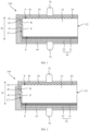
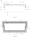
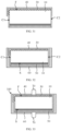
- FIG. 2 shows an embodiment that an edge of the first passivation layer 40 disposed on the first side surface C1 and away from the first surface F is located within the range of the flat region P.
- FIG. 1 shows an embodiment that an edge of the first passivation layer 40 away from the first surface F is flush with the surface of the passivating contact layer 50 away from the substrate 10. It can be understood that, as compared with the embodiment shown in FIG. 2 , the embodiment shown in FIG. 1 has better passivation effect.
- the edge of the first passivation layer 40 is flush with the edge of the doped conducting layer 30.
- the first passivation layer 40 does not extend to the flat region P along the thickness direction H of the substrate 10. That is, the coverage range of the first passivation layer 40 is consistent with the coverage range of the doped conducting layer 30.
- the second passivation layer 60 covers at least a portion of the first side surface C1, so as to cover at least a portion of the first passivation layer 40 on the first side surface C1. Since the first passivation layer 40 covers the first surface F and at least a portion of the first side surface C1 and the second passivation layer 60 covers at least a portion of the first passivation layer 40, the first passivation layer 40 and the second passivation layer 60 together protect at least a portion of the first side surface C1, which not only increases the passivation effect on at least a portion of the first side surface C1, but also alleviates the recombination of carriers at the first side surface C1.
- the second passivation layer 60 is an insulating layer, which can effectively prevent leakage currents at the first side surface C1, thereby increasing the output power of the solar cell 100 while improving the conversion efficiency of the solar cell 100.
- the second passivation layer 60 at least covers the second surface S and at least a portion of the first side surface C1, so as to cover the passivating contact layer 50 and at least a portion of the first passivation layer 40.
- the second passivation layer 60 can continuously cover the second surface S and at least a portion of the first side surface C1 adjacent to the second surface S, so that both the passivating contact layer 50 and the first passivation layer 40 can be covered.
- the second passivation layer 60 includes one portion covering the second surface S and another portion extending to the first side surface C1 continuously from the portion covering the second surface S.
- the coverage range of the second passivation layer 60 on the first side surface C1 is described below with reference to FIGs. 1 to 4 .
- the first passivation layer 40 extends to pass the edge of the doped conducting layer 30 along the thickness direction H of the substrate 10.
- the portion of the first passivation layer 40 located on the first side surface C1 can include a first portion 41 covering the flat region P, and the second passivation layer 60 can at least cover the first portion 41. In this way, it ensures that the second passivation layer 60 reliably covers the first passivation layer 40, preventing the region of the first side surface C1 between ends of the two passivation layers from being not covered by any passivation layer.
- the portion of the first passivation layer 40 located on the first side surface C1 further includes a second portion 42 covering the textured region R.
- the second passivation layer 60 covers the first portion 41 and at least a portion of the second portion 42. In this way, the coverage range of the second passivation layer 60 on the first passivation layer 40 is relatively large, improving the passivation effect on the side surface of the solar cell 100.
- the second passivation layer 60 covers the entire first portion 41 and a portion of the second portion 42. In other embodiments, the second passivation layer 60 only covers the first portion 41, or the second passivation layer 60 only covers the entire second portion 42.
- the second passivation layer 60 extends along the thickness direction H of the substrate 10, such that the edge of the second passivation layer 60 away from the second surface S is flush with the outer surface of the first passivation layer 40 on the first surface F. In this way, the passivation effect on the side surface of the solar cell 100 is improved.
- the first passivation layer 40 is not well or uniformly deposited due to contact with a quartz boat or due to manufacturing issues, the increased coverage range of the second passivation layer 60 can further improve the reliability of passivation on the side surface of the solar cell 100.
- the edge of the first passivation layer 40 is flush with the edge of the doped conducting layer 30, and the portion of the first passivation layer 40 disposed on the first side surface C1 only covers the textured region R.
- the second passivation layer 60 on the first side surface C1 covers at least a portion of the textured region R.
- the second passivation layer 60 on the first side surface C1 covers a portion of the textured region R.
- the second passivation layer 60 on the first side surface C1 extends along the thickness direction H of the substrate 10, such that the edge of the second passivation layer 60 away from the second surface S is flush with the outer surface of the first passivation layer 40 on the first surface F. In this way, the passivation effect on the side surface of the solar cell 100 is improved.
- the first passivation layer 40 is not well or uniformly deposited due to contact with a quartz boat or due to manufacturing issues, the increased coverage range of the second passivation layer 60 can further improve the reliability of passivation on the side surface of the solar cell 100.
- the second passivation layer 60 on the first side surface C1 can cover a portion of the textured region R, which may be due to following facts: During the manufacture process of the solar cell 100, a portion of the first passivation layer 40 on the first side surface C1 or on the cut edge side surface C2 of the substrate 10 may be in contact with a positioning member or the like and thus prevented from having a film or a layer formed thereon, so that the second passivation layer 60 does not completely cover the first passivation layer 40.
- the substrate 10 includes at least one cut edge side surface C2 adjacent to and between the first surface F and the second surface S.
- the textured structure 20 is only formed in the first surface F and a portion of the first side surface C1.
- the doped conducting layer 30 is only disposed on the first surface F and a portion of the first side surface C1, so as to cover the textured structure 20.
- the cut edge side surface C2 is flush with the edges of the doped conducting layer 30, the first passivation layer 40, the passivating contact layer 50, and the second passivation layer 60 on the same side as the cut edge side surface C2.
- no film or layer is formed on the surface of the solar cell 100 corresponding to the cut edge side surface C2.
- Such a structure may be obtained by cutting a cell structure at the end of the manufacture process of the solar cell 100.
- the solar cells 100 based on the above embodiments are further improved by forming a film or layer structure on the cut edge side surface C2. It can be understood that the film or layer structures and the coverage ranges thereof on the first surface F and the first side surface C1 of the substrate 10 are the same as those in the above embodiments, which will not be repeatedly described herein.
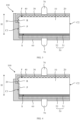
- FIG. 5 and FIG. 6 show embodiments that the first passivation layer 40 on the first side surface C1 extends beyond the edge of the doped conducting layer 30 along the thickness direction H of the substrate 10.
- FIG. 7 and FIG. 8 show embodiments that the edge of the first passivation layer 40 on the first side surface C1 is flush with the edge of the doped conducting layer 30.
- FIG. 5 and FIG. 7 show embodiments that the second passivation layer 60 on the first side surface C1 extends along the thickness direction H of the substrate 10, such that the edge of the second passivation layer 60 is flush with the outer surface of the first passivation layer 40 on the first surface F.
- FIG. 6 and FIG. 8 show the embodiments that the second passivation layer 60 partially covers the second portion 42, which is the portion of the first passivation layer 40 located on the first side surface C 1 and covering the textured structure R.
- the arrangement of the films or layers on the cut edge side surface C2 is as follows.
- the textured structure 20 is only formed in the first surface F and a portion of the first side surface C1.
- the doped conducting layer 30 is only formed on the first surface F and a portion of the first side surface C1 to cover the textured structure 20.
- the textured structure 20 and the doped conducting layer 30 are not formed on the cut edge side surface C2.
- the first passivation layer 40 also covers at least a portion of the cut edge side surface C2.
- the cut edge side surface C2 corresponds to the cut-formed surface of the solar cell 100, so that at least a portion of the cut edge side surface C2 is protected by the first passivation layer 40, which not only increases the passivation effect on the cut edge side surface C2, but also alleviates the recombination of carriers at the cut edge side surface C2.
- the first passivation layer 40 is an insulating layer, which effectively prevents leakage currents at the cut edge side surface C2, thereby increasing the output power while improving the conversion efficiency of the solar cell 100.
- the coverage range of the first passivation layer 40 on the cut edge side surface C2 can be as follows.
- the edge of the first passivation layer 40 can be located on the cut edge side surface C2 and away from the first surface F, being flush with the surface of the passivating contact layer 50 away from the substrate 10.
- the edge of the first passivation layer 40 located on the cut edge side surface C2 and away from the first surface F can be located within the range of the cut edge side surface C2.
- the edge of the first passivation layer 40 on the first side surface C1 can be flush with the other edge of the first passivation layer 40 on the cut edge side surface C2.
- the edge of the first passivation layer 40 on the first side surface C1 is not flush with the other edge of the first passivation layer 40 on the cut edge side surface C2.
- the second passivation layer 60 also covers at least a portion of the cut edge side surface C2, so as to cover at least a portion of the first passivation layer 40 on the cut edge side surface C2.
- the second passivation layer 60 on the cut edge side surface C2 extends along the thickness direction H of the substrate 10, such that the edge of the second passivation layer 60 is flush with the outer surface of the first passivation layer 40 on the first surface F.
- the second passivation layer 60 only covers a portion of the first passivation layer 40 on the cut edge side surface C2.
- the edge of the second passivation layer 60 on the first side surface C1 can be flush with the other edge of the second passivation layer 60 on the cut edge side surface C2.
- the edge of the second passivation layer 60 on the first side surface C1 is not flush with the other edge of the second passivation layer 60 on the cut edge side surface C2.
- the solar cells 100 based on the above embodiments are further improved by forming a film or layer structure on the cut edge side surface C2. It can be understood that the film or layer structures and the coverage ranges thereof on the first surface F and the first side surface C1 of the substrate 10 are the same as those in the above embodiments, which will not be repeatedly described herein.
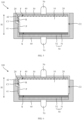
- FIG. 9 and FIG. 10 show embodiments that the first passivation layer 40 on the first side surface C1 extends beyond the edge of the doped conducting layer 30 along the thickness direction H of the substrate.
- FIG. 11 and FIG. 12 show embodiments that the edge of the first passivation layer 40 on the first side surface C1 is flush with the edge of the doped conducting layer 30.
- FIG. 9 and FIG. 11 show embodiments that the second passivation layer 60 on the first side surface C1 extends along the thickness direction H of the substrate 10, such that the edge of the second passivation layer 60 is flush with the outer surface of the first passivation layer 40 on the first surface F.
- FIG. 10 and FIG. 12 show embodiments that the second passivation layer 60 partially covers the second portion 42.
- the arrangement of the films or layers on the cut edge side surface C2 is as follows.
- the textured structure 20 is also formed in at least a portion of the cut edge side surface C2.
- the doped conducting layer 30 is disposed on the first surface F, a portion of the first side surface C1, and a portion of the cut edge side surface C2, so as to cover the textured structure 20.
- the first passivation layer 40 also covers at least a portion of the cut edge side surface C2, so as to cover at least the doped conducting layer 30.
- the doped conducting layer 30 completely covers the textured structure 20 on the cut edge side surface C2.
- the first passivation layer 40 completely covers the doped conducting layer 30 on the cut edge side surface C2.
- the cut edge side surface C2 also includes the textured structure 20 and the doped conducting layer 30 is disposed on the textured structure 20, the doped conducting layer 30 on this region is conducive to reducing the recombination of carriers at interface at the cut edge side surface C2, thereby achieving a relatively good passivation effect on the cut edge side surface C2.
- the textured structure 20 in the cut edge side surface C2 increases the light absorption area of the solar cell 100, thereby increasing the photogenerated current of the solar cell 100, which is conducive to the efficiency of the solar cell 100.
- the first passivation layer 40 at least covers at least a portion of the cut edge side surface C2, so as to cover at least the doped conducting layer 30, so that at least a portion of the cut edge side surface C2 is protected by the first passivation layer 40, which not only increases the passivation effect on the cut edge side surface C2, but also alleviates the recombination of carriers at the cut edge side surface C2.
- the first passivation layer 40 is an insulating layer, which can effectively prevents leakage currents at the cut edge side surface C2, thereby increasing the output power while improving the conversion efficiency of the solar cell 100.
- the coverage range of the first passivation layer 40 on the cut edge side surface C2 can be as follows.
- the first passivation layer 40 on the cut edge side surface C2 extends along the thickness direction H of the substrate 10, such that the edge of the first passivation layer 40 away from the first surface F is flush with the surface of the passivating contact layer 50 away from the substrate 10.
- the edge of the first passivation layer 40 away from the first surface F is flush with the edge of the doped conducting layer 30.
- the first passivation layer 40 extends beyond the edge of the doped conducting layer 30, and the edge of the first passivation layer 40 away from the first surface F is located within the range of the cut edge side surface C2.
- the edge of the first passivation layer 40 on the first side surface C1 can be flush with the other edge of the first passivation layer 40 on the cut edge side surface C2.
- the edge of the first passivation layer 40 on the first side surface C1 is not flush with the other edge of the first passivation layer 40 on the cut edge side surface C2.
- the second passivation layer 60 also covers at least a portion of the cut edge side surface C2, so as to cover at least a portion of the first passivation layer 40 on the cut edge side surface C2.
- the second passivation layer 60 on the cut edge side surface C2 extends along the thickness direction H of the substrate, such that the edge of the second passivation layer 60 is flush with the outer surface of the first passivation layer 40 on the first surface F.
- the second passivation layer 60 only covers a portion of the first passivation layer 40 on the cut edge side surface C2.
- the edge of the second passivation layer 60 on the first side surface C1 can be flush with the other edge of the second passivation layer 60 on the cut edge side surface C2.
- the edge of the second passivation layer 60 on the first side surface C1 is not flush with the other edge of second passivation layer 60 on the cut edge side surface C2.
- first side surface C1 and one cut edge side surface C2 are taken as example for above description.
- the substrate 10 includes a plurality of first side surfaces C1 and/or a plurality of cut edge side surfaces C2
- the plurality of first side surfaces C1 and/or the plurality of cut edge side surfaces C2 as well as the films or layers thereon can respectively have same or different structures.
- the above embodiments can be arbitrarily combined and applied to the plurality of first side surfaces C1 and/or the plurality of cut edge side surfaces C2.
- the doped conducting layer 30 can be formed by diffusing doping elements to at least a portion of a surface of the substrate 10.
- Both the first passivation layer 40 and the second passivation layer 60 can be formed by using a deposition method, such as plasma-enhanced chemical vapor deposition. Therefore, the outer surfaces of the doped conducting layer 30, the first passivation layer 40, and the second passivation layer 60 may be non-flat but have conformal structures corresponding to the surfaces of the substrate 10.
- the doped conducting layer 30, the first passivation layer 40, and/or the second passivation layer 60 also have a textured structure.
- the doped conducting layer 30, the first passivation layer 40, and/or the second passivation layer 60 also have flat surfaces.
- An embodiment of the present application provides a method for manufacturing a solar cell.
- the method is adapted to manufacture the solar cell in any of the above embodiments.
- the structures, functions, working principles, etc. relating to the solar cell 100 that have been described in the above embodiments may not be repeated herein.
- the method for manufacturing the solar cell includes steps S10 to S40.
- the wafer 101 includes a substrate 10 and a doped conducting layer 30.
- the substrate 10 includes a first surface F, a second surface S, and at least one first side surface C1.
- the first surface F and second surface S are opposite to each other.
- the at least one first side surface C1 is adjacent to and between the first surface F and the second surface S.
- At least the first surface F and a portion of the first side surface C1 of the substrate 10 include a textured structure 20.
- the doped conducting layer 30 is disposed at least on the first surface F and a portion of the first side surface C1 to cover the textured structure 20.
- the first passivation layer 40 covers the first surface F and at least a portion of the first side surface C1, so as to cover at least the doped conducting layer 30.
- the second passivation layer 60 covers the second surface S, so as to cover the passivating contact layer 50.
- the first surface F and a portion of the first side surface C1 of the substrate 10 include a textured structure 20.
- the doped conducting layer 30 is at least disposed on the first surface F and at least a portion of the first side surface C1, so as to cover the textured structure 20. Since a portion of the first side surface C1 has the textured structure and the doped conducting layer 30 is disposed on the textured structure 20, the doped conducting layer 30 on the first side surface C1 is conducive to reducing recombination of carriers at interface at the first side surface C1, thereby achieving relatively good passivation effect on the first side surface C1.
- the textured structure 20 in the first side surface C1 increases the light absorption area of the solar cell 100, increasing the photogenerated current of the solar cell 100, which is conducive to increasing the efficiency of the solar cell 100.
- the first passivation layer 40 is formed on the doped conducting layer 30.
- the first passivation layer 40 covers at least the first surface F and at least a portion of the first side surface C1, so as to cover at least the doped conducting layer 30.
- at least a portion of the first side surface C1 is protected by the first passivation layer 40, which not only increases the passivation effect on the first side surface C1, but also alleviates the recombination of carriers at the first side surface C1.
- the first passivation layer 40 is an insulating layer, which effectively prevents leakage currents at the first side surface C1, thereby increasing the output power and the conversion efficiency of the solar cell 100.
- the structures, materials, and coverage ranges of the texture structure 20, the doped conducting layer 30, the first passivation layer 40, the passivating contact layer 50, and the second passivation layer 60 have been described in detail in the above embodiments and will not be repeatedly described herein.
- step S20 the step of forming the passivating contact layer 50 on the second surface S of the substrate 10 includes steps of:
- the tunnel material layer remained on the second surface S is the tunnel oxide layer 51.
- the doped polysilicon material layer remained on the second surface S is the doped polysilicon conducting layer 52.
- the oxide material layer for example, a silicon oxide layer, can function as a mask in a subsequent manufacture process, and can be removed by a subsequent process such as etching. In this way, the passivating contact layer 50 can be formed on the second surface S.
- the oxide material layers is etched and thus removed by using a continuous-type machine; the tunnel material layer and the doped polysilicon material layer are etched and thus removed by using a through-type machine.
- the method further includes a step of respectively forming electrodes 70 on the first passivation layer 40 and the second passivation layer 60.
- the electrode 70 at the first surface F side of the substrate 10 penetrates the first passivation layer 40 and is electrically connected to the doped conducting layer 30.
- the electrode 70 at the second surface S side of the substrate 10 penetrates the second passivation layer 60 and is electrically connected to the passivating contact layer 50.
- the cell with a standard size can be cut into halves or cut into multiple parts, which can be then connected in series to form a module.
- the cutting step can be performed at different stages.
- the cutting step can be performed in step S10.
- the cutting step can be performed after step S40.
- the cutting step can be performed between steps S10 and S40.
- the cutting step is specifically referred to cutting a substrate blank into substrates 10 with sizes as required by solar cells 100.
- the substrate blank before doping and texturing, can be cut into substrates 10 with suitable sizes corresponding to the sizes of the actual required solar cells 100.
- the edge surfaces of the solar cell 100 including the cut edge side surface C2 can be effectively passivated, thereby reducing recombination of carriers, and improving photoelectric conversion efficiency.
- no cutting step is performed in the subsequent steps, avoiding forming new cut surfaces, which effectively avoids significant carrier recombination occurring at the cut-formed surface in the related art.
- step S10 the step of providing the wafer 101 includes:
- all surfaces of the substrate 10 can be textured and formed into textured surfaces.
- the first surface F of the substrate 10 can be doped with the dopant elements to form the doped conducting layer 30, and some of the dopant elements wrap around the substrate 10 and deposit on the first side surface C1, the cut edge side surface C2, and the second surface S of the substrate 10, so that the first side surface C1, the cut edge side surface C2 and the second surface S are also covered with the doped conducting material.
- the first side surface C1, the cut edge side surface C2, and the second surface S of the substrate 10 can be etched by using a single-side etching technique, so as to remove the doped conducting material and the textured structure from the second surface S, the first target region C11 of the first side surface C1, and the second target region C12 of the cut edge side surface C2 of the substrate 10, thereby exposing the second surface S, the first target region C11 of the first side surface C1, and the second target region C12 of the cut edge side surface C2 of the substrate 10 to avoid leakage.
- the textured structure 20 and the doped conducting layer 30 located on the first surface F, a portion of the first side surface C1, and a portion of the cut edge side surface C2 are remained and thus formed.
- the step of etching the substrate 10 to expose the second surface S, the first target region C11 of each first side surface C1, and the second target region C12 of each cut edge side surface C2 of the substrate 10 includes step D and step E.
- Step D Etch the substrate 10 subjected to the texturing treatment and diffusion of dopant elements, so as to expose the textured structure in the second surface S, the first target region C11 of each first side surface C1, and the second target region C12 of each cut edge side surface C2.
- the etching can be performed by using a continuous-type machine. During the etching process, the liquid level in the continuous-type machine needs to be controlled to avoid the etching solution being in contact with the textured structure 20 and the doped conducting layer 30 on the first surface F of the substrate 10.
- the morphology on the first side surface C1 is irregular as shown in FIG. 20 .
- Step E Etch to remove the exposed textured structure in the second surface S, the first target region C11, and the second target region C12, so as to expose the second surface S, the first target region C11 of each first side surface C1, and the second target region C12 of each cut edge side surface C2 of the substrate 10.
- the etching can be performed by using a through-type machine. It can be understood that etching to remove the exposed textured structure is to polish the exposed textured structure, so as to form a non-textured structure, such as a relatively flat surface. Due to the slight fluctuations of the surface of the etching solution and the soaking of the substrate 10 with the etching solution during the etching process, as shown in FIG. 20 , the boundary line 11 between the doped conducting layer 30 and the first target region C11 may be not a straight line, but exhibits an irregular wavy pattern.
- the step of cutting the substrate blank along the thickness direction to form the substrates 10 includes a step of laser cutting the substrate blank along the thickness direction H to form the substrates 10.
- the substrate blank can be divided into two substrates 10 by one laser cutting step.
- Example 1 A method for manufacturing a solar cell includes steps SJ to SO.
- Step SJ Referring to FIG. 14 , a substrate blank is cut along the thickness direction H to form at least two substrates 10.
- Each substrate 10 includes a first surface F and a second surface S opposite to each other, and includes a plurality of first side surfaces C1 adjacent to and between the first surface F and the second surface S, and further includes at least one cut edge side surface C2 formed by a cutting step.
- Step SK Referring to FIG. 15 , surfaces of the substrate 10 are textured and diffused with boron elements.
- the substrate 10 is then etched to expose the second surface S, the first target region C11 of each first side surface C1, and the second target region C12 of each cut edge side surface C2 of the substrate 10, so as to remain the textured structure 20 in the first surface F, a portion of each first side surface C1, and a portion of each cut edge side surface C2 of the substrate 10, and remain a doped conducting layer 30 (i.e., the boron-doped conducting layer) covering the textured structure 20 of the first surface F, a portion of each first side surface C1, and a portion of each cut edge side surface C2 of the substrate 10, thereby forming a wafer 101.
- a doped conducting layer 30 i.e., the boron-doped conducting layer
- Step SL A tunnel material layer, a doped polysilicon material layer, and an oxide material layer are sequentially stacked on surfaces of the wafer 101.
- the oxide material layer on the surface F' of the first side of the wafer 101 and on the side surfaces of the wafer 101 (including every first side surface C1 and every cut edge side surface C2) are etched thereby being removed.
- the doped polysilicon material layer and the tunnel material layer on the surface F' of the first side of the wafer 101 and on the side surfaces of the wafer 101 are etched thereby being removed.
- the surface F' of the first side of the wafer 10 corresponds to the first surface F of the substrate 10. In this way, only the tunnel material layer, the doped polysilicon material layer, and the oxide material layer on the second surface S remain.
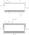
- the tunnel material layer for example, a silicon oxide layer, can function as a mask in a subsequent manufacture process, and can be removed by a subsequent process such as etching. In this way, a passivating contact layer 50 can be formed on the second surface S, as shown in FIG. 16 .
- Step SM Referring to FIG. 17 , a first passivation layer 40 is formed on the doped conducting layer 30.
- the first passivation layer 40 at least covers the first surface F, at least a portion of each first side surface C1, and at least a portion of each cut edge side surface C2, so as to at least cover the doped conducting layer 30.
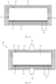
- Step SN Referring to FIG. 18 , a second passivation layer 60 is formed on the passivating contact layer 50.
- the second passivation layer 60 at least covers the second surface S, at least a portion of each first side surface C1, and at least a portion of each cut edge side surface C2, so as to cover the passivating contact layer 50 and at least a portion of the first passivation layer 40.
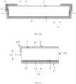
- Step SO Referring to FIG. 19 , electrodes 70 are respectively formed on the first passivation layer 40 and the second passivation layer 60, thereby achieving a solar cell 100.
- the solar cell 100 manufactured through steps SJ to SO will be referred to as solar cell A1.
- Comparative Example 1 A method for manufacturing a solar cell includes steps SP to SU.
- Step SP A silicon substrate is washed and textured, and then the washed and textured front surface of the silicon substrate is diffused with boron elements.
- Step SQ The borosilicate glass (BSG), formed on the back surface and the side surfaces of the silicon substrate due to wraparound deposition of boron, is removed, and the side surfaces and the back surface of the silicon substrate are polished with alkali.
- BSG borosilicate glass
- Step SR A tunnel oxide layer and a doped polysilicon conducting layer are stacked on the back surface of the silicon substrate.
- Step SS A passivation and anti-reflection film is deposited on both the front surface and the back surface of the silicon substrate.
- Step ST Electrodes are respectively formed on both the front surface and the back surface of the silicon substrate to achieve a solar cell.
- Step S U The solar cell is cut in half by a laser.
- the solar cell manufactured through the steps SP to ST of the comparative example will be referred to as solar cell B1.
- the solar cell manufactured through the steps SP to SU of the comparative example will be referred to as solar cell B2.
- the solar cell A1 and the solar cells B1 and B2 were subjected to performance tests.
- the test results were recorded in Table 1, wherein Uoc represents the open circuit voltage, FF represents the fill factor, Eta represents the conversion efficiency, Isc represents the short-circuit current, and IRev2 represents the reverse current.
- Table 1 Test results of performance of solar cells Solar cell Isc (A) Uoc (mV) FF (%) Eta (%) IRev2 (A) A1 7.79 712.9 82.95 24.13 0.05 B1 15.56 713.3 82.98 24.12 0.08 B2 7.76 712.2 82.21 23.80 0.09
- the efficiency of the solar cell A1 (being cut) prepared by the method in Example 1 is substantially the same as the efficiency of the intact solar cell B1 (uncut) in Comparative Example 1.
- the open circuit voltage of the solar cell A1 increased by 0.7 mV
- the fill factor of the solar cell A1 increased by about 0.74%
- the conversion efficiency of the solar cell A1 increased by about 0.33%
- the reverse current of the solar cell A1 decreased from 0.09A to 0.05. It can be seen that the solar cell A1 prepared by the method in Example 1 has a higher efficiency.
- the cutting step is performed in step S10. In some other embodiments, the cutting step can be performed after step S40. For example, the cutting step is performed after the preparation of the films and layers.
- step S50 the cutting step is performed after step S40, after step S40 of forming the second passivation layer 60 on the passivating contact layer 50, the method further includes step S50:
- Step S50 laser cut the solar cell matrix 103 (e.g., as shown in FIG. 25 ) along the thickness direction to form the cut edge side surface C2 of the substrate 10.
- the solar cell matrix 103 can be divided into two or more solar cells 100 by the cutting step.
- the solar cell matrix 103 can be cut into halves along the thickness direction H to form two solar cells 100 (e.g., as shown in FIG. 26 ).
- the step of forming the electrodes 70 on the first passivation layer 40 and the second passivation layer 60 can be performed before step S50.
- step S10 the substrate 10 is not formed from cutting the substrate blank and thus only includes the first side surfaces C1, not including any cut edge side surface C2.
- step S10 the step of providing the wafer 101 includes:
- all surfaces of the substrate 100 can be textured and formed into textured surfaces.
- the first surface F of the substrate 10 can be doped with the dopant elements to form the doped conducting layer 30, and some of the dopant elements wrap around the substrate 10 and deposit to the first side surface C1 and the second surface S of the substrate 10, so that the first side surface C1 and the second surface S are also covered with the doped conducting material.
- the first side surface C1 and the second surface S of the substrate 10 can be etched by using a single-side etching technique, so as to remove the doped conducting material and the textured structure from the second surface S and the first target region C11 of the first side surface C1 of the substrate 10, thereby exposing the second surface S and the first target region C11 of the first side surface C1 of the substrate 10 to avoid leakage.
- the textured structure 20 and the doped conducting layer 30 located on the first surface F and a portion of the first side surface C1 are remained and thus formed.
- the step of etching the substrate 10 to expose the second surface S and the first target region C11 of each first side surface C1 of the substrate 10 includes step D' and step E'.
- Step D' Etch the substrate 10 subjected to the texturing treatment and diffusion of dopant elements, so as to expose the textured structures in the second surface S and each first target region C11.
- the etching can be performed using a continuous-type machine. During the etching process, the liquid level in the continuous-type machine needs to be controlled to avoid the etching solution being in contact with the textured structure 20 and the doped conducting layer 30 on the first surface F of the substrate 10.
- the morphology on the first side surface C1 is irregular as shown in FIG. 20 .
- Step E' Etch to remove the exposed textured structure, so as to expose the second surface S and the first target region C11 of each first side surface C1 of the substrate 10.
- the etching can be performed by using a through-type machine. It can be understood that etching to remove the exposed textured structure of the surface of the substrate 10 is to polish the textured structure 20 of the first target region C11 and the second surface S of the substrate 10, so as to form a non-textured structure, such as a relatively flat surface. Due to the slight fluctuations of the surface of the etching solution and the soaking of the substrate 10 with the etching solution during the etching process, as shown in FIG. 20 , the boundary line 11 between the doped conducting layer 30 and the first target region C 11 may not be a straight line, but exhibits an irregular wavy pattern.
- the size of the finally formed solar cell 100 (e.g., as shown in FIG. 26 ) is smaller than the size of the solar cell matrix 103 (e.g., as shown in FIG. 25 ).
- a cut surface CQ formed by the cutting is formed, e.g., as shown in FIG. 27 .
- Example 2 A method of manufacturing a solar cell including steps SJ' to SO'.
- Step SJ' Referring to FIG. 21 , surfaces of a substrate 10 are textured and diffused with boron elements.
- the substrate 10 is then etched to expose the second surface S and the first target region C11 of each first side surface C1, so as to remain the textured structure 20 in the first surface F and a portion of each first side surface C1 of the substrate 10, and remain a doped conducting layer 30 (i.e., the boron-doped conducting layer) covering the textured structure 20 of the first surface F and a portion of the first side surface C1, thereby forming a wafer 101.
- a doped conducting layer 30 i.e., the boron-doped conducting layer
- Step SK' Referring to FIG. 22 , a tunnel material layer, a doped polysilicon material layer, and a silicon oxide material layer are sequentially stacked on surfaces of the wafer 101.
- the silicon oxide material layer on the surface F' of the first side of the wafer 101 and on the side surfaces of the wafer 101 are etched thereby being removed.
- the tunnel material layer and the doped polysilicon material layer on the surface F' of the first side of the wafer 101 and on the side surfaces of the wafer 101 are etched thereby being removed.
- the tunnel material layer, the doped polysilicon material layer, and the oxide material layer on the second surface S remain.
- the silicon oxide material layer for example, a silicon oxide layer, can function as a mask in a subsequent manufacture process, and can be removed by a subsequent process such as etching. In this way, a passivating contact layer 50 can be formed on the second surface S, as shown in FIG. 22 .
- Step SL' Referring to FIG. 23 , a first passivation layer 40 is formed on the doped conducting layer 30.
- the first passivation layer 40 at least covers the first surface F and entire of each first side surface C1, so as to cover the doped conducting layer 30.
- Step SM' Referring to FIG. 24 , a second passivation layer 60 is formed on the passivating contact layer 50 to form a solar cell matrix 103.
- the second passivation layer 60 covers the second surface S and the entire of each first side surface C1, so as to cover the passivating contact layer 50 and completely cover the first passivation layer 40 disposed on the first side surface C1.
- Step SN' Referring to FIG. 25 , electrodes 70 are respectively formed on the first passivation layer 40 and the second passivation layer 60 of the solar cell matrix 103.
- Step SO' Referring to FIG. 26 , the solar cell matrix 103 is cut by a laser along the thickness direction H, so as to form at least two solar cells 100.
- the solar cell 100 manufactured through steps SJ' to SO' will be referred to as solar cell A2.
- the solar cell A2 and the solar cell B1 were subjected to performance tests.
- the test results were recorded in Table 2, wherein Uoc represents the open circuit voltage, FF represents the fill factor, Eta represents the conversion efficiency, Isc represents the short-circuit current, and IRev2 represents the reverse current.
- Table 2 Test results of performance of solar cells Solar cell Isc (A) Uoc (mV) FF (%) Eta (%) IRev2 (A) A2 15.57 714.4 83.00 24.18 0.05 B1 15.56 713.3 82.98 24.12 0.08
- the laser cutting technology results in high carrier recombination at the cut edges of the resulting half-cells, creating a large number of dangling bonds and defect states at the surfaces, which become effective recombination centers for carriers.
- the cut edges of the half-cells are prone to have a leakage problem, ultimately reducing the efficiency of the solar cell.
- the cutting step is performed in the manufacture process of the solar cell, after the deposition of the passivating contact material.
- the cut-formed surface is further passivated by the first passivation layer and the second passivation layer that are subsequently deposited, which alleviates the carrier recombination at the cut-formed surface and increases the efficiency of the solar cell 100.
- An embodiment of the present application provides another method for manufacturing a solar cell, which is adapted to manufacture the solar cell 100 in any of the above embodiments.
- the structures, functions, working principles, etc. relating to the solar cell 100 that have been described in the above embodiments may not be repeated herein.
- the cutting step is performed during the step of forming the passivating contact layer 50.
- the method for manufacturing the solar cell provided in the present embodiment includes S100 to S500.
- the wafer 101' includes a substrate 10 and a doped conducting material layer 30'.
- the substrate 10 includes a first surface F, a second surface S, and at least one first side surface C1.
- the first surface F and the second surface S are opposite to each other.
- the at least one first side surface C1 is adjacent to and between the first surface F and the second surface S.
- At least the first surface F and a portion of the first side surface C1 of the substrate 10 include a textured structure 20.
- the doped conducting material layer 30' is disposed at least on the first surface F and a portion of the first side surface C1 to cover the textured structure 20.
- the cutting step divides the wafer 101' into at least two sub-wafers 102.
- the surface F' of the first side of the sub-wafer 20 corresponds to the first surface F of the substrate 10.
- the first passivation layer 40 covers at least the first surface F and at least a portion of the first side surface C1, so as to at least cover the doped conducting layer 30.
- the first passivation layer 40 further covers at least a portion of the cut edge side surface C2.
- the cut edge side surface C2 is a side surface of the sub-wafer formed by cutting the wafer 101'.
- the first surface F and a portion of the first side surface C1 of the substrate 10 include a textured structure 20.
- the doped conducting material layer 30' is at least disposed on the first surface F and at least a portion of the first side surface C1, so as to cover the textured structure 20. Since a portion of the first side surface C1 has the textured structure and the doped conducting material layer 30' is disposed on the textured structure 20, the doped conducting material layer 30' on the first side surface C1 in the cut solar cell 100 is conducive to reducing recombination of carriers at the interface at the first side surface C1, thereby achieving relatively good passivation effect on the first side surface C1.
- the textured structure 20 in the first side surface C1 increases the light absorption area of the solar cell 100, increasing the photogenerated current of the solar cell 100, which is conducive to the efficiency of the solar cell 100.
- the first passivation layer 40 is formed on the doped conducting layer 30.
- the first passivation layer 40 covers at least a portion of the cut edge side surface C2, so that at least a portion of the cut edge side surface C2 is protected by the first passivation layer 40, which not only increases the passivation effect on the cut edge side surface C2, but also alleviates the recombination of carriers generated at the cut edge side surface C2.
- the first passivation layer 40 is an insulating layer, which c effectively prevents leakage currents at the cut edge side surface C2, thereby increasing the output power and the conversion efficiency of the solar cell 100.
- the first passivation layer 40 at least covers the first surface F and at least a portion of the first side surface C1, so as to cover at least the doped conducting layer 30. Since the first passivation layer 40 covers the first surface F and at least a portion of the first side surface C1, at least a portion of the first side surface C1 is protected by the first passivation layer 40, which not only increases the passivation effect on the first side surface C1, but also alleviates the recombination of carriers at the first side surface C1. In addition, the first passivation layer 40 is an insulating layer, which effectively prevents leakage currents at the first side surface C1, thereby increasing the output power and the conversion efficiency of the solar cell 100.
- the wafer 101' is cut into at least two sub-wafers 102. That is, the solar cell 100 is achieved after the wafer 101' is cut in step S300.
- the size of the substrate 10 in the wafer 101' is larger than the size of the substrate 10 in the solar cell 100.
- the first surface F and the second surface S of the substrate 10 in the wafer 101' is the same as those in the finally formed solar cell 100, which will not be repeatedly described herein.
- the wafer 101' is cut into a plurality of sub-wafers 102, so that the size of some first side surfaces C1 of the substrate 10 of each sub-wafer 102 is reduced as compared with the original substrate 10, while a new surface formed by cutting (i.e., the cut edge side surface C2) is formed in the substrate 10 of the sub-wafer 102 (and of the solar cell 100).
- a plurality of first side surfaces C1 of the substrate 10 can be connected to each other and jointly surrounds the first surface F.
- Each first side surface C1 is connected to the first surface F and the second side S.
- the first surface F and a portion of the first side surface C1 of the substrate 10 include the textured structure 20, which is similar to that in the above embodiments.
- the textured structure 20 of the first surface F and the textured structure 20 of the first side surface C1 can form a continuous structure or a discontinuous structure. In this way, when a continuous structure is formed, the textured structure 20 as a whole forms a cover enveloping the first surface F of the substrate 10.
- the doped conducting layer 30 is formed from the doped conducting material layer 30' after the cutting step in step S300.
- the material, structure, and coverage range of the doped conducting material layer 30' are the same as those of the doped conducting layer 30 in the above embodiments, which will not be repeatedly described herein.
- the doped conducting material layer 30' is formed on the first surface F and a portion of each first side surface C1 to cover the textured structure 20. Therefore, a portion of the doped conducting material layer 30' is disposed on the first surface F, and another portion of the doped conducting material layer 30' is disposed on a portion of each first side surface C1.
- the coverage range of the doped conducting material layer 30' covers the textured structure 20. In some embodiments, the coverage range of the doped conducting material layer 30' may be larger than the coverage range of the textured structure 20. In some embodiments, the coverage range of the doped conducting material layer 30' is identical to the coverage range of the textured structure 20. That is, the doped conducting material layer 30' only and completely covers the textured structure 20.
- step S200 during forming the passivating contact material layer 50' on the second surface S of the substrate 10 of the wafer 101', the passivating contact material layer 50' will also be formed on the surface of the first side and each side surface of the wafer 101'.
- step S400 except the passivating contact material layer 50' on the second surface S of the substrate 10 of the sub-wafer 102 formed by the cutting step, the passivating contact material layer 50' on all other surface is etched and thus removed, thereby forming the passivating contact layer 50.
- the material of the passivating contact material layer 50' is the same as that of the passivating contact layer 50 in the above embodiments.
- the passivating contact material layer 50' can include a tunnel material layer 51' and a doped polysilicon material layer 52' stacked on the second surface S in sequence.
- the tunnel material layers 51' and 51 are the same in material and structure, and the doped polysilicon material layers 52' and 52 are the same in material and structure, which will not be repeatedly described herein.
- step S500 the first passivation layer 40 is formed on the doped conducting layer 30.
- the first passivation layer 40 has been described in detail in the above embodiments and will not be described repeatedly herein.
- step S100 referring to FIG. 29A , the step of providing the wafer 101' includes:
- the first target region C11 is a region of each first side surface C1 of the substrate 10 adjacent to and connected to the second surface S.
- all surfaces of the substrate 10 can be textured and formed into textured surfaces.
- the first surface F of the substrate 10 can be doped with the dopant elements to form the doped conducting material layer 30', and some of the dopant elements wrap around the substrate 10 and deposit on the first side surface C1 and the second surface S of the substrate 10, so that the first side surface C1 and the second surface S are also covered with the doped conducting material.
- the first side surface C1 and the second surface S of the substrate 10 are etched by using a single-side etching technique, so as to remove the doped conducting material and the textured structure from the second surface S and the first target region C11 of the first side surface C1 of the substrate 10, thereby exposing the second surface S and the first target region C11 of each first side surface C1 of the substrate 10 to avoid leakage.
- the textured structure 20 and the doped conducting material layer 30' located on the first surface F and a portion of the first side surface C1 are remained and thus formed.
- the step of etching the substrate 10 to expose the second surface S and the first target region C11 of each first side surface C1 of the substrate 10 includes step D" and step E".
- Step D Etch the substrate 10 subjected to the texturing treatment and diffusion of dopant elements, so as to expose the textured structure in the second surface S and the first target region C11 of each first side surface C1.
- the etching can be performed by using a continuous-type machine. During the etching process, the liquid level in the continuous-type machine needs to be controlled to avoid the etching solution being in contact with the textured structure 20 and the doped conducting material layer 30' on the first surface F of the substrate 10, so that after the etching step, the morphology on the first side surface C1 is irregular.
- Step E" Etch to remove the exposed textured structure, so as to expose the second surface S and the first target region C11 of each first side surface C1 of the substrate 10.
- the etching can be performed by using a through-type machine. It can be understood that etching to remove the textured structure 20 in the surface of the substrate 10 is to polish the textured structure 20 of the first target region C11 and the second surface S of the substrate 10, so as to form a non-textured structure, such as a relatively flat surface.
- the step of forming the passivating contact material layer 50' on each surface of the wafer 101' includes a step of sequentially forming a tunnel material layer 51', a doped polysilicon material layer 52', and an oxide material layer (i.e., a mask layer) on each surface of the wafer 101'.
- step S400 the step of etching to remove the passivating contact material layer 50' on the surface of the first side and each side surface of the sub-wafer 102, so as to form the passivating contact layer 50 on the sub-wafer 102 includes: etching to remove the oxide material layer on the surface F' of the first side of the sub-wafer 102 and on each side surface of the sub-wafer 102;
- the cut edge side surface C2 formed by the cutting step can be etched and polished to remove the laser-damaged surface layer, thereby reducing the recombination of carriers at the interface of the cut edge side surface C2.
- the step of etching to remove the oxide material layer is performed by using a through-type machine.
- the step of etching to remove the doped polysilicon material layer 52' and the tunnel material layer 51' is performed by using a trough-type machine.
- the method further includes: etching to remove the oxide material layer on a surface S' of a second side of the sub-wafer 102, thereby forming the passivating contact layer 50 on the sub-wafer 102, wherein the surface S' of the second side of the sub-wafer 102 corresponds to the second surface S of the substrate 10.
- step S300 the step of cutting the wafer 101 formed with the passivating contact material layer 50' along the thickness direction H of the substrate to form at least two sub-wafers 102 includes: laser cutting the wafer 101 formed with the passivating contact material layer 50' along the thickness direction H of the substrate 10 to form the sub-wafers 102.
- one wafer 101 can be divided into two equal sized sub-wafers 102 by one laser cutting step. It can be understood that, in the sub-wafer 102, the substrate 10, the textured structure 20, and the doped conducting layer 30 can be the same as that in the solar cell 100 in the above embodiments.
- step S500 after the step of forming the first passivation layer 40 on the doped conducting layer 30, the method further includes: forming a second passivation layer 60 on the passivating contact layer 50, wherein the second passivation layer 60 covers at least the second surface S, at least a portion of each first side surface C1, and at least a portion of each cut edge side surface C2, so as to cover the passivating contact layer 50 and at least a portion of the first passivation layer 40.
- the first passivation layer 40 and the second passivation layer 60 together protect at least a portion of the first side surface C1 and at least a portion of the cut edge side surface C2, which not only increases the passivation effect on the first side surface C1 and the cut edge side surface C2, but also alleviates the recombination of carriers at the side surface of the solar cell 100.
- the first passivation layer 40 and the second passivation layer 60 are insulating layers, which can effectively prevent leakage currents at the side surfaces of the solar cell 100, thereby increasing the output power and the conversion efficiency of the solar cell 100.
- the method further includes: respectively forming electrodes 70 on the first passivation layer 40 and the second passivation layer 60, so as to form the solar cell 100.
- the electrode 70 disposed at the first surface F side of the substrate 10 penetrates the first passivation layer 40 and is connected to the doped conducting layer 30.
- the electrode 70 disposed at the second surface S side of the substrate 10 penetrates the second passivation layer 60 and is connected to the passivating contact layer 50.
- Example 3 A method for manufacturing a solar cell includes steps SJ" to SO".
- Step SJ Referring to FIG. 29A , surfaces of a substrate 10 are textured and diffused with boron elements.
- the substrate 10 is then etched to expose the second surface S and the first target region C11 of each first side surface C1 of the substrate 10, so as to remain the textured structure 20 in the first surface F and a portion of the first side surface C1 of the substrate 10, and remain a doped conducting layer 30 (i.e., the boron-doped conducting layer) covering the textured structure 20 of the first surface F and a portion of the first side surface C1, thereby forming a wafer 101.
- a doped conducting layer 30 i.e., the boron-doped conducting layer
- Step SK" Referring to FIG. 29B , a tunnel material layer 51', a doped polysilicon material layer 52', and an oxide material layer are sequentially formed on surfaces of the wafer 101'.
- Step SL" Referring to FIG. 30 , the wafer 101' formed with the passivating contact material layer is cut along the thickness direction H of the substrate, thereby forming at least two sub-wafers 102.
- the doped conducting material layer 30' is cut into doped conducting layers 30.
- the oxide material layer on the surface F' of the first side of the sub-wafer 102 and on each side surface of the sub-wafer 102 are etched and thus removed.
- the doped polysilicon material layer 52' and the tunnel material layer 51' on the surface F' of the first side of the sub-wafer 102 and on each side surface of the sub-wafer 102 are etch and thus removed.
- the cut edge side surface C2 of the sub-wafer 102 formed by cutting is etched and polished.
- the oxide material layer for example, a silicon oxide layer, can function as a mask in a subsequent manufacture process, and can be removed by a subsequent process such as etching. In this way, the passivating contact layer 50 can be formed on the sub-wafer 102.
- Step SM" Referring to FIG. 31 , the first passivation layer 40 is formed on the doped conducting layer 30.
- the first passivation layer 40 covers at least the surface F' of the first side of the sub-wafer 102 (corresponding to the first surface F of the substrate 10) and at least a portion of the first side surface C1, thereby covering at least the doped conducting layer 30.
- the first passivation layer 40 also covers at least a portion of the cut edge side surface C2.
- Step SN Referring to FIG. 32 , a second passivation layer 60 is formed on the passivating contact layer 50.
- the second passivation layer 60 covers at least the surface of the second side of the sub-wafer 102, at least a portion of the first side surface C1, and at least a portion of the cut edge side surface C2, thereby covering the passivating contact layer 50 and at least a portion of the first passivation layer 40.
- the surface of second side of the sub-wafer 102 corresponds to the second surface S of the substrate 10.
- Step SO Referring to FIG. 33 , electrodes 70 are respectively formed on the first passivation layer 40 and the second passivation layer 60.
- the solar cell 100 manufactured through steps SJ" to sSO" will be referred to as solar cell A3.
- the efficiency of the solar cell A3 (being cut) prepared by the method in Example 3 is substantially the same as the efficiency of the intact solar cell B1 (uncut) in Comparative Example 1.
- the open circuit voltage of the solar cell A3 increased by 1.7 mV
- the fill factor of the solar cell A3 increased by about 0.73%
- the conversion efficiency of the solar cell A3 increased by about 0.3%
- the reverse current of the solar cell A3 decreased from 0.09A to 0.07A. It can be seen that the solar cell A3 prepared by the method in Example 3 has a higher efficiency.
- an embodiment of the present application provides a photovoltaic module 200, which includes at least one cell group 210.
- the cell group 210 includes one or more solar cells 100 provided by any of the above embodiments.
- the solar cells 100 can be connected together by series welding.
- the solar cell matrix 103 formed in step S40 can be cut into halves or three parts, to obtain a plurality of solar cells 100.
- the plurality of solar cells 100 are connected together by serial welding, thereby forming the photovoltaic module 200.
- the plurality of solar cells 100 can be connected in series through a welding strip, so as to collect the electric energy generated by separate solar cells 100 for subsequent transmission.
- the electrodes 70 on the front side of each solar cell 100 is electrically connected to the electrodes 70 on the back side of an adjacent solar cell 100 by conductive strips
- the electrodes 70 on the back side of each solar cell 100 is electrically connected to the electrodes 70 on the front side of another adjacent solar cell 100 by conductive strips, so that the solar cells 100 are connected in series.
- the solar cells 100 can be arranged at intervals, or can be stacked together in an imbricated form.
- the photovoltaic module 200 further includes an encapsulation layer and a cover plate (not shown).
- the encapsulation layer is configured to cover the surface of the cell group 210.
- the cover plate is configured to cover the surface of the encapsulation layer away from the cell group 210.
- the solar cells 100 are electrically connected into a whole piece or multiple pieces, to form a plurality of cell groups 210.
- the plurality of cell groups 210 are electrically connected in series and/or in parallel. Specifically, in some embodiments, the plurality of cell group 210 can be electrically connected through conductive strips.
- the encapsulation layer covers the surface of the solar cells 100.
- the encapsulation layer can be an organic encapsulation film, such as an ethylene-vinyl acetate copolymer film, a polyethylene-octene elastomer film, or a polyethylene terephthalate film.
- the cover plate can be with a light-transmitting function, such as a glass cover plate, a plastic cover plate, or the like.
- An embodiment of the present application provides a photovoltaic system, including the photovoltaic module 200 in any of the above embodiments.
- the photovoltaic system can be applied to photovoltaic power stations, such as ground power stations, roof power stations, water surface power stations, etc.
- the photovoltaic system can be applied to equipment or devices that use solar energy to generate electricity, such as user solar power supplies, solar street lights, solar cars, solar buildings, etc.
- the application scenarios of the photovoltaic system are not limited to the above, that is, the photovoltaic system can be applied in all fields that need to use solar energy to generate electricity.
- the photovoltaic system can include photovoltaic arrays, a combiner box, and an inverter.
- the photovoltaic array can be an array of multiple photovoltaic modules 200.
- the multiple photovoltaic modules 200 can form multiple photovoltaic arrays.
- the photovoltaic arrays are connected to the combiner box, which can combine the currents generated by the photovoltaic arrays.
- the combined current flows through the inverter and is converted into the alternating current suitable for the power grid, and then connected to the power grid to realize solar power supply.
Landscapes
- Photovoltaic Devices (AREA)
- Life Sciences & Earth Sciences (AREA)
- Engineering & Computer Science (AREA)
- Sustainable Development (AREA)
- Sustainable Energy (AREA)
Applications Claiming Priority (1)
| Application Number | Priority Date | Filing Date | Title |
|---|---|---|---|
| CN202310548868.4A CN116314382B (zh) | 2023-05-16 | 2023-05-16 | 太阳能电池及其制作方法、光伏组件及光伏系统 |
Publications (3)
| Publication Number | Publication Date |
|---|---|
| EP4287271A2 true EP4287271A2 (de) | 2023-12-06 |
| EP4287271A3 EP4287271A3 (de) | 2024-04-24 |
| EP4287271B1 EP4287271B1 (de) | 2025-05-14 |
Family
ID=86799969
Family Applications (3)
| Application Number | Title | Priority Date | Filing Date |
|---|---|---|---|
| EP23204939.5A Active EP4287271B1 (de) | 2023-05-16 | 2023-10-20 | Verfahren zum herstellen einer solarzelle |
| EP25155514.0A Pending EP4543168A1 (de) | 2023-05-16 | 2023-10-20 | Solarzelle, verfahren zur herstellung davon, fotovoltaisches modul und fotovoltaisches system |
| EP23204895.9A Active EP4287269B1 (de) | 2023-05-16 | 2023-10-20 | Solarzelle, herstellungsverfahren dafür, fotovoltaisches modul, und fotovoltaisches system |
Family Applications After (2)
| Application Number | Title | Priority Date | Filing Date |
|---|---|---|---|
| EP25155514.0A Pending EP4543168A1 (de) | 2023-05-16 | 2023-10-20 | Solarzelle, verfahren zur herstellung davon, fotovoltaisches modul und fotovoltaisches system |
| EP23204895.9A Active EP4287269B1 (de) | 2023-05-16 | 2023-10-20 | Solarzelle, herstellungsverfahren dafür, fotovoltaisches modul, und fotovoltaisches system |
Country Status (8)
| Country | Link |
|---|---|
| US (5) | US12125937B2 (de) |
| EP (3) | EP4287271B1 (de) |
| JP (3) | JP7635334B2 (de) |
| CN (2) | CN116995134A (de) |
| AU (3) | AU2023251513B2 (de) |
| DE (1) | DE202023002950U1 (de) |
| ES (2) | ES3034374T3 (de) |
| MX (2) | MX2024005801A (de) |
Cited By (1)
| Publication number | Priority date | Publication date | Assignee | Title |
|---|---|---|---|---|
| US12471403B2 (en) | 2023-05-16 | 2025-11-11 | Trina Solar Co., Ltd. | Solar cell, method for manufacturing the same, photovoltaic module, and photovoltaic system |
Families Citing this family (13)
| Publication number | Priority date | Publication date | Assignee | Title |
|---|---|---|---|---|
| CN116613224B (zh) | 2023-07-20 | 2023-09-29 | 天合光能股份有限公司 | 太阳能电池及其制作方法、光伏组件及光伏系统 |
| CN116913983B (zh) * | 2023-08-30 | 2025-06-20 | 天合光能股份有限公司 | 太阳能电池及其制作方法、光伏组件及光伏系统 |
| CN117153900A (zh) * | 2023-09-25 | 2023-12-01 | 天合光能股份有限公司 | 太阳能电池、切片电池及制作方法、光伏组件及光伏系统 |
| CN118213424A (zh) * | 2024-04-01 | 2024-06-18 | 晶科能源(海宁)有限公司 | 太阳能电池、叠层电池及光伏组件 |
| EP4646062A1 (de) * | 2024-04-29 | 2025-11-05 | Jinko Solar (Shangrao) Co., Ltd | Solarzelle, tandemzelle und photovoltaikmodul |
| EP4672924A4 (de) * | 2024-05-15 | 2026-01-21 | Longi Green Energy Technology Co Ltd | Solarzelle und fotovoltaisches modul |
| CN118507553A (zh) * | 2024-06-21 | 2024-08-16 | 广西沐邦高科新能源有限公司 | 光伏电池、光伏电池组件及光伏电池系统 |
| CN120529651A (zh) * | 2024-06-21 | 2025-08-22 | 隆基绿能科技股份有限公司 | 一种背接触电池、光伏组件和背接触电池的制造方法 |
| CN118380480A (zh) * | 2024-06-21 | 2024-07-23 | 淮安捷泰新能源科技有限公司 | 一种太阳能电池片装置 |
| CN118588812A (zh) * | 2024-06-21 | 2024-09-03 | 广西沐邦高科新能源有限公司 | 光伏电池的制备方法及光伏电池 |
| CN118412390B (zh) * | 2024-07-04 | 2024-10-29 | 隆基绿能科技股份有限公司 | 一种太阳能电池及其制备方法、光伏组件 |
| CN119069554B (zh) * | 2024-09-27 | 2025-01-14 | 鄂尔多斯市隆基光伏科技有限公司 | 太阳能电池及光伏组件 |
| CN119008782B (zh) * | 2024-10-23 | 2025-03-28 | 无锡松煜科技有限公司 | 改善光伏电池单面氧化铝绕度的方法、光伏电池及其制备方法 |
Family Cites Families (39)
| Publication number | Priority date | Publication date | Assignee | Title |
|---|---|---|---|---|
| DE3712503A1 (de) | 1987-04-13 | 1988-11-03 | Nukem Gmbh | Solarzelle |
| JP3349308B2 (ja) * | 1995-10-26 | 2002-11-25 | 三洋電機株式会社 | 光起電力素子 |
| US7402448B2 (en) * | 2003-01-31 | 2008-07-22 | Bp Corporation North America Inc. | Photovoltaic cell and production thereof |
| DE102009031151A1 (de) | 2008-10-31 | 2010-05-12 | Bosch Solar Energy Ag | Solarzelle und Verfahren zu deren Herstellung |
| DE102010035582B4 (de) * | 2010-08-27 | 2017-01-26 | Universität Konstanz | Verfahren zum Herstellen einer Solarzelle mit einer texturierten Frontseite sowie entsprechende Solarzelle |
| KR101699300B1 (ko) | 2010-09-27 | 2017-01-24 | 엘지전자 주식회사 | 태양전지 및 이의 제조 방법 |
| JP5031937B2 (ja) * | 2010-09-29 | 2012-09-26 | 京セラ株式会社 | 太陽電池モジュールおよびその製造方法 |
| KR20120111378A (ko) | 2011-03-31 | 2012-10-10 | 삼성디스플레이 주식회사 | 태양 전지 및 이의 제조 방법 |
| DE102011075352A1 (de) * | 2011-05-05 | 2012-11-08 | Solarworld Innovations Gmbh | Verfahren zum Rückseitenkontaktieren einer Silizium-Solarzelle und Silizium-Solarzelle mit einer solchen Rückseitenkontaktierung |
| KR101258938B1 (ko) | 2011-07-25 | 2013-05-07 | 엘지전자 주식회사 | 태양 전지 |
| CN103594527A (zh) | 2012-08-17 | 2014-02-19 | 财团法人工业技术研究院 | 硅晶太阳能芯片、包括其的电池、及其制造方法 |
| JP5908095B2 (ja) * | 2012-08-29 | 2016-04-26 | 三菱電機株式会社 | 光起電力素子およびその製造方法 |
| JPWO2015068341A1 (ja) * | 2013-11-08 | 2017-03-09 | パナソニックIpマネジメント株式会社 | 太陽電池 |
| CN106463548B (zh) | 2014-05-29 | 2018-07-24 | 京瓷株式会社 | 太阳能电池元件以及太阳能电池模块 |
| US9722104B2 (en) * | 2014-11-28 | 2017-08-01 | Lg Electronics Inc. | Solar cell and method for manufacturing the same |
| KR20170019597A (ko) | 2015-08-12 | 2017-02-22 | 엘지전자 주식회사 | 태양 전지 및 그 제조 방법 |
| KR101740524B1 (ko) | 2015-12-23 | 2017-06-08 | 엘지전자 주식회사 | 태양전지의 제조 방법과 이의 태양전지 |
| WO2018062158A1 (ja) * | 2016-09-28 | 2018-04-05 | 京セラ株式会社 | 太陽電池素子 |
| KR101995834B1 (ko) * | 2016-10-19 | 2019-07-03 | 엘지전자 주식회사 | 태양 전지 및 그 제조 방법 |
| EP3618124B1 (de) | 2017-04-27 | 2022-12-14 | Kyocera Corporation | Solarbatterieelement und verfahren zur herstellung eines solarbatterieelements |
| CN110400854A (zh) * | 2018-04-25 | 2019-11-01 | 君泰创新(北京)科技有限公司 | 异质结太阳能电池及其制备方法 |
| KR20200064028A (ko) | 2018-11-23 | 2020-06-05 | 청두 예판 사이언스 앤드 테크놀로지 컴퍼니 리미티드 | 슁글 셀 및 슁글드 광발전 모듈의 제조 방법 및 시스템 |
| CN113302747B (zh) * | 2019-01-09 | 2025-07-25 | 上饶新源越动科技发展有限公司 | 太阳能电池制备方法 |
| JP2020167243A (ja) | 2019-03-29 | 2020-10-08 | パナソニック株式会社 | 太陽電池セル集合体、及び、太陽電池セルの製造方法 |
| JP2021057435A (ja) * | 2019-09-30 | 2021-04-08 | パナソニック株式会社 | 太陽電池セルおよび太陽電池セルの製造方法 |
| CN112885923A (zh) * | 2020-08-12 | 2021-06-01 | 北京绿波静心新能源科技有限公司 | 硅太阳能电池制备方法、硅晶片以及硅太阳能电池片 |
| CN114171623A (zh) * | 2020-08-21 | 2022-03-11 | 嘉兴阿特斯技术研究院有限公司 | 异质结太阳能电池及其制作方法 |
| CN114156361A (zh) * | 2020-08-21 | 2022-03-08 | 嘉兴阿特斯技术研究院有限公司 | 异质结太阳能电池及其制作方法 |
| CN111952414B (zh) | 2020-08-21 | 2023-02-28 | 晶科绿能(上海)管理有限公司 | 硅基半导体器件的切割后钝化方法和硅基半导体器件 |
| CN112885925B (zh) * | 2021-02-05 | 2022-10-14 | 泰州隆基乐叶光伏科技有限公司 | 一种太阳能电池及其制作方法 |
| CN116314356A (zh) * | 2021-02-23 | 2023-06-23 | 浙江晶科能源有限公司 | 太阳能电池及其制作方法、太阳能组件 |
| CN113045207B (zh) * | 2021-03-10 | 2022-04-01 | 浙江奕成科技有限公司 | 一种用于topcon晶体硅太阳能电池背面银浆的玻璃粉及其制备方法 |
| CN113471321A (zh) | 2021-07-23 | 2021-10-01 | 常州时创能源股份有限公司 | 一种TOPCon太阳能电池及制造方法 |
| CN113594296B (zh) * | 2021-07-26 | 2025-03-11 | 西安隆基乐叶光伏科技有限公司 | 一种太阳能电池及其制造方法 |
| CN113964212B (zh) * | 2021-09-16 | 2022-03-18 | 晶科能源(海宁)有限公司 | 一种太阳能电池及其制备方法、光伏组件 |
| CN116259679A (zh) * | 2021-12-09 | 2023-06-13 | 浙江晶科能源有限公司 | 太阳能电池及光伏组件 |
| CN115148828B (zh) | 2022-04-11 | 2023-05-05 | 浙江晶科能源有限公司 | 太阳能电池、光伏组件及太阳能电池的制备方法 |
| CN115241299B (zh) * | 2022-07-27 | 2023-10-31 | 浙江晶科能源有限公司 | 一种太阳能电池以及光伏组件 |
| CN116995134A (zh) | 2023-05-16 | 2023-11-03 | 天合光能股份有限公司 | 太阳能电池的制作方法 |
-
2023
- 2023-05-16 CN CN202310862867.7A patent/CN116995134A/zh active Pending
- 2023-05-16 CN CN202310548868.4A patent/CN116314382B/zh active Active
- 2023-10-20 ES ES23204895T patent/ES3034374T3/es active Active
- 2023-10-20 AU AU2023251513A patent/AU2023251513B2/en active Active
- 2023-10-20 JP JP2023180920A patent/JP7635334B2/ja active Active
- 2023-10-20 EP EP23204939.5A patent/EP4287271B1/de active Active
- 2023-10-20 AU AU2023251504A patent/AU2023251504B2/en active Active
- 2023-10-20 ES ES23204939T patent/ES3035936T3/es active Active
- 2023-10-20 EP EP25155514.0A patent/EP4543168A1/de active Pending
- 2023-10-20 EP EP23204895.9A patent/EP4287269B1/de active Active
- 2023-10-20 DE DE202023002950.3U patent/DE202023002950U1/de active Active
- 2023-10-20 JP JP2023180917A patent/JP7553680B2/ja active Active
- 2023-11-02 US US18/386,531 patent/US12125937B2/en active Active
- 2023-11-02 US US18/386,535 patent/US12002899B2/en active Active
- 2023-11-02 US US18/386,544 patent/US20240063324A1/en active Pending
-
2024
- 2024-05-03 US US18/654,091 patent/US12471403B2/en active Active
- 2024-05-13 MX MX2024005801A patent/MX2024005801A/es unknown
- 2024-05-13 MX MX2024005802A patent/MX2024005802A/es unknown
- 2024-09-05 JP JP2024152851A patent/JP2024174942A/ja active Pending
- 2024-09-23 AU AU2024219993A patent/AU2024219993B2/en active Active
-
2025
- 2025-09-30 US US19/345,186 patent/US20260026130A1/en active Pending
Cited By (1)
| Publication number | Priority date | Publication date | Assignee | Title |
|---|---|---|---|---|
| US12471403B2 (en) | 2023-05-16 | 2025-11-11 | Trina Solar Co., Ltd. | Solar cell, method for manufacturing the same, photovoltaic module, and photovoltaic system |
Also Published As
Similar Documents
| Publication | Publication Date | Title |
|---|---|---|
| EP4287271B1 (de) | Verfahren zum herstellen einer solarzelle | |
| US12191409B2 (en) | Solar cell and photovoltaic module | |
| US20250311475A1 (en) | Solar cell and photovoltaic module | |
| JP2025115940A (ja) | バックコンタクト太陽電池及びソーラーモジュール | |
| CN118053921A (zh) | 太阳能电池及其制备方法、光伏组件 | |
| CN119789610B (zh) | 背接触太阳能电池及其制造方法、光伏组件 | |
| JP2025134823A (ja) | 太陽電池及びその製造方法、積層電池並びに太陽電池モジュール | |
| JP2025121375A (ja) | 太陽電池及びその製造方法、積層型電池並びに太陽電池モジュール | |
| BR102024009680B1 (pt) | Célula solar, método para fabricação da mesma, módulo fotovoltaico e sistema fotovoltaico |
Legal Events
| Date | Code | Title | Description |
|---|---|---|---|
| PUAI | Public reference made under article 153(3) epc to a published international application that has entered the european phase |
Free format text: ORIGINAL CODE: 0009012 |
|
| STAA | Information on the status of an ep patent application or granted ep patent |
Free format text: STATUS: THE APPLICATION HAS BEEN PUBLISHED |
|
| AK | Designated contracting states |
Kind code of ref document: A2 Designated state(s): AL AT BE BG CH CY CZ DE DK EE ES FI FR GB GR HR HU IE IS IT LI LT LU LV MC ME MK MT NL NO PL PT RO RS SE SI SK SM TR |
|
| PUAL | Search report despatched |
Free format text: ORIGINAL CODE: 0009013 |
|
| STAA | Information on the status of an ep patent application or granted ep patent |
Free format text: STATUS: REQUEST FOR EXAMINATION WAS MADE |
|
| AK | Designated contracting states |
Kind code of ref document: A3 Designated state(s): AL AT BE BG CH CY CZ DE DK EE ES FI FR GB GR HR HU IE IS IT LI LT LU LV MC ME MK MT NL NO PL PT RO RS SE SI SK SM TR |
|
| RIC1 | Information provided on ipc code assigned before grant |
Ipc: H01L 31/18 20060101ALI20240319BHEP Ipc: H01L 31/068 20120101ALI20240319BHEP Ipc: H01L 31/0236 20060101ALI20240319BHEP Ipc: H01L 31/0216 20140101AFI20240319BHEP |
|
| 17P | Request for examination filed |
Effective date: 20240327 |
|
| RBV | Designated contracting states (corrected) |
Designated state(s): AL AT BE BG CH CY CZ DE DK EE ES FI FR GB GR HR HU IE IS IT LI LT LU LV MC ME MK MT NL NO PL PT RO RS SE SI SK SM TR |
|
| REG | Reference to a national code |
Ref country code: DE Ref legal event code: R079 Free format text: PREVIOUS MAIN CLASS: H01L0031021600 Ipc: H10F0077300000 Ref country code: DE Ref legal event code: R079 Ref document number: 602023003490 Country of ref document: DE Free format text: PREVIOUS MAIN CLASS: H01L0031021600 Ipc: H10F0077300000 |
|
| GRAP | Despatch of communication of intention to grant a patent |
Free format text: ORIGINAL CODE: EPIDOSNIGR1 |
|
| STAA | Information on the status of an ep patent application or granted ep patent |
Free format text: STATUS: GRANT OF PATENT IS INTENDED |
|
| RIC1 | Information provided on ipc code assigned before grant |
Ipc: H10F 71/00 20250101ALI20250106BHEP Ipc: H10F 10/14 20250101ALI20250106BHEP Ipc: H10F 77/70 20250101ALI20250106BHEP Ipc: H10F 77/30 20250101AFI20250106BHEP |
|
| INTG | Intention to grant announced |
Effective date: 20250121 |
|
| GRAS | Grant fee paid |
Free format text: ORIGINAL CODE: EPIDOSNIGR3 |
|
| GRAA | (expected) grant |
Free format text: ORIGINAL CODE: 0009210 |
|
| STAA | Information on the status of an ep patent application or granted ep patent |
Free format text: STATUS: THE PATENT HAS BEEN GRANTED |
|
| AK | Designated contracting states |
Kind code of ref document: B1 Designated state(s): AL AT BE BG CH CY CZ DE DK EE ES FI FR GB GR HR HU IE IS IT LI LT LU LV MC ME MK MT NL NO PL PT RO RS SE SI SK SM TR |
|
| REG | Reference to a national code |
Ref country code: GB Ref legal event code: FG4D |
|
| REG | Reference to a national code |
Ref country code: CH Ref legal event code: EP |
|
| REG | Reference to a national code |
Ref country code: DE Ref legal event code: R096 Ref document number: 602023003490 Country of ref document: DE |
|
| REG | Reference to a national code |
Ref country code: IE Ref legal event code: FG4D |
|
| REG | Reference to a national code |
Ref country code: NL Ref legal event code: FP |
|
| REG | Reference to a national code |
Ref country code: ES Ref legal event code: FG2A Ref document number: 3035936 Country of ref document: ES Kind code of ref document: T3 Effective date: 20250911 |
|
| PG25 | Lapsed in a contracting state [announced via postgrant information from national office to epo] |
Ref country code: FI Free format text: LAPSE BECAUSE OF FAILURE TO SUBMIT A TRANSLATION OF THE DESCRIPTION OR TO PAY THE FEE WITHIN THE PRESCRIBED TIME-LIMIT Effective date: 20250514 Ref country code: PT Free format text: LAPSE BECAUSE OF FAILURE TO SUBMIT A TRANSLATION OF THE DESCRIPTION OR TO PAY THE FEE WITHIN THE PRESCRIBED TIME-LIMIT Effective date: 20250915 |
|
| REG | Reference to a national code |
Ref country code: LT Ref legal event code: MG9D |
|
| PG25 | Lapsed in a contracting state [announced via postgrant information from national office to epo] |
Ref country code: GR Free format text: LAPSE BECAUSE OF FAILURE TO SUBMIT A TRANSLATION OF THE DESCRIPTION OR TO PAY THE FEE WITHIN THE PRESCRIBED TIME-LIMIT Effective date: 20250815 Ref country code: NO Free format text: LAPSE BECAUSE OF FAILURE TO SUBMIT A TRANSLATION OF THE DESCRIPTION OR TO PAY THE FEE WITHIN THE PRESCRIBED TIME-LIMIT Effective date: 20250814 |
|
| PG25 | Lapsed in a contracting state [announced via postgrant information from national office to epo] |
Ref country code: PL Free format text: LAPSE BECAUSE OF FAILURE TO SUBMIT A TRANSLATION OF THE DESCRIPTION OR TO PAY THE FEE WITHIN THE PRESCRIBED TIME-LIMIT Effective date: 20250514 |
|
| REG | Reference to a national code |
Ref country code: AT Ref legal event code: MK05 Ref document number: 1795923 Country of ref document: AT Kind code of ref document: T Effective date: 20250514 |
|
| PG25 | Lapsed in a contracting state [announced via postgrant information from national office to epo] |
Ref country code: BG Free format text: LAPSE BECAUSE OF FAILURE TO SUBMIT A TRANSLATION OF THE DESCRIPTION OR TO PAY THE FEE WITHIN THE PRESCRIBED TIME-LIMIT Effective date: 20250514 |
|
| PG25 | Lapsed in a contracting state [announced via postgrant information from national office to epo] |
Ref country code: HR Free format text: LAPSE BECAUSE OF FAILURE TO SUBMIT A TRANSLATION OF THE DESCRIPTION OR TO PAY THE FEE WITHIN THE PRESCRIBED TIME-LIMIT Effective date: 20250514 |
|
| PG25 | Lapsed in a contracting state [announced via postgrant information from national office to epo] |
Ref country code: AT Free format text: LAPSE BECAUSE OF FAILURE TO SUBMIT A TRANSLATION OF THE DESCRIPTION OR TO PAY THE FEE WITHIN THE PRESCRIBED TIME-LIMIT Effective date: 20250514 |
|
| PGFP | Annual fee paid to national office [announced via postgrant information from national office to epo] |
Ref country code: FR Payment date: 20250923 Year of fee payment: 3 |
|
| PG25 | Lapsed in a contracting state [announced via postgrant information from national office to epo] |
Ref country code: RS Free format text: LAPSE BECAUSE OF FAILURE TO SUBMIT A TRANSLATION OF THE DESCRIPTION OR TO PAY THE FEE WITHIN THE PRESCRIBED TIME-LIMIT Effective date: 20250814 |
|
| PG25 | Lapsed in a contracting state [announced via postgrant information from national office to epo] |
Ref country code: IS Free format text: LAPSE BECAUSE OF FAILURE TO SUBMIT A TRANSLATION OF THE DESCRIPTION OR TO PAY THE FEE WITHIN THE PRESCRIBED TIME-LIMIT Effective date: 20250914 |
|
| PG25 | Lapsed in a contracting state [announced via postgrant information from national office to epo] |
Ref country code: LV Free format text: LAPSE BECAUSE OF FAILURE TO SUBMIT A TRANSLATION OF THE DESCRIPTION OR TO PAY THE FEE WITHIN THE PRESCRIBED TIME-LIMIT Effective date: 20250514 |
|
| PGFP | Annual fee paid to national office [announced via postgrant information from national office to epo] |
Ref country code: DE Payment date: 20251020 Year of fee payment: 3 |
|
| PG25 | Lapsed in a contracting state [announced via postgrant information from national office to epo] |
Ref country code: SM Free format text: LAPSE BECAUSE OF FAILURE TO SUBMIT A TRANSLATION OF THE DESCRIPTION OR TO PAY THE FEE WITHIN THE PRESCRIBED TIME-LIMIT Effective date: 20250514 Ref country code: DK Free format text: LAPSE BECAUSE OF FAILURE TO SUBMIT A TRANSLATION OF THE DESCRIPTION OR TO PAY THE FEE WITHIN THE PRESCRIBED TIME-LIMIT Effective date: 20250514 |
|
| PGFP | Annual fee paid to national office [announced via postgrant information from national office to epo] |
Ref country code: IT Payment date: 20251031 Year of fee payment: 3 |
|
| PG25 | Lapsed in a contracting state [announced via postgrant information from national office to epo] |
Ref country code: CZ Free format text: LAPSE BECAUSE OF FAILURE TO SUBMIT A TRANSLATION OF THE DESCRIPTION OR TO PAY THE FEE WITHIN THE PRESCRIBED TIME-LIMIT Effective date: 20250514 |
|
| PG25 | Lapsed in a contracting state [announced via postgrant information from national office to epo] |
Ref country code: EE Free format text: LAPSE BECAUSE OF FAILURE TO SUBMIT A TRANSLATION OF THE DESCRIPTION OR TO PAY THE FEE WITHIN THE PRESCRIBED TIME-LIMIT Effective date: 20250514 |
|
| PG25 | Lapsed in a contracting state [announced via postgrant information from national office to epo] |
Ref country code: SK Free format text: LAPSE BECAUSE OF FAILURE TO SUBMIT A TRANSLATION OF THE DESCRIPTION OR TO PAY THE FEE WITHIN THE PRESCRIBED TIME-LIMIT Effective date: 20250514 |
|
| PGFP | Annual fee paid to national office [announced via postgrant information from national office to epo] |
Ref country code: ES Payment date: 20251114 Year of fee payment: 3 |