EP4285694B1 - Donorplatte, abscheidungsvorrichtung und abscheidungsverfahren - Google Patents
Donorplatte, abscheidungsvorrichtung und abscheidungsverfahren Download PDFInfo
- Publication number
- EP4285694B1 EP4285694B1 EP22702799.2A EP22702799A EP4285694B1 EP 4285694 B1 EP4285694 B1 EP 4285694B1 EP 22702799 A EP22702799 A EP 22702799A EP 4285694 B1 EP4285694 B1 EP 4285694B1
- Authority
- EP
- European Patent Office
- Prior art keywords
- layer
- electrode
- plate
- donor plate
- deposition
- Prior art date
- Legal status (The legal status is an assumption and is not a legal conclusion. Google has not performed a legal analysis and makes no representation as to the accuracy of the status listed.)
- Active
Links
Images





Classifications
-
- H—ELECTRICITY
- H05—ELECTRIC TECHNIQUES NOT OTHERWISE PROVIDED FOR
- H05K—PRINTED CIRCUITS; CASINGS OR CONSTRUCTIONAL DETAILS OF ELECTRIC APPARATUS; MANUFACTURE OF ASSEMBLAGES OF ELECTRICAL COMPONENTS
- H05K3/00—Apparatus or processes for manufacturing printed circuits
- H05K3/10—Apparatus or processes for manufacturing printed circuits in which conductive material is applied to the insulating support in such a manner as to form the desired conductive pattern
- H05K3/12—Apparatus or processes for manufacturing printed circuits in which conductive material is applied to the insulating support in such a manner as to form the desired conductive pattern using thick film techniques, e.g. printing techniques to apply the conductive material or similar techniques for applying conductive paste or ink patterns
- H05K3/1258—Apparatus or processes for manufacturing printed circuits in which conductive material is applied to the insulating support in such a manner as to form the desired conductive pattern using thick film techniques, e.g. printing techniques to apply the conductive material or similar techniques for applying conductive paste or ink patterns by using a substrate provided with a shape pattern, e.g. grooves, banks, resist pattern
-
- H—ELECTRICITY
- H05—ELECTRIC TECHNIQUES NOT OTHERWISE PROVIDED FOR
- H05K—PRINTED CIRCUITS; CASINGS OR CONSTRUCTIONAL DETAILS OF ELECTRIC APPARATUS; MANUFACTURE OF ASSEMBLAGES OF ELECTRICAL COMPONENTS
- H05K1/00—Printed circuits
- H05K1/02—Details
- H05K1/09—Use of materials for the conductive, e.g. metallic pattern
- H05K1/092—Dispersed materials, e.g. conductive pastes or inks
- H05K1/095—Dispersed materials, e.g. conductive pastes or inks for polymer thick films, i.e. having a permanent organic polymeric binder
-
- H—ELECTRICITY
- H05—ELECTRIC TECHNIQUES NOT OTHERWISE PROVIDED FOR
- H05K—PRINTED CIRCUITS; CASINGS OR CONSTRUCTIONAL DETAILS OF ELECTRIC APPARATUS; MANUFACTURE OF ASSEMBLAGES OF ELECTRICAL COMPONENTS
- H05K2203/00—Indexing scheme relating to apparatus or processes for manufacturing printed circuits covered by H05K3/00
- H05K2203/01—Tools for processing; Objects used during processing
- H05K2203/0104—Tools for processing; Objects used during processing for patterning or coating
- H05K2203/0113—Female die used for patterning or transferring, e.g. temporary substrate having recessed pattern
-
- H—ELECTRICITY
- H05—ELECTRIC TECHNIQUES NOT OTHERWISE PROVIDED FOR
- H05K—PRINTED CIRCUITS; CASINGS OR CONSTRUCTIONAL DETAILS OF ELECTRIC APPARATUS; MANUFACTURE OF ASSEMBLAGES OF ELECTRICAL COMPONENTS
- H05K2203/00—Indexing scheme relating to apparatus or processes for manufacturing printed circuits covered by H05K3/00
- H05K2203/11—Treatments characterised by their effect, e.g. heating, cooling, roughening
- H05K2203/1115—Resistance heating, e.g. by current through the PCB conductors or through a metallic mask
Definitions
- the present invention pertains to a donor plate for deposition of a deposition substance on a target.
- the present invention further pertains to a deposition device comprising the donor plate.
- the present invention still further pertains to a method of depositing using a donor plate.
- a deposition substance to be deposited is ejected from recesses in a surface of a donor plate onto a surface of a target.
- US20170013724 discloses a tracks pattern production apparatus that transfers a filler contained in trenches of a donor substrate to a receptor object. A scanning laser is proposed therein to induce a thermal transfer of the filler.
- a lateral position where the transferred filler is deposited on the receptor object does not only depend on a lateral position of the trench from which it originates, but also depends on a transfer direction in which the filler leaves the trench upon its ejection. In practice it is sometimes difficult to accurately control the transfer direction, so that lateral deviations occur in the deposition location. Accordingly, there is a need to provide means that enable a more accurate control of the deposition location.
- FIG. 1 Other deposition methods are suggested as illustrated in FIG. 1 .
- resistive heating is applied to induce heat for causing ejection of the filler, e.g. a functional ink.
- an anode and a cathode are provided as busbars that are embedded in a wafer, serving as a carrier and the resistive heater is provided as a resistive layer with respective resistive layer sections that extend between a pair of busbars of mutually opposite polarity.
- the filler is provided in cavities in an insulating layer deposited on a side of the carrier provided with the resistive layer. Upon providing electric energy the resistive layer sections.
- US 7 396 566 B2 US 6 140 009 , JP S61 254350 A and US 2009/142510 A1 .
- US 7 396 566 B2 pertains to fabrication of organic electronic circuits by contact printing techniques.
- a printing stamp is used with a hydrophobic patterned printing side that is loaded with a printing medium containing an organic conductive polymer.
- the stamp is brought into contact with a hydrophilic substrate.
- a patterned layer including the organic polymer is formed on the substrate.
- the method can be operated continuously through selection of suitable geometries for the printing stamp and the substrate.
- US 6 140 009 pertains to a thermal transfer element for forming a multilayer device.
- the transfer element may include a substrate and a multicomponent transfer unit that, when transferred to a receptor, is configured and arranged to form a first operational layer and a second operational layer of a multilayer device.
- the thermal transfer element also includes a light-to-heat conversion (LTHC) layer that can convert light energy to heat energy to transfer the multicomponent transfer unit.
- Transferring the multicomponent transfer unit to the receptor may include contacting a receptor with a thermal transfer element having a substrate and a multicomponent transfer unit. Then, the thermal transfer element is selectively heated to transfer the multicomponent transfer unit to the receptor according to a pattern to form at least first and second operational layers of a device. Also an embodiment with resistive heating elements are described.
- JP S61 254350 A discloses a recording head for a thermal jet.
- An partition member of the same material as an electrode is securely fitted between resistance heating elements.
- US 2009/142510 A1 pertains to a method for manufacturing a light-emitting device.
- a first supporting substrate side of an evaporation donor substrate is irradiated with light.
- the irradiation light is reflected in a region where the reflective layer is formed but is transmitted through the opening of the reflective layer to be absorbed in the first region of the light absorption layer which overlaps with the opening.
- the absorbed light is converted into heat energy, whereby a part of the material layer which is in contact with the light absorption layer in the region overlapping with the opening is heated so that the evaporation material is evaporated onto the first electrode layer.
- a donor plate for deposition of a deposition substance on a target is provided as claimed in claim 1.
- the donor plate comprises a flexible substrate, which at a first main surface subsequently has an electrode layer, a first electrically insulating layer, a resistive heater layer, a second electrically insulating layer and a patterned layer provided with one or more recesses for holding deposition substance to be deposited on the target.
- the electrode layer comprises a first and a second electrode of a complementary shape and that are electrically insulated from each other, and the resistive heater layer is electrically connected to each of a contact surface of the first electrode and a contact surface of the second electrode via at least one respective slit in the first electrically insulating layer.
- the heat developed therein causes the flexible substrate to deform so that the patterned layer moves towards the target. Consequently a gap between the patterned layer and the target, and therewith deviations in the deposition location due to deviations in the transfer direction are reduced.
- the deposition substance to be deposited is a viscous material.
- the viscosity is typically at least 50 Pa.s (to avoid undesired deformation). In some cases the viscosity is in the order of 1000 Pa.s.
- Exemplary deposition substances are an electrically conductive material, such as an electroconductive polymer, a metallized polymer, a solder paste, conductive adhesive, an electrically insulating material, such as an electrically insulating polymer, a semi-conductive material, such as a semi-conductive polymer.
- a deposition substance, whether electrically conductive, semi-conductive or insulating may serve as a thermal insulator or instead as a thermal conductor.
- substance, whether electrically conductive, semi-conductive or insulating may serve as a thermal insulator or instead as a thermal conductor.
- a heat spreader layer may be provided between the second electrically insulating layer and the patterned layer in areas with a recession to contribute to a further improvement of a heat flux towards the deposition substance therein.
- the patterned layer is of a thermally insulating material. The recesses form interruptions therein to enable an efficient heat flow from the resistive heater layer towards the deposition substance.
- a smallest distance between the at least one slit of the first electrode and the least one slit of the second electrode is at most one tenth of the square root of an effective surface area of the resistive heater layer.
- the effective surface area of the resistive heater layer referred to herein is the area of the resistive heater layer being electrically connected with both electrodes.
- the first and the second electrode are comb-shaped, having respective sets of comb fingers wherein the comb fingers of the first electrode and the comb fingers of the second electrode are interleaved.
- At least one slit of the first electrode comprises a respective slit for each comb finger of the first electrode and the at least one slit of the second electrode comprises a respective slit for each comb finger of the second electrode.
- the respective slits in the first electrically insulating layer extend in a longitudinal direction of the comb fingers over their respective contact surface. Whereas typically, the distance l between the slits is constant and the thickness d of the resistive heater layer is uniform, this is not essential. Variations therein are allowable, provided that the product of the square of the distance 1 and the sheet resistance is constant.
- first and the second electrode extend alongside each other according to a spiral trajectory.
- the at least a first slit longitudinally extends over the contact surface of the first electrode and the at least a second slit longitudinally extends over the contact surface of the second electrode.
- Some embodiments of the donor plate additionally comprise respective, independently controllable sets of one or more resistive heating elements arranged between the second electrically insulating layer and the patterned layer in respective zones defined by respective ones of the recesses.
- the independently controllable sets of one or more resistive heating elements render it possible to independently control the ejection of deposition substance from the recesses. Therewith a point in time of ejection of the deposition substance from the recesses can be independently selected from the point in time at which the resistive heater layer is powered. Therewith it is possible to control a speed with which the ejected deposition substance arrives at the target.
- at least one independently controllable set of one or more resistive heating elements comprises at least two independently controllable resistive heating elements.
- a distribution of forces exerted on the deposition substance to be ejected from the recess can be adapted to the morphology of the target surface. Also this enables an additional way of controlling of a shape in which the deposition substance will solidify on the target surface.
- a deposition device comprising the donor plate according to one of the embodiments or specific examples thereof specified above, and further comprises a plate carrier.
- the donor plate is laterally attached at a second main surface opposite its first main surface to a first plate carrier surface of the plate carrier.
- the plate carrier serves as a holder for the donor plate.
- the flexible substrate is attached to the donor plate carrier only at its periphery, the donor plate is free to deform as a result of thermal expansion within the constraints defined by the attachment at its periphery.
- the plate carrier is mounted to a reference frame at a first side and at a second side opposite the first side is slidably coupled to the reference frame with a linear slide to allow the plate carrier to expand in a direction along an axis from said first side to said second side.
- the plate carrier is not directly heated, it may be subject to temperature variations due to heat induced in the donor plate. In this way deformation of the plate carrier due to such temperature variations can be avoided. If a very high deposition accuracy is required it may be contemplated to adapt the design of the pattern for compensation of a shift of the pattern elements in the lateral direction due to said sliding. The expected shift, and therewith the proper adaptation can be computed relatively easily for example by a simulation. Alternatively or additionally it may be contemplated to measure the locations of deposited material at the target and from these observations to design an improved pattern for the donor plate.
- the donor plate is fixed to the plate carrier with a round going seal.
- the plate carrier has one or more channels that extend through the plate carrier that are configured to be coupled to a pressure control unit.
- the donor plate may be attached to the plate carrier in a pre-tensioned manner, so that in a standby mode of the deposition device, preceding a deposition mode, the donor plate is held flat against the plate carrier surface. This implies however that a relatively high supply power is necessary to sufficiently deform the donor plate as the pretension must be compensated. In this embodiment it is not necessary that the donor plate is attached with pretension.
- the pressure control unit is configured to apply a vacuum in the middle of the donor plate, so that it is firmly held flat against the plate carrier.
- the vacuum seal should be broken automatically. This can be achieved in that the deformation of the plate results in a temporary opening therein that allows air to pass through, so as to cancel the vacuum.
- one or more spacers are provided at a free surface of the patterned layer.
- the spacers contribute in maintaining a stable reference distance between the donor plate and the target.
- the donor plate in a radially outward direction has a central section, a resistively heatable intermediary section and a peripheral section.
- the central section comprises a section of the flexible substrate, with the electrode layer, the first electrically insulating layer, the resistive heater layer, the second electrically insulating layer and the patterned layer.
- the intermediate section surrounds the central section and the donor plate is attached with its peripheral section to the plate carrier. By resistively heating the intermediary section, the central section of the donor plate can be translated towards the target without substantial deformation.
- the intermediary section has a thermal expansion coefficient greater than that of the central section. This can be achieved in that the substrate is locally modified.
- the intermediary section of a sectioned plate as described above may comprise a plurality of heating layers. Therewith a relatively large heat flux can be induced to achieve a substantial deformation of the intermediate section.
- the central section of a sectioned plate as described above comprises a further resistive heater layer wherein the resistive heater layer and the further resistive heater layer are arranged at opposite sides of a virtual central plane of the central section.
- one of the resistive heater layers that is arranged closer towards the patterned layer is heated to induce an ejection of the deposition substance.
- the other one of the resistive heater layers that is closer to the plate carrier is heated to minimize a temperature gradient in a thickness direction of the central section, so that a deformation of the central section is mitigated.
- a thickness of the central section increases in a radially outward direction.
- the thermal equilibration time increases in the radially outward direction. Consequently the thermal expansion will be relatively high for radially outward positions of the donor plate as compared to more radially inward positions.
- a radially outward increasing thickness may be provided for example in that the thickness of the flexible substrate increases in that direction, or in that the flexible substrate is provided with a coating at the side facing the plate carrier with such a thickness profile.
- a deposition method is provided as claimed in claim 16.
- the method of depositing specified therein uses a donor plate comprising a flexible substrate, which at a first main surface subsequently has an electrode layer, a first electrically insulating layer, a resistive heater layer, a second electrically insulating layer and a patterned layer provided with one or more recesses for holding a deposition substance to be deposited on a target, wherein the electrode layer comprises a first and a second electrode of a complementary shape and being electrically insulated from each other, and wherein the resistive heater layer is electrically connected to each of the first electrode and the second electrode via at least one respective slit in the first electrically insulating layer.
- a method according to the third aspect as claimed in claim 16 comprises:
- the step of uniformly heating the donor plate may at the same time sufficiently heat the deposition substance to result in an ejection thereof.
- the donor plate has respective, independently controllable sets of one or more resistive heating elements arranged between the second electrically insulating layer and the patterned layer in respective zones defined by respective ones of the recesses, and wherein the method further comprises independently controlling the step of ejecting by providing electric energy to said respective, independently controllable sets of one or more resistive heating elements.
- ejection of the deposition substance can be controlled to take place in a particular state of the donor plate therewith rendering it possible to control the velocity with which a deposition is propelled towards the target.
- Steps of the method may be carried out by a programmable processor for example to control a providing of electrical energy to the resistive heater layer and/or to independently controllable sets of one or more resistive heating elements.
- a computer program product may be provided that comprises a computer program, which when executed by a programmable processor causes the programmable processor to carry out such steps of the method.
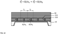
- FIG. 1A schematically shows an embodiment of a donor plate 1 for deposition of a deposition substance 2 on a target 30.
- the donor plate comprises a flexible substrate 10, e.g. a silicon substrate, which at a first main surface 101 subsequently has an electrode layer 11, a first electrically insulating layer 12, a resistive heater layer 13, a second electrically insulating layer 14 and a patterned layer 15 provided with one or more recesses 155 for holding deposition substance 2 to be deposited on the target.
- the patterned layer 15 may comprise a thermal insulator layer 21 to reduce a heat flux outside the areas defined by the recesses.
- the electrode layer 11 comprises a first and a second electrode 111, 112 which are of a complementary shape and which are electrically insulated from each other by a gap 113.
- the gap may be provided as free space or may be filled with an insulating material.
- a width Wg of the gap is less than 10 micron, e.g. less than 3 micron.
- the resistive heater layer 13 is electrically connected to each of a contact surface of the first electrode 111 and a contact surface of the second electrode 112 via at least one respective slit 121, 122 in the first electrically insulating layer.
- the slits have a width Ws of less than 3 micron.
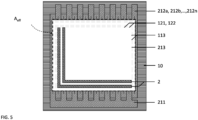
- the first and the second electrode 111, 112 are comb-shaped. Each of the electrodes has a respective sets of comb fingers 1111, 1121. As can be seen in FIG. 2 , the comb fingers 1111 of the first electrode 111 and the comb fingers 1121 of the second electrode 112 are interleaved.
- the at least one slit 121 of the first electrode 111 comprises a respective slit for each comb finger 1111 of the first electrode 111 and the at least one slit 122 of the second electrode 112 comprises a respective slit for each comb finger 1121 of the second electrode 112.
- the slits in the first electrically insulating layer 12 extend in a longitudinal direction of the comb fingers over their respective contact surface 1112, 1122.
- the distance De between the slits is smaller than about 2 mm.
- the smallest distance De between the at least one slit 121 of the first electrode 111 and the least one slit 122 of the second electrode 112 is at most one tenth of the square root of an effective surface area A eff of the resistive heater layer 13.
- the effective surface area A eff of the resistive heater layer 13 referred to herein is the area of the resistive heater layer that is electrically connected with both electrodes. In the example shown, the effective surface area A eff is equal to the product of a length L and a width W of the resistive heater layer 13 that is in electric contact with the electrodes 111, 112.
- the values for the length L and the width W may both be 3 cm, and therewith the distance De between the slits is less than one tenth of the square root of the effective surface area Aeff of the resistive heater layer.
- FIG. 1B shows a heatflux as measured as a function of a position in a direction from left to right along a surface of the resistive heater layer 13 facing the patterned layer 15
- the arrangement of the resistive heater layer of FIG. 1A and 2 provides for a very homogeneous heat flow, so that the deposition substance is ejected with a uniform ejection velocity within a recess 155. Only minor variations occur. I.e. at the location of the slit 122 small dips occur in the heatflux towards the patterned layer.
- FIG. 1B shows that the magnitude of the heatflux is slightly above the threshold heatflux The required to eject the deposition substance 2 out of the recesses.
- ⁇ ⁇ 1 and ⁇ ⁇ 2 are the sheet resistance of a portion of the resistive heater layer 13 between the first pair of subsequent slits and between the second pair of subsequent slits respectively.
- the portions may have a mutually different sheet resistance by an appropriate selection of the resistive material for the resistive heater layer portions or by an appropriate selection of their thicknesses.
- FIG. 3A, 3B and 3C schematically shows three operational stages of a deposition device.
- the deposition device comprises a donor plate 1 and a plate carrier 16.
- the donor plate 1 is laterally attached at a second main surface 102 opposite its first main surface 101 to a first plate carrier surface 161 of the plate carrier 16.
- the plate carrier 16 is mounted to a reference frame REF at a first side 163. At a second side 164 opposite the first side it is slidably coupled to the reference frame to allow the plate carrier 16 to expand in a direction along an axis from the first side to the second side.
- the donor plate 1 is fixed to the plate carrier 16 with a round going seal 165 and the plate carrier has one or more channels 166 extending through the plate carrier, which channels 166 are configured to be coupled to a pressure control unit.
- the deposition device shown in this example comprises one or more spacers 151 at a free surface 17 of the patterned layer 15.
- the donor plate 1 is positioned with its patterned layer 15 in a non-contacting manner in front of the target 30. It can be seen that the spacers 151 therewith maintain a predetermined distance of the patterned layer 15 to the target surface. Alternatively a servo system may be used to achieve a proper positioning.
- the donor plate typically has a temperature equal to roomtemperature, e.g. about 20°C.
- a subsequent step S2 an electric voltage is applied to the resistive heater layer 13 of the donor plate to therewith heat the donor plate in a substantially uniform manner.
- the first main surface 101 which is closer to the patterned surface is heated more rapidly than the second main surface 102, facing the plate carrier 16 a substantial temperature difference is caused.
- the second main surface 102 still has a temperature close to room temperature
- the first main surface 101 may rapidly achieve, for example within 5 to 15 microsecond, a substantially higher temperature in the order of magnitude of a few hundred degrees, e.g. 500°C.
- the donor plate is deformed over a width Wd until the patterned layer 15 contacts the target.
- the deposition substance is ejected in step S3 to be deposited from the recesses 151 onto the target.
- the traveling distance for the deposition substance is substantially zero, so that lateral deviations in the deposition location are minimized.
- the donor plate is cooled down so that the patterned layer 15 is retracted away from the target. Also the retraction can take place rapidly, for example in 20 to 40 microseconds, e.g. in a time frame of 30 microseconds the plate is cooled down to a uniform temperature of a few tens of degrees e.g. 40oC and fully retracted to the plate carrier 16.
- the ejection of the deposition substance 2 is initiated by the step of resistively heating.
- the rapid retraction of the donor plate 1 contributes to a better release of the deposition substance 2.
- the donor plate 1 has retracted away from the target 30 over a distance PG.
- the distance PG maybe a fraction of the print thickness PT, i.e. the dept of the recesses in the patterned surface of the plate, e.g. PG is about 1/3 to 1 ⁇ 2 of the print thickness PT.
- retraction is relatively slow, e.g. has taken a few milliseconds, e.g. 10 milliseconds. In this timeframe the deposition substance 2a, could flow out, therewith contact the edges of the recess from which it was ejected, and stick thereto after solidification.
- FIG. 4B shows the situation wherein retraction has taken place in a few microseconds to a few tens of microseconds, e.g. in 10 microseconds. In this timeframe the deposition substance 2b does not have sufficient time to flow out, so that is avoided that it sticks to the donor plate after ejection.
- a donor plate as shown in FIG. 5 that has respective, independently controllable sets of one or more resistive heating elements arranged between the second electrically insulating layer 14 and the patterned layer 15 in respective zones defined by respective ones of the recesses.
- the donor plate may be heated in step S2 at its first main surface 101 to a temperature that is sufficiently high to deform the plate, and in step S3, the ejection of deposition substance 2 can be accurately controlled by selectively providing electric energy to a specific selected control electrode 212a, 212b, ...212n of a set of one or more dedicated resistive heating elements.
- the resistive heating elements may share a common second electrode 211. Therewith the timing of the ejection can be controlled independently from the timing of the deformation of the plate.
- ejection of the deposition substance 2 can be controlled to take place in a particular state of the donor plate 1.
- the velocity with which the deposition substance 2 is ejected in step S3 can be increased by timing the ejection when the donor plate 1 is moving towards the target 30.
- the velocity of the donor plate 1 in the direction of the target 30 induced in step S2 as a result of its thermal expansion is 10 m/s and that the deposition substance 2 is ejected from the donor plate 1 with a velocity of 10 m/s by energizing one or more of the dedicated resistive heating elements, then the deposition substance 2 will be transferred with a velocity of 20 m/s towards the target 30.
- the deposition substance 2 is ejected at 10 m/s while the donor plate 1 is retracting at 10 m/s then the resulting velocity is 0 m/s, which makes gravity causing the deposition substance to fall onto the target 30.
- This reduced impact speed could be beneficial for preventing lower viscous deposition substances to splash, or making it possible to wrap ink around surfaces without breaking up due to high shear forces.
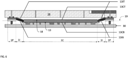
- FIG. 6 shows an example of the deposition device wherein the donor plate 1 in a radially outward direction has a central section 1C, a resistively heatable intermediary section 1I and a peripheral section 1P.
- the central section 1C comprises a section of the flexible substrate 10, with the electrode layer 11, the first electrically insulating layer 12, the resistive heater layer 13, the second electrically insulating layer 14 and the patterned layer 15.
- the intermediate section 1I surrounds the central section 1C and the donor plate 1 is attached with its peripheral section 1P to the plate carrier 16.
- the central section 1C has mutually a bottom resistive heater layer 13CB and a top resistive heater layer 13CT which are arranged at mutually opposite sides of a neutral plane defined by the flexible substrate 10.
- the intermediary section 1I is also resistively heatable in that it has a bottom resistive heater layer 13IB and a top resistive heater layer 13IT .
- the central section 1C of the donor plate can be translated towards the target without substantial deformation.
- Deformation of the central section 1C is further mitigated in that the bottom resistive heater layer 13CB and the top resistive heater layer 13CT are controlled to avoid a substantial temperature gradient in the central section 1C in a direction of its surface normal.
- the intermediary section 1I may have a thermal expansion coefficient greater than that of the central section 1C, for example by a local modification of the substrate. Therewith a substantial deformation of the intermediary section 1I can be achieved.
- electrodes for supplying the resistive heaters 13CB, 13CT, 13IB, 13IT may be provided from copper an be embedded in a silicon substrate.
- Copper has a thermal expansion coefficient of about 17 ppm/K, while silicon is around 3.3 ppm/K. Moreover, copper has a very high thermal conductivity. This has the advantage that heating/cooling and therewith expansion and retraction of the plate can be achieved even more rapidly.
- FIG. 7A and 7B shows two further embodiments of a deposition device.
- the deposition plate 1 has a central section 1C with a thickness that increases in a radially outward direction. This is achieved in that the flexible substrate 10 of the plate has the radially increasing thickness.
- the central section 1C has a thickness that increases in a radially outward direction. However, in this embodiment this is achieved in that a coating 117 having a low thermal conductivity and having the appropriate thickness profile is applied on the second main surface 102 of the flexible substrate 10.
- the flexible substrate 10 proper is of uniform thickness in this case.
- the thermal equilibration time is relatively low in the center of the plate as compared to that in a more radially outward direction. As a result, a higher thermal expansion occurs in the periphery of the plate while the plate remains substantially flat in the printing area.
- thermal buffer layers e.g. from a ceramic material, such as SiO2 may be provided between the flexible substrate 10 and the resistive heater layer 13 to provide for a reduced heatflux into the substrate. Simulations were performed which are described below with reference to FIG. 8 , FIG. 9A, 9B, 9C and FIG. 10A, 10B .
- FIG. 8 schematically shows the simulated donor plate 1 for deposition of the substance 2, in this case an ink.
- the donor plate is provided with a silicon substrate 10 having a thickness of 300 micron.
- the substrate 10 is provided with a copper electrode layer 11 at its first main surface 101 (indicated by a dashed line).
- the electrode layer comprises a first electrode 111 and a second electrode 112 of a complementary shape having a thickness of 50 micron that are embedded in the silicon substrate at its first main surface 101 and that are electrically insulated from each other by the material of the substrate. It is noted that not all elements in the drawing are presented at the same scale. For example, for clarity only the upper portion of the substrate 10 is shown. More details about the dimensions and the material properties used for the simulation are provided in the table below.
- the simulated donor plate 1 comprises a first electrically insulating layer 12 of SiO2, a molybdenum resistive heater layer 13 a second electrically insulating layer 14 of Si3N4) and a patterned layer provided with one or more recesses 155 for holding the deposition substance 2 to be deposited.
- FIG. 8 only shows a portion where the simulated donor plate forms a recess 155 in the patterned layer.
- the resistive heater layer 13 is electrically connected to each of a contact surface of the first electrode 111 and a contact surface of the second electrode 112 via a respective slit 121, 122 in the first electrically insulating layer.
- FIG. 8 further shows a heat spreader layer 20 at a bottom of the recess 155.
- the heat spreader layer 20 is formed of tungsten and has a thickness of 1 micron.
- the simulation was performed with a fixed setting for the heat flux generated in the Mo layer of 150 kW/cm 2 .
- the thickness of the second insulating layer 14 and the dimensions of the slits 121, 121 were variable.
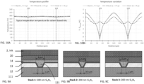
- FIG. 9A, 9B and 9C show three exemplary simulation settings denoted as Stack 1, Stack 2 and Stack 3 respectively.
- the slit tapers outward in a direction away from the first electrode 111 from a smallest width of 1 micron to a largest width of 2 micron, and the second insulating layer 14 has a thickness of 500 nm.
- the slit tapers outward in a direction away from the first electrode 111 from a smallest width of 0.5 micron to a largest width of 1.5 micron, and the second insulating layer 14 has a thickness of 200 nm.
- the slit tapers outward in a direction away from the first electrode 111 from a smallest width of 1 micron to a largest width of 2 micron, and the second insulating layer 14 has a thickness of 200 nm.
- the molybdenum layer 13 electrically contacts the first electrode 111 in the narrow part of the slit 121. The same applies to the electrical contact between the molybdenum layer 13 with the second electrode 112 in the slit 122. Because the electrical connections with the first and the second electrode are the same, only the electrical connection with the first electrode is shown.
- FIG. 10A, 10B shows a temperature distribution in the substance for each of these cases as a function of the position from left to right in the drawing.
- the positions of the slits 121, 122 are indicated.
- FIG. 10A shows the absolute value of the temperature
- FIG. 10B shows the deviation of the temperature from the average temperature.
- the temperature distribution of Stack 1 is determined after 6 microseconds and the temperature distribution of Stacks 2 and 3 is determined after 5 microseconds.
- the temperature distribution of Stacks 1 and 3 closely resemble each other.
- the temperature distribution of Stack 2 is more uniform as compared to Stacks 1 and 3. This is explained in that the contact area of the resistive layer 13 with the electrode 111, wherein the resistive layer does not generate heat, is substantially smaller in Stack 2 than in each of Stacks 1 and 3.
- the temperature above the slits 121, 122 achieves a maximum value that is almost equal to the average temperature.
- a relatively large surface is provided relative to the projection of this surface in the recess 155.
- the heat flux, the power per unit area, in the projection of the sidewall surface is higher than the heat flux generated in the side walls.
- the heat flux generated in the side walls of the resistive layer is larger than the heat flux generated in the areas of the resistive layer between the slits.
- the material for deposition is distributed on the sidewalls over a larger area than in the areas of the resistive layer between the slits. Therewith the thickness of the resistive layer at the sidewalls is less than the thickness of the resistive layer between the slits. Due the relatively high resistance of the resistive layer present on the sidewalls therein a relatively high heat flux is generated.
- the thickness of the first insulating layer 12 and the dimensions of the tapering slits 121, 122, i.e.
- the average heat flux in the projected area of the slit 121, 122 is approximately equal to the heat flux in the areas between the slits.
- the heat flux in the recess can be further homogenized by a heat distribution layer 20, as shown in FIG. 8 and 9A, 9B, 9C .
- the skilled person can therewith make a tradeoff between a desired extent of homogeneity and an efficiency of the device. If a high extent of homogeneity is desired, a relatively thick heat distribution layer 20 may be selected at the cost of some loss of efficiency, in that a longer heating time and more energy is required to obtain a desired average temperature. Accordingly, if the efficiency is more important, a thinner heat distribution layer 20 may be chosen.
Landscapes
- Engineering & Computer Science (AREA)
- Microelectronics & Electronic Packaging (AREA)
- Manufacturing & Machinery (AREA)
- Surface Heating Bodies (AREA)
- Physical Vapour Deposition (AREA)
- Chemical & Material Sciences (AREA)
- Dispersion Chemistry (AREA)
- Manufacturing Of Printed Wiring (AREA)
- Resistance Heating (AREA)
Claims (17)
- Donatorplatte (1) zur Abscheidung einer Abscheidungssubstanz (2) auf einem Target (30), wobei die Donatorplatte ein flexibles Substrat (10) umfasst, das an einer ersten Hauptfläche (101) eine strukturierte Schicht (15) aufweist, die mit einer oder mehreren Ausnehmungen (155) zum Halten der auf dem Target abzuscheidenden Abscheidungssubstanz (2) versehen ist,
dadurch gekennzeichnet, dass das flexible Substrat (10) an der ersten Hauptfläche (101) anschließend eine Elektrodenschicht (11), eine erste elektrisch isolierende Schicht (12), eine Widerstandsheizungsschicht (13), eine zweite elektrisch isolierende Schicht (14) und die strukturierte Schicht aufweist, wobei die Elektrodenschicht (11) eine erste und eine zweite Elektrode (111, 112) mit einer komplementären Form umfasst, die voneinander elektrisch isoliert sind, und wobei die Widerstandsheizungsschicht (13) über mindestens einen jeweiligen Schlitz (121, 122) in der ersten elektrisch isolierenden Schicht mit einer Kontaktfläche der ersten Elektrode (111) und einer Kontaktfläche der zweiten Elektrode (112) elektrisch verbunden ist. - Donatorplatte (1) nach Anspruch 1, wobei an jeder Position der Widerstandsheizungsschicht (13) der kleinste Abstand zwischen dem mindestens einen Schlitz (121) der ersten Elektrode (111) und dem mindestens einen Schlitz (122) der zweiten Elektrode (112) höchstens ein Zehntel der Quadratwurzel einer effektiven Oberfläche der Widerstandsheizungsschicht (13) beträgt.
- Donatorplatte (1) nach Anspruch 2, wobei die erste und die zweite Elektrode (111, 112) kammförmig sind und jeweilige Sätze von Kammfingern (1111, 1121) aufweisen, wobei die Kammfinger (1111) der ersten Elektrode (111) und die Kammfinger (1121) der zweiten Elektrode (112) ineinander verschachtelt sind, und wobei der mindestens eine Schlitz (121) der ersten Elektrode (111) einen entsprechenden Schlitz für jeden Kammfinger (1111) der ersten Elektrode (111) umfasst und wobei der mindestens eine Schlitz (122) der zweiten Elektrode (112) einen jeweiligen Schlitz für jeden Kammfinger (1121) der zweiten Elektrode (112) umfasst, wobei sich die jeweiligen Schlitze in der ersten elektrisch isolierenden Schicht (12) in einer Längsrichtung der Kammfinger über ihre jeweilige Kontaktfläche (1112, 1122) erstrecken.
- Donatorplatte (1) nach Anspruch 2, wobei sich die erste und die zweite Elektrode (111, 112) entlang einer spiralförmigen Bahn nebeneinander erstrecken, und wobei sich der mindestens eine erste Schlitz (121) in Längsrichtung über die Kontaktfläche der ersten Elektrode (111) und der mindestens eine zweite Schlitz (122) in Längsrichtung über die Kontaktfläche der zweiten Elektrode (112) erstreckt.
- Donatorplatte (1) nach Anspruch 1, zusätzlich umfassend jeweilige, unabhängig steuerbare Sätze von einem oder mehreren Widerstandsheizelementen, die zwischen der zweiten elektrisch isolierenden Schicht (14) und der strukturierten Schicht (15) in jeweiligen Zonen angeordnet sind, die durch jeweilige Ausnehmungen (155) definiert sind.
- Donatorplatte (1) nach Anspruch 5, wobei mindestens ein unabhängig steuerbarer Satz von einem oder mehreren Widerstandsheizelementen mindestens zwei unabhängig steuerbare Widerstandsheizelemente umfasst.
- Abscheidungsvorrichtung, umfassend die Spenderplatte (1) nach einem der vorhergehenden Ansprüche und einen Plattenträger (16), wobei die Spenderplatte (1) seitlich an einer zweiten Hauptfläche (102) gegenüber ihrer ersten Hauptfläche (101) an einer ersten Plattenträgerfläche (161) des Plattenträgers (16) befestigt ist.
- Abscheidungsvorrichtung nach Anspruch 7, wobei der Plattenträger (16) an einer ersten Seite (163) an einem Referenzrahmen (REF) befestigt ist und an einer zweiten Seite (164), die der ersten Seite gegenüberliegt, verschiebbar mit dem Referenzrahmen gekoppelt ist, damit sich der Plattenträger (16) in einer Richtung entlang einer Achse von der ersten Seite zur zweiten Seite ausdehnen kann.
- Abscheidungsvorrichtung nach Anspruch 7 oder 8, wobei die Spenderplatte (1) mit einer Rundlaufdichtung (165) an dem Plattenträger (16) befestigt ist, wobei der Plattenträger einen oder mehrere Kanäle (166) aufweist, die sich durch den Plattenträger erstrecken, wobei die Kanäle (166) so konfiguriert sind, dass sie mit einer Drucksteuereinheit gekoppelt sind.
- Abscheidungsvorrichtung nach Anspruch 7, 8 oder 9, umfassend einen oder mehrere Abstandshalter (151) an einer freien Oberfläche (17) der strukturierten Schicht (15).
- Abscheidungsvorrichtung nach einem der Ansprüche 7 bis 10, wobei die Donatorplatte (1) in radialer Richtung nach außen einen Mittelabschnitt (1C), einen widerstandsbeheizbaren Zwischenabschnitt (1I) und einen peripheren Abschnitt (1P) aufweist, wobei der Mittelabschnitt einen Abschnitt des flexiblen Substrats (10) mit der Elektrodenschicht (11) umfasst, umfassend die erste elektrisch isolierende Schicht (12), die Widerstandsheizungsschicht (13), die zweite elektrisch isolierende Schicht (14) und die strukturierte Schicht (15), wobei der Zwischenabschnitt (1I) den Mittelabschnitt (1C) umgibt und wobei die Donatorplatte mit ihrem Umfangsabschnitt (1P) am Plattenträger (16) befestigt ist.
- Abscheidungsvorrichtung nach Anspruch 11, wobei der Zwischenabschnitt (1I) einen größeren Wärmeausdehnungskoeffizienten als der Mittelabschnitt (1C) aufweist.
- Abscheidungsvorrichtung nach Anspruch 11 oder 12, wobei der Zwischenabschnitt (1I) eine Vielzahl von Heizschichten umfasst.
- Abscheidungsvorrichtung nach Anspruch 11, 12 oder 13, wobei der Mittelabschnitt (1C) eine weitere Widerstandsheizungsschicht (18) umfasst, wobei die Widerstandsheizungsschicht (13) und die weitere Widerstandsheizungsschicht (18) an gegenüberliegenden Seiten einer virtuellen Mittelebene (19) des Mittelabschnitts (1C) angeordnet sind.
- Abscheidungsvorrichtung nach Anspruch 11, 12 oder 13, wobei die Dicke des Mittelabschnitts (1C) in radialer Richtung nach außen hin zunimmt.
- Verfahren zum Abscheiden unter Verwendung einer Donatorplatte (1), die ein flexibles Substrat (10) umfasst, das an einer ersten Hauptfläche (101) eine strukturierte Schicht (15) aufweist, die mit einer oder mehreren Ausnehmungen (151) zum Halten der auf einem Target (30) abzuscheidenden Abscheidungssubstanz (2) versehen ist, wobei das Verfahren umfasst:Positionieren (S1) der Donatorplatte mit ihrer strukturierten Schicht (15) berührungslos vor dem Target (30);im Wesentlichen gleichmäßiges Erwärmen (S2) der Donatorplatte;Ausstoßen (S3) der abzuscheidenden Abscheidungssubstanz aus den Vertiefungen (151) auf das TargetAbkühlen (S4) der Donatorplatte, um die strukturierte Schicht (15) vom Target zu entfernen,
dadurch gekennzeichnet, dass:das flexible Substrat (10) an der ersten Hauptfläche (101) anschließend eine Elektrodenschicht (11), eine erste elektrisch isolierende Schicht (12), eine Widerstandsheizungsschicht (13), eine zweite elektrisch isolierende Schicht (14) und die strukturierte Schicht (15) aufweist, wobei die Elektrodenschicht (11) eine erste und eine zweite Elektrode (111, 112) mit einer komplementären Form umfasst und elektrisch voneinander isoliert ist, und wobei die Widerstandsheizungsschicht (13) über mindestens einen jeweiligen Schlitz (121, 122) in der ersten elektrisch isolierenden Schicht mit einer Kontaktfläche der ersten Elektrode (111) und einer Kontaktfläche der zweiten Elektrode (112) elektrisch verbunden ist, und dadurch, dassdie Donatorplatte mit der Widerstandsheizungsschicht (13) im Wesentlichen gleichmäßig erwärmt wird (S2), um damit die Donatorplatte zu verformen, damit sich die strukturierte Schicht (15) zum Target hin bewegt. - Verfahren nach Anspruch 16, wobei die Donatorplatte jeweils unabhängig steuerbare Sätze von einem oder mehreren Widerstandsheizelementen aufweist, die zwischen der zweiten elektrisch isolierenden Schicht (14) und der strukturierten Schicht (15) in jeweiligen Zonen angeordnet sind, die durch jeweilige Ausnehmungen definiert sind, und wobei das Verfahren ferner die unabhängige Steuerung des Schritts des Ausstoßens (S3) durch Bereitstellung elektrischer Energie für die jeweiligen, unabhängig steuerbaren Sätze von einem oder mehreren Widerstandsheizelementen umfasst.
Applications Claiming Priority (2)
| Application Number | Priority Date | Filing Date | Title |
|---|---|---|---|
| EP21154587.6A EP4037442A1 (de) | 2021-02-01 | 2021-02-01 | Donorplatte, abscheidungsvorrichtung und abscheidungsverfahren |
| PCT/NL2022/050043 WO2022164320A1 (en) | 2021-02-01 | 2022-01-31 | Donor plate, deposition device and deposition method |
Publications (3)
| Publication Number | Publication Date |
|---|---|
| EP4285694A1 EP4285694A1 (de) | 2023-12-06 |
| EP4285694C0 EP4285694C0 (de) | 2025-05-14 |
| EP4285694B1 true EP4285694B1 (de) | 2025-05-14 |
Family
ID=74494818
Family Applications (2)
| Application Number | Title | Priority Date | Filing Date |
|---|---|---|---|
| EP21154587.6A Withdrawn EP4037442A1 (de) | 2021-02-01 | 2021-02-01 | Donorplatte, abscheidungsvorrichtung und abscheidungsverfahren |
| EP22702799.2A Active EP4285694B1 (de) | 2021-02-01 | 2022-01-31 | Donorplatte, abscheidungsvorrichtung und abscheidungsverfahren |
Family Applications Before (1)
| Application Number | Title | Priority Date | Filing Date |
|---|---|---|---|
| EP21154587.6A Withdrawn EP4037442A1 (de) | 2021-02-01 | 2021-02-01 | Donorplatte, abscheidungsvorrichtung und abscheidungsverfahren |
Country Status (6)
| Country | Link |
|---|---|
| US (1) | US20240314935A1 (de) |
| EP (2) | EP4037442A1 (de) |
| JP (1) | JP2024515924A (de) |
| KR (1) | KR20230135111A (de) |
| CN (1) | CN116941332A (de) |
| WO (1) | WO2022164320A1 (de) |
Families Citing this family (2)
| Publication number | Priority date | Publication date | Assignee | Title |
|---|---|---|---|---|
| EP4383321A1 (de) * | 2022-12-06 | 2024-06-12 | Nederlandse Organisatie voor toegepast-natuurwetenschappelijk Onderzoek TNO | Verfahren und vorrichtung zum abscheiden von bauelementen auf einem substrat |
| EP4586308A1 (de) | 2024-01-15 | 2025-07-16 | FononTech Holding B.V. | Abscheidungssystem und -verfahren |
Family Cites Families (9)
| Publication number | Priority date | Publication date | Assignee | Title |
|---|---|---|---|---|
| JPS61254350A (ja) * | 1985-05-08 | 1986-11-12 | Mitsubishi Electric Corp | サ−マルジエツト用記録ヘツド |
| US6114088A (en) * | 1999-01-15 | 2000-09-05 | 3M Innovative Properties Company | Thermal transfer element for forming multilayer devices |
| DE10240105B4 (de) * | 2002-08-30 | 2005-03-24 | Infineon Technologies Ag | Herstellung organischer elektronischer Schaltkreise durch Kontaktdrucktechniken |
| US8425974B2 (en) * | 2007-11-29 | 2013-04-23 | Semiconductor Energy Laboratory Co., Ltd. | Evaporation donor substrate and method for manufacturing light-emitting device |
| US20100118243A1 (en) * | 2008-11-12 | 2010-05-13 | Debasis Majumdar | Polymeric conductive donor and transfer method |
| WO2015128857A1 (en) | 2014-02-28 | 2015-09-03 | Utilight Ltd. | Tracks patterns production apparatus |
| JP6439432B2 (ja) * | 2014-12-18 | 2018-12-19 | 株式会社リコー | 定着装置及び画像形成装置 |
| EP3911130A1 (de) * | 2020-05-12 | 2021-11-17 | Nederlandse Organisatie voor toegepast- natuurwetenschappelijk Onderzoek TNO | Transfer von viskosen materialien |
| EP4586308A1 (de) * | 2024-01-15 | 2025-07-16 | FononTech Holding B.V. | Abscheidungssystem und -verfahren |
-
2021
- 2021-02-01 EP EP21154587.6A patent/EP4037442A1/de not_active Withdrawn
-
2022
- 2022-01-31 WO PCT/NL2022/050043 patent/WO2022164320A1/en not_active Ceased
- 2022-01-31 JP JP2023546316A patent/JP2024515924A/ja active Pending
- 2022-01-31 US US18/274,618 patent/US20240314935A1/en active Pending
- 2022-01-31 EP EP22702799.2A patent/EP4285694B1/de active Active
- 2022-01-31 KR KR1020237028044A patent/KR20230135111A/ko active Pending
- 2022-01-31 CN CN202280017200.0A patent/CN116941332A/zh active Pending
Also Published As
| Publication number | Publication date |
|---|---|
| JP2024515924A (ja) | 2024-04-11 |
| US20240314935A1 (en) | 2024-09-19 |
| EP4285694C0 (de) | 2025-05-14 |
| EP4285694A1 (de) | 2023-12-06 |
| EP4037442A1 (de) | 2022-08-03 |
| CN116941332A (zh) | 2023-10-24 |
| KR20230135111A (ko) | 2023-09-22 |
| WO2022164320A1 (en) | 2022-08-04 |
Similar Documents
| Publication | Publication Date | Title |
|---|---|---|
| EP4285694B1 (de) | Donorplatte, abscheidungsvorrichtung und abscheidungsverfahren | |
| US6805918B2 (en) | Laser forward transfer of rheological systems | |
| EP4151057B1 (de) | Transfer von viskosen materialien | |
| US20080268584A1 (en) | Electronic devices and methods for forming the same | |
| US5594488A (en) | Thermal head | |
| CN107535017A (zh) | 加热器、定影装置、图像形成装置以及加热装置 | |
| JP6926078B2 (ja) | 回路形成方法、および回路形成装置 | |
| US8998385B2 (en) | Thermal head, printer, and method of manufacturing thermal head | |
| JP3825047B2 (ja) | サーマルヘッドにおける共通電極パターンに対する補助電極層の形成方法 | |
| CN120731289A (zh) | 沉积装置、用于沉积的方法、用于将裸片封装在芯片封装件中的方法 | |
| WO2002092674A1 (en) | Laser forward transfer of rheological systems | |
| JP2000168028A (ja) | 凹版印刷装置および方法 | |
| EP3217773B1 (de) | Verdrahtungsherstellungsverfahren und leiterplatte | |
| US8730286B2 (en) | Thermal head manufacturing method, thermal head, and printer | |
| JPS61158474A (ja) | サ−マルヘツド | |
| JPH0517864B2 (de) | ||
| JP2021094715A (ja) | 3次元造形装置及び3次元造形装置用の造形ステージ | |
| JP2002002005A (ja) | 厚膜型サーマルプリントヘッド | |
| WO1992005404A1 (en) | True edge thermal printhead | |
| JPS6072752A (ja) | サ−マルヘツド | |
| JP2958496B2 (ja) | 厚膜型サーマルヘッドの製造方法 | |
| JPS5955042A (ja) | 液相を熱移動する方法および装置 | |
| KR20230008131A (ko) | 고점도 물질의 패턴 전사 | |
| JP3401144B2 (ja) | サーマルヘッド | |
| US12053929B2 (en) | Build units for three-dimensional printers |
Legal Events
| Date | Code | Title | Description |
|---|---|---|---|
| STAA | Information on the status of an ep patent application or granted ep patent |
Free format text: STATUS: UNKNOWN |
|
| STAA | Information on the status of an ep patent application or granted ep patent |
Free format text: STATUS: THE INTERNATIONAL PUBLICATION HAS BEEN MADE |
|
| PUAI | Public reference made under article 153(3) epc to a published international application that has entered the european phase |
Free format text: ORIGINAL CODE: 0009012 |
|
| STAA | Information on the status of an ep patent application or granted ep patent |
Free format text: STATUS: REQUEST FOR EXAMINATION WAS MADE |
|
| 17P | Request for examination filed |
Effective date: 20230814 |
|
| AK | Designated contracting states |
Kind code of ref document: A1 Designated state(s): AL AT BE BG CH CY CZ DE DK EE ES FI FR GB GR HR HU IE IS IT LI LT LU LV MC MK MT NL NO PL PT RO RS SE SI SK SM TR |
|
| DAV | Request for validation of the european patent (deleted) | ||
| DAX | Request for extension of the european patent (deleted) | ||
| STAA | Information on the status of an ep patent application or granted ep patent |
Free format text: STATUS: EXAMINATION IS IN PROGRESS |
|
| 17Q | First examination report despatched |
Effective date: 20240823 |
|
| GRAP | Despatch of communication of intention to grant a patent |
Free format text: ORIGINAL CODE: EPIDOSNIGR1 |
|
| STAA | Information on the status of an ep patent application or granted ep patent |
Free format text: STATUS: GRANT OF PATENT IS INTENDED |
|
| INTG | Intention to grant announced |
Effective date: 20241213 |
|
| GRAS | Grant fee paid |
Free format text: ORIGINAL CODE: EPIDOSNIGR3 |
|
| GRAA | (expected) grant |
Free format text: ORIGINAL CODE: 0009210 |
|
| STAA | Information on the status of an ep patent application or granted ep patent |
Free format text: STATUS: THE PATENT HAS BEEN GRANTED |
|
| AK | Designated contracting states |
Kind code of ref document: B1 Designated state(s): AL AT BE BG CH CY CZ DE DK EE ES FI FR GB GR HR HU IE IS IT LI LT LU LV MC MK MT NL NO PL PT RO RS SE SI SK SM TR |
|
| REG | Reference to a national code |
Ref country code: GB Ref legal event code: FG4D |
|
| REG | Reference to a national code |
Ref country code: CH Ref legal event code: EP |
|
| REG | Reference to a national code |
Ref country code: DE Ref legal event code: R096 Ref document number: 602022014635 Country of ref document: DE |
|
| REG | Reference to a national code |
Ref country code: IE Ref legal event code: FG4D |
|
| U01 | Request for unitary effect filed |
Effective date: 20250519 |
|
| U07 | Unitary effect registered |
Designated state(s): AT BE BG DE DK EE FI FR IT LT LU LV MT NL PT RO SE SI Effective date: 20250523 |
|
| PG25 | Lapsed in a contracting state [announced via postgrant information from national office to epo] |
Ref country code: ES Free format text: LAPSE BECAUSE OF FAILURE TO SUBMIT A TRANSLATION OF THE DESCRIPTION OR TO PAY THE FEE WITHIN THE PRESCRIBED TIME-LIMIT Effective date: 20250514 |
|
| PG25 | Lapsed in a contracting state [announced via postgrant information from national office to epo] |
Ref country code: NO Free format text: LAPSE BECAUSE OF FAILURE TO SUBMIT A TRANSLATION OF THE DESCRIPTION OR TO PAY THE FEE WITHIN THE PRESCRIBED TIME-LIMIT Effective date: 20250814 Ref country code: GR Free format text: LAPSE BECAUSE OF FAILURE TO SUBMIT A TRANSLATION OF THE DESCRIPTION OR TO PAY THE FEE WITHIN THE PRESCRIBED TIME-LIMIT Effective date: 20250815 |
|
| PG25 | Lapsed in a contracting state [announced via postgrant information from national office to epo] |
Ref country code: PL Free format text: LAPSE BECAUSE OF FAILURE TO SUBMIT A TRANSLATION OF THE DESCRIPTION OR TO PAY THE FEE WITHIN THE PRESCRIBED TIME-LIMIT Effective date: 20250514 |
|
| PG25 | Lapsed in a contracting state [announced via postgrant information from national office to epo] |
Ref country code: HR Free format text: LAPSE BECAUSE OF FAILURE TO SUBMIT A TRANSLATION OF THE DESCRIPTION OR TO PAY THE FEE WITHIN THE PRESCRIBED TIME-LIMIT Effective date: 20250514 |
|
| PG25 | Lapsed in a contracting state [announced via postgrant information from national office to epo] |
Ref country code: RS Free format text: LAPSE BECAUSE OF FAILURE TO SUBMIT A TRANSLATION OF THE DESCRIPTION OR TO PAY THE FEE WITHIN THE PRESCRIBED TIME-LIMIT Effective date: 20250814 |
|
| PG25 | Lapsed in a contracting state [announced via postgrant information from national office to epo] |
Ref country code: IS Free format text: LAPSE BECAUSE OF FAILURE TO SUBMIT A TRANSLATION OF THE DESCRIPTION OR TO PAY THE FEE WITHIN THE PRESCRIBED TIME-LIMIT Effective date: 20250914 |
|
| REG | Reference to a national code |
Ref country code: CH Ref legal event code: W10 Free format text: ST27 STATUS EVENT CODE: U-0-0-W10-W00 (AS PROVIDED BY THE NATIONAL OFFICE) Effective date: 20251224 |
|
| PG25 | Lapsed in a contracting state [announced via postgrant information from national office to epo] |
Ref country code: SM Free format text: LAPSE BECAUSE OF FAILURE TO SUBMIT A TRANSLATION OF THE DESCRIPTION OR TO PAY THE FEE WITHIN THE PRESCRIBED TIME-LIMIT Effective date: 20250514 |
|
| PG25 | Lapsed in a contracting state [announced via postgrant information from national office to epo] |
Ref country code: CZ Free format text: LAPSE BECAUSE OF FAILURE TO SUBMIT A TRANSLATION OF THE DESCRIPTION OR TO PAY THE FEE WITHIN THE PRESCRIBED TIME-LIMIT Effective date: 20250514 |
|
| RAP4 | Party data changed (patent owner data changed or rights of a patent transferred) |
Owner name: NEDERLANDSE ORGANISATIE VOOR TOEGEPAST-NATUURWETENSCHAPPELIJK ONDERZOEK TNO |
|
| U1H | Name or address of the proprietor changed after the registration of the unitary effect |
Owner name: NEDERLANDSE ORGANISATIE VOOR TOEGEPAST-NATUURWETENSCHAPPELIJK ONDERZOEK TNO; NL |
|
| PG25 | Lapsed in a contracting state [announced via postgrant information from national office to epo] |
Ref country code: SK Free format text: LAPSE BECAUSE OF FAILURE TO SUBMIT A TRANSLATION OF THE DESCRIPTION OR TO PAY THE FEE WITHIN THE PRESCRIBED TIME-LIMIT Effective date: 20250514 |
|
| U20 | Renewal fee for the european patent with unitary effect paid |
Year of fee payment: 5 Effective date: 20260129 |
|
| PLBE | No opposition filed within time limit |
Free format text: ORIGINAL CODE: 0009261 |
|
| STAA | Information on the status of an ep patent application or granted ep patent |
Free format text: STATUS: NO OPPOSITION FILED WITHIN TIME LIMIT |
|
| REG | Reference to a national code |
Ref country code: CH Ref legal event code: L10 Free format text: ST27 STATUS EVENT CODE: U-0-0-L10-L00 (AS PROVIDED BY THE NATIONAL OFFICE) Effective date: 20260325 |
|
| PGFP | Annual fee paid to national office [announced via postgrant information from national office to epo] |
Ref country code: GB Payment date: 20260123 Year of fee payment: 5 |
|
| 26N | No opposition filed |
Effective date: 20260217 |