EP4220734B1 - Wide band gap transistor with nanolaminated insulating gate strutcture and process for manufacturing a wide band gap transistor - Google Patents
Wide band gap transistor with nanolaminated insulating gate strutcture and process for manufacturing a wide band gap transistor Download PDFInfo
- Publication number
- EP4220734B1 EP4220734B1 EP23152421.6A EP23152421A EP4220734B1 EP 4220734 B1 EP4220734 B1 EP 4220734B1 EP 23152421 A EP23152421 A EP 23152421A EP 4220734 B1 EP4220734 B1 EP 4220734B1
- Authority
- EP
- European Patent Office
- Prior art keywords
- insulating gate
- forming
- gate structure
- aluminum
- layer
- Prior art date
- Legal status (The legal status is an assumption and is not a legal conclusion. Google has not performed a legal analysis and makes no representation as to the accuracy of the status listed.)
- Active
Links
Images




Classifications
-
- H—ELECTRICITY
- H10—SEMICONDUCTOR DEVICES; ELECTRIC SOLID-STATE DEVICES NOT OTHERWISE PROVIDED FOR
- H10D—INORGANIC ELECTRIC SEMICONDUCTOR DEVICES
- H10D30/00—Field-effect transistors [FET]
- H10D30/60—Insulated-gate field-effect transistors [IGFET]
- H10D30/64—Double-diffused metal-oxide semiconductor [DMOS] FETs
- H10D30/66—Vertical DMOS [VDMOS] FETs
-
- H—ELECTRICITY
- H10—SEMICONDUCTOR DEVICES; ELECTRIC SOLID-STATE DEVICES NOT OTHERWISE PROVIDED FOR
- H10D—INORGANIC ELECTRIC SEMICONDUCTOR DEVICES
- H10D30/00—Field-effect transistors [FET]
- H10D30/01—Manufacture or treatment
- H10D30/015—Manufacture or treatment of FETs having heterojunction interface channels or heterojunction gate electrodes, e.g. HEMT
-
- H—ELECTRICITY
- H10—SEMICONDUCTOR DEVICES; ELECTRIC SOLID-STATE DEVICES NOT OTHERWISE PROVIDED FOR
- H10D—INORGANIC ELECTRIC SEMICONDUCTOR DEVICES
- H10D30/00—Field-effect transistors [FET]
- H10D30/01—Manufacture or treatment
- H10D30/021—Manufacture or treatment of FETs having insulated gates [IGFET]
- H10D30/028—Manufacture or treatment of FETs having insulated gates [IGFET] of double-diffused metal oxide semiconductor [DMOS] FETs
- H10D30/0291—Manufacture or treatment of FETs having insulated gates [IGFET] of double-diffused metal oxide semiconductor [DMOS] FETs of vertical DMOS [VDMOS] FETs
-
- H—ELECTRICITY
- H10—SEMICONDUCTOR DEVICES; ELECTRIC SOLID-STATE DEVICES NOT OTHERWISE PROVIDED FOR
- H10D—INORGANIC ELECTRIC SEMICONDUCTOR DEVICES
- H10D30/00—Field-effect transistors [FET]
- H10D30/40—FETs having zero-dimensional [0D], one-dimensional [1D] or two-dimensional [2D] charge carrier gas channels
- H10D30/47—FETs having zero-dimensional [0D], one-dimensional [1D] or two-dimensional [2D] charge carrier gas channels having two-dimensional [2D] charge carrier gas channels, e.g. nanoribbon FETs or high electron mobility transistors [HEMT]
- H10D30/471—High electron mobility transistors [HEMT] or high hole mobility transistors [HHMT]
- H10D30/475—High electron mobility transistors [HEMT] or high hole mobility transistors [HHMT] having wider bandgap layer formed on top of lower bandgap active layer, e.g. undoped barrier HEMTs such as i-AlGaN/GaN HEMTs
-
- H—ELECTRICITY
- H10—SEMICONDUCTOR DEVICES; ELECTRIC SOLID-STATE DEVICES NOT OTHERWISE PROVIDED FOR
- H10D—INORGANIC ELECTRIC SEMICONDUCTOR DEVICES
- H10D62/00—Semiconductor bodies, or regions thereof, of devices having potential barriers
- H10D62/80—Semiconductor bodies, or regions thereof, of devices having potential barriers characterised by the materials
- H10D62/82—Heterojunctions
- H10D62/824—Heterojunctions comprising only Group III-V materials heterojunctions, e.g. GaN/AlGaN heterojunctions
-
- H—ELECTRICITY
- H10—SEMICONDUCTOR DEVICES; ELECTRIC SOLID-STATE DEVICES NOT OTHERWISE PROVIDED FOR
- H10D—INORGANIC ELECTRIC SEMICONDUCTOR DEVICES
- H10D62/00—Semiconductor bodies, or regions thereof, of devices having potential barriers
- H10D62/80—Semiconductor bodies, or regions thereof, of devices having potential barriers characterised by the materials
- H10D62/83—Semiconductor bodies, or regions thereof, of devices having potential barriers characterised by the materials being Group IV materials, e.g. B-doped Si or undoped Ge
- H10D62/832—Semiconductor bodies, or regions thereof, of devices having potential barriers characterised by the materials being Group IV materials, e.g. B-doped Si or undoped Ge being Group IV materials comprising two or more elements, e.g. SiGe
- H10D62/8325—Silicon carbide
-
- H—ELECTRICITY
- H10—SEMICONDUCTOR DEVICES; ELECTRIC SOLID-STATE DEVICES NOT OTHERWISE PROVIDED FOR
- H10D—INORGANIC ELECTRIC SEMICONDUCTOR DEVICES
- H10D62/00—Semiconductor bodies, or regions thereof, of devices having potential barriers
- H10D62/80—Semiconductor bodies, or regions thereof, of devices having potential barriers characterised by the materials
- H10D62/85—Semiconductor bodies, or regions thereof, of devices having potential barriers characterised by the materials being Group III-V materials, e.g. GaAs
- H10D62/8503—Nitride Group III-V materials, e.g. AlN or GaN
-
- H—ELECTRICITY
- H10—SEMICONDUCTOR DEVICES; ELECTRIC SOLID-STATE DEVICES NOT OTHERWISE PROVIDED FOR
- H10D—INORGANIC ELECTRIC SEMICONDUCTOR DEVICES
- H10D64/00—Electrodes of devices having potential barriers
- H10D64/01—Manufacture or treatment
- H10D64/013—Manufacture or treatment of electrodes having a conductor capacitively coupled to a semiconductor by an insulator
- H10D64/01302—Manufacture or treatment of electrodes having a conductor capacitively coupled to a semiconductor by an insulator the insulator being formed after the semiconductor body, the semiconductor being silicon
- H10D64/01332—Making the insulator
- H10D64/01336—Making the insulator on single crystalline silicon, e.g. chemical oxidation using a liquid
- H10D64/0134—Making the insulator on single crystalline silicon, e.g. chemical oxidation using a liquid with a treatment, e.g. annealing, after the formation of the insulator and before the formation of the conductor
-
- H—ELECTRICITY
- H10—SEMICONDUCTOR DEVICES; ELECTRIC SOLID-STATE DEVICES NOT OTHERWISE PROVIDED FOR
- H10D—INORGANIC ELECTRIC SEMICONDUCTOR DEVICES
- H10D64/00—Electrodes of devices having potential barriers
- H10D64/01—Manufacture or treatment
- H10D64/013—Manufacture or treatment of electrodes having a conductor capacitively coupled to a semiconductor by an insulator
- H10D64/01358—Manufacture or treatment of electrodes having a conductor capacitively coupled to a semiconductor by an insulator the insulator being formed after the semiconductor body, the semiconductor being a Group III-V material
-
- H—ELECTRICITY
- H10—SEMICONDUCTOR DEVICES; ELECTRIC SOLID-STATE DEVICES NOT OTHERWISE PROVIDED FOR
- H10D—INORGANIC ELECTRIC SEMICONDUCTOR DEVICES
- H10D64/00—Electrodes of devices having potential barriers
- H10D64/01—Manufacture or treatment
- H10D64/013—Manufacture or treatment of electrodes having a conductor capacitively coupled to a semiconductor by an insulator
- H10D64/01366—Manufacture or treatment of electrodes having a conductor capacitively coupled to a semiconductor by an insulator the semiconductor being silicon carbide
-
- H—ELECTRICITY
- H10—SEMICONDUCTOR DEVICES; ELECTRIC SOLID-STATE DEVICES NOT OTHERWISE PROVIDED FOR
- H10D—INORGANIC ELECTRIC SEMICONDUCTOR DEVICES
- H10D64/00—Electrodes of devices having potential barriers
- H10D64/60—Electrodes characterised by their materials
- H10D64/66—Electrodes having a conductor capacitively coupled to a semiconductor by an insulator, e.g. MIS electrodes
- H10D64/68—Electrodes having a conductor capacitively coupled to a semiconductor by an insulator, e.g. MIS electrodes characterised by the insulator, e.g. by the gate insulator
- H10D64/691—Electrodes having a conductor capacitively coupled to a semiconductor by an insulator, e.g. MIS electrodes characterised by the insulator, e.g. by the gate insulator comprising metallic compounds, e.g. metal oxides or metal silicates
-
- H—ELECTRICITY
- H10—SEMICONDUCTOR DEVICES; ELECTRIC SOLID-STATE DEVICES NOT OTHERWISE PROVIDED FOR
- H10P—GENERIC PROCESSES OR APPARATUS FOR THE MANUFACTURE OR TREATMENT OF DEVICES COVERED BY CLASS H10
- H10P14/00—Formation of materials, e.g. in the shape of layers or pillars
- H10P14/60—Formation of materials, e.g. in the shape of layers or pillars of insulating materials
- H10P14/63—Formation of materials, e.g. in the shape of layers or pillars of insulating materials characterised by the formation processes
- H10P14/6326—Deposition processes
- H10P14/6328—Deposition from the gas or vapour phase
- H10P14/6334—Deposition from the gas or vapour phase using decomposition or reaction of gaseous or vapour phase compounds, i.e. chemical vapour deposition
- H10P14/6339—Deposition from the gas or vapour phase using decomposition or reaction of gaseous or vapour phase compounds, i.e. chemical vapour deposition deposition by cyclic CVD, e.g. ALD, ALE or pulsed CVD
-
- H—ELECTRICITY
- H10—SEMICONDUCTOR DEVICES; ELECTRIC SOLID-STATE DEVICES NOT OTHERWISE PROVIDED FOR
- H10P—GENERIC PROCESSES OR APPARATUS FOR THE MANUFACTURE OR TREATMENT OF DEVICES COVERED BY CLASS H10
- H10P14/00—Formation of materials, e.g. in the shape of layers or pillars
- H10P14/60—Formation of materials, e.g. in the shape of layers or pillars of insulating materials
- H10P14/66—Formation of materials, e.g. in the shape of layers or pillars of insulating materials characterised by the type of materials
- H10P14/662—Laminate layers, e.g. stacks of alternating high-k metal oxides
-
- H—ELECTRICITY
- H10—SEMICONDUCTOR DEVICES; ELECTRIC SOLID-STATE DEVICES NOT OTHERWISE PROVIDED FOR
- H10P—GENERIC PROCESSES OR APPARATUS FOR THE MANUFACTURE OR TREATMENT OF DEVICES COVERED BY CLASS H10
- H10P14/00—Formation of materials, e.g. in the shape of layers or pillars
- H10P14/60—Formation of materials, e.g. in the shape of layers or pillars of insulating materials
- H10P14/69—Inorganic materials
- H10P14/692—Inorganic materials composed of oxides, glassy oxides or oxide-based glasses
- H10P14/6938—Inorganic materials composed of oxides, glassy oxides or oxide-based glasses the material containing at least one metal element, e.g. metal oxides, metal oxynitrides or metal oxycarbides
- H10P14/6939—Inorganic materials composed of oxides, glassy oxides or oxide-based glasses the material containing at least one metal element, e.g. metal oxides, metal oxynitrides or metal oxycarbides characterised by the metal
- H10P14/69391—Inorganic materials composed of oxides, glassy oxides or oxide-based glasses the material containing at least one metal element, e.g. metal oxides, metal oxynitrides or metal oxycarbides characterised by the metal the material containing aluminium, e.g. Al2O3
-
- H—ELECTRICITY
- H10—SEMICONDUCTOR DEVICES; ELECTRIC SOLID-STATE DEVICES NOT OTHERWISE PROVIDED FOR
- H10P—GENERIC PROCESSES OR APPARATUS FOR THE MANUFACTURE OR TREATMENT OF DEVICES COVERED BY CLASS H10
- H10P14/00—Formation of materials, e.g. in the shape of layers or pillars
- H10P14/60—Formation of materials, e.g. in the shape of layers or pillars of insulating materials
- H10P14/69—Inorganic materials
- H10P14/692—Inorganic materials composed of oxides, glassy oxides or oxide-based glasses
- H10P14/6938—Inorganic materials composed of oxides, glassy oxides or oxide-based glasses the material containing at least one metal element, e.g. metal oxides, metal oxynitrides or metal oxycarbides
- H10P14/6939—Inorganic materials composed of oxides, glassy oxides or oxide-based glasses the material containing at least one metal element, e.g. metal oxides, metal oxynitrides or metal oxycarbides characterised by the metal
- H10P14/69392—Inorganic materials composed of oxides, glassy oxides or oxide-based glasses the material containing at least one metal element, e.g. metal oxides, metal oxynitrides or metal oxycarbides characterised by the metal the material containing hafnium, e.g. HfO2
-
- H—ELECTRICITY
- H10—SEMICONDUCTOR DEVICES; ELECTRIC SOLID-STATE DEVICES NOT OTHERWISE PROVIDED FOR
- H10D—INORGANIC ELECTRIC SEMICONDUCTOR DEVICES
- H10D12/00—Bipolar devices controlled by the field effect, e.g. insulated-gate bipolar transistors [IGBT]
- H10D12/01—Manufacture or treatment
- H10D12/031—Manufacture or treatment of IGBTs
-
- H—ELECTRICITY
- H10—SEMICONDUCTOR DEVICES; ELECTRIC SOLID-STATE DEVICES NOT OTHERWISE PROVIDED FOR
- H10D—INORGANIC ELECTRIC SEMICONDUCTOR DEVICES
- H10D64/00—Electrodes of devices having potential barriers
- H10D64/20—Electrodes characterised by their shapes, relative sizes or dispositions
- H10D64/27—Electrodes not carrying the current to be rectified, amplified, oscillated or switched, e.g. gates
- H10D64/311—Gate electrodes for field-effect devices
- H10D64/411—Gate electrodes for field-effect devices for FETs
- H10D64/511—Gate electrodes for field-effect devices for FETs for IGFETs
- H10D64/512—Disposition of the gate electrodes, e.g. buried gates
- H10D64/513—Disposition of the gate electrodes, e.g. buried gates within recesses in the substrate, e.g. trench gates, groove gates or buried gates
-
- H—ELECTRICITY
- H10—SEMICONDUCTOR DEVICES; ELECTRIC SOLID-STATE DEVICES NOT OTHERWISE PROVIDED FOR
- H10D—INORGANIC ELECTRIC SEMICONDUCTOR DEVICES
- H10D64/00—Electrodes of devices having potential barriers
- H10D64/60—Electrodes characterised by their materials
- H10D64/66—Electrodes having a conductor capacitively coupled to a semiconductor by an insulator, e.g. MIS electrodes
- H10D64/68—Electrodes having a conductor capacitively coupled to a semiconductor by an insulator, e.g. MIS electrodes characterised by the insulator, e.g. by the gate insulator
- H10D64/681—Electrodes having a conductor capacitively coupled to a semiconductor by an insulator, e.g. MIS electrodes characterised by the insulator, e.g. by the gate insulator having a compositional variation, e.g. multilayered
- H10D64/685—Electrodes having a conductor capacitively coupled to a semiconductor by an insulator, e.g. MIS electrodes characterised by the insulator, e.g. by the gate insulator having a compositional variation, e.g. multilayered being perpendicular to the channel plane
Definitions
- the present invention relates to a wide band gap transistor with nanolaminated insulating gate structure and to a process for manufacturing a wide band gap transistor.
- semiconductor materials which have a Wide Band Gap (WBG), in particular, which have an energy value Eg of the band gap being greater than 1.1 eV, low on-state resistance (RON), a high value of thermal conductivity, high operating frequency and high saturation velocity of charge carriers, are particularly suitable for producing electronic components for power applications, such as MOSFET, JFET, HEMT (High Electron Mobility Transistors) and MISHEMT (Metal-Insulator-Semiconductor High Electron-Mobility Transistors).
- WBG Wide Band Gap
- Eg of the band gap being greater than 1.1 eV
- RON low on-state resistance
- a high value of thermal conductivity high operating frequency and high saturation velocity of charge carriers
- a material having similar characteristics, and designed to be used for manufacturing electronic components is silicon carbide (SiC) in its different polytypes (for example, 3C-SiC, 4H-SiC, 6H-SiC).
- GaN gallium nitride
- high-mobility field-effect transistors are known based on the formation of layers of two-dimensional electron gas (2DEG) with high mobility at a heterojunction, that is at the interface between semiconductor materials having different band gap.
- 2DEG two-dimensional electron gas
- HEMT transistors are known based on the heterojunction between a layer of aluminum gallium nitride (AlGaN) and a layer of gallium nitride (GaN).
- insulating gate structures In power transistors made of SiC or GaN, using high-permittivity dielectrics is advantageous to form insulating gate structures. In fact, these materials allow both the electric field inside the insulating gate structures and the on-state resistance RON of the devices to be reduced and, in addition, also entail benefits for the threshold voltage.
- a wide band gap transistor comprising: a semiconductor structure, including at least one wide band gap semiconductor layer of gallium nitride (GaN); an insulating gate structure; a gate electrode, separated from the semiconductor structure by the insulating gate structure; wherein the insulating gate structure contains a mixture of aluminum, hafnium and oxygen; and wherein in the HAOM insulating gate structure film, the Al 2 O 3 layers remain amorphous, while the HfO 2 layers have fully crystallized.
- GaN gallium nitride
- a problem of high-permittivity materials currently used is linked to the tendency to deteriorate when exposed to high temperatures.
- pure high-permittivity materials tend to crystallize and the phase change may lead to an increase in the leakage currents of the devices.
- the formation of ohmic contacts typically requires high-temperature annealing steps and may cause the crystallization of the high-permittivity dielectrics. Consequently, the process flow has to be organized so as to perform the steps that require high temperatures before forming the insulating gate structures.
- this process sequence may require additional steps otherwise unnecessary which entail an increase in production costs. For example, an additional photolithography needs to be performed to define the ohmic contacts separately from the insulating gate structure.
- materials such as silicon oxide tolerate even very high temperatures without degrading, but do not have sufficient permittivity to achieve the high performances often required.
- the aim of the present invention is to provide a wide band gap transistor and a process for manufacturing a wide band gap transistor which allow the limitations described to be overcome or at least mitigated.
- a wide band gap transistor and a process for manufacturing a wide band gap transistor are provided as defined in claims 1 and 6 respectively.
- a wide band gap transistor 1 comprises a semiconductor structure 2, wherein at least one layer is of a wide band gap semiconductor material, such as gallium nitride (GaN) or silicon carbide (SiC), a source electrode 3, a drain electrode 4 and a gate electrode 7, separated from the semiconductor structure 2 by an insulating gate structure 8.
- a wide band gap semiconductor material such as gallium nitride (GaN) or silicon carbide (SiC)
- GaN gallium nitride
- SiC silicon carbide
- the semiconductor structure 2 may include, in case of a GaN HEMT device, an aluminum gallium nitride (AlGaN) and GaN heterostructure - AlGaN/GaN heterostructure - or, in case of a SiC MOSFET, a SiC substrate with a high doping level (e.g. 10 18 atoms/cm 3 or greater) and a SiC epitaxial layer with a lower doping level (e.g. 10 15 -10 16 atoms/cm 3 ).
- the insulating gate structure 8, illustrated in greater detail in Figures 2a-2c contains a mixture of aluminum, hafnium and oxygen. More precisely, the insulating gate structure 8 is obtained by the conformal deposition in alternated succession of a plurality of aluminum oxide layers 8a and a plurality of hafnium oxide layers 8b having nanometer thickness to form a gate stack 8' ( Figure 2a ), followed by an annealing step ( Figures 2b, 2c ).
- the aluminum oxide layers 8a and the hafnium oxide layers 8b may for example have a thickness comprised between 0.5 nm and 10 nm, are amorphous and are obtained by Atomic Layer Deposition (ALD).
- ALD Atomic Layer Deposition
- the number of layers 8a, 8b is determined so that an overall thickness of the insulating gate structure 8 has a desired value, for example comprised between 30 nm and 60 nm. In a non-limiting embodiment, all the aluminum oxide layers 8a and the hafnium oxide layers 8b have equal thickness.
- the annealing step may be carried out by heating the gate stack 8' to an annealing temperature comprised between 500 °C and 950 °C, preferably between 600 °C and 800 °C, for example 800 °C.
- the annealing duration may be comprised between 30 s and 600 s.
- the annealing temperature and the annealing duration are however selected so as to avoid crystallization of the insulating gate structure 8, owing to the diffusion and mixing of aluminum oxide and hafnium oxide.
- the permittivity and crystallization temperature of the insulating gate structure 8 are intermediate between the permittivity and the temperature of the aluminum oxide and those of the hafnium oxide.
- the insulating gate structure 8 has therefore satisfactory permittivity values and, at the same time, is capable of withstanding without structure alterations the thermal stresses that occur during the manufacturing steps of the power devices, for example for the formation of ohmic contacts. Since gate structures do not need to be protected from exposure to high temperatures, the process flow may be optimized so as to avoid unnecessary steps, for example by reducing the number of photolithographs.
- FIG. 3 shows a HEMT device 10 provided with an insulating gate structure obtained as described.
- the HEMT device 10 includes: a substrate 12, for example of silicon, or silicon carbide (SiC) or aluminum oxide (Al 2 O 3 ); a channel layer 14, of intrinsic gallium nitride (GaN), extending on the substrate 12; a barrier layer 16, of intrinsic aluminum gallium nitride (AlGaN) or, more generally, of compounds based on ternary or quaternary alloys of gallium nitride, such as Al x Ga 1-x N, AlInGaN, In x Ga 1-x N, Al x In 1-x Al, extending on the channel layer 14; an insulating gate structure 17, extending on a face 16a of the barrier layer 16 opposite to the channel layer 14; a gate electrode 18 extending on the insulating gate structure 17 between a source electrode 20 and a drain electrode 22.
- a substrate 12 for example of silicon, or silicon carbide (SiC)
- the channel layer 14 and the barrier layer 16 form a heterostructure 13 with a heterojunction 13a at the interface to each other.
- the heterostructure 13 extends, therefore, between a bottom side of the channel layer 14, which is part of the interface with the underlying substrate 12, and a top side 16a of the barrier layer 16.
- the substrate 12, the channel layer 14 and the barrier layer 16 are hereinafter referred to, as a whole, as semiconductor structure 15.
- the gate electrode 18 extends on the insulating gate structure 17 in a zone corresponding to the active region 13a.
- the insulating gate structure 17, provided as already illustrated with reference to Figures 2a-2c contains a mixture of aluminum, hafnium and oxygen. More precisely, the insulating gate structure 17 is obtained by the conformal deposition in alternated succession of a plurality of aluminum oxide layers 17a and a plurality of hafnium oxide layers 17b having nanometer or sub-nanometer thickness, followed by an annealing step.
- the aluminum oxide layers 17a and the hafnium oxide layers 17b are amorphous.
- the semiconductor body 15 and well as the active region 13a accommodated therein may comprise, according to the design preferences, a single layer or multiple layers of GaN, or GaN alloys, suitably doped or of an intrinsic type.
- the source 20 and drain regions 22, of conductive material, for example metal, extend exclusively through the insulating gate layer 17, until they reach the surface 16a of the barrier layer 16, without going deep into the barrier layer 16.
- the source regions 20 and the drain regions 22 extend for a part of the thickness of the barrier layer 16, terminating inside the barrier layer 16.
- the source regions 20 and the drain regions 22 extend in depth into the semiconductor body 15, completely through the barrier layer 16, terminating at the interface between the barrier layer 16 and the channel layer 14.
- the source regions 20 and the drain regions 22 further extend partially through the channel layer 14 and terminate into the channel layer 14.
- a semiconductor wafer 30 comprises the substrate 12, for example of silicon or silicon carbide (SiC) or aluminum oxide (Al 2 O 3 ).
- the channel layer 14, of gallium nitride (GaN), and the barrier layer 16, of aluminum gallium nitride (AlGaN), are formed on the substrate 12, extending on the channel layer 14.
- the barrier layer 16 and the channel layer 14 form, as previously mentioned, the heterostructure 13 and the heterojunction 13a.
- a gate stack 17' is then formed, as described with reference to Figure 2a .
- the gate stack 17' is obtained by the conformal deposition in alternated succession of a plurality of aluminum oxide layers 17a (Al 2 O 3 ) and a plurality of hafnium oxide layers 17b (HfO 2 ) having nanometer thickness, until they reach a desired overall thickness.
- the aluminum oxide layers 17a and the hafnium oxide layers 17b are amorphous and are formed by Atomic Layer Deposition (ALD), which ensures structure conformality and extremely accurate thickness control.
- ALD Atomic Layer Deposition
- the first sacrificial layer 25 has openings 26 for the formation of the source electrode 20 and of the drain electrode 22.
- the first sacrificial layer 25 is used as a mask to selectively etch the gate stack 17' through the openings 26.
- the source electrode 20 and the drain electrode 22 are formed in positions corresponding to respective openings 26.
- An annealing step is then performed at a temperature comprised for example between 500 °C and 950 °C, preferably between 600 °C and 800 °C, for the formation of ohmic contacts.
- a temperature comprised for example between 500 °C and 950 °C, preferably between 600 °C and 800 °C, for the formation of ohmic contacts.
- the aluminum oxide layers 17a and the hafnium oxide layers 17b that are adjacent diffuse into each other at the respective interfaces and the insulating gate structure 17 is formed from the residual portions of the gate stack 17', as shown in Figure 7 .
- the number and thicknesses of the aluminum oxide layers 17a and the hafnium oxide layers 17b, the annealing temperature and the annealing duration are selected according to the design preferences so that the insulating gate structure 17 maintains (as in the example of Figure 2b ) or does not maintain traces (as in the example of Figure 2c ) of the starting layers 17a, 17b and crystallization is avoided.
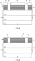
- a second sacrificial layer 27 ( Figure 8 ) is then formed on the insulating gate structure 17, on the source electrode 20 and on the drain electrode 22 and defined by a second photolithographic process.
- the second sacrificial layer 27 has an opening 28 for the formation of the gate electrode 18.
- the gate electrode 18 is formed in a position corresponding to the opening 28.
- a further annealing step may be performed after the deposition of the metal layer or multilayer, for example at 400 °C.
- the HEMT device 10 of Figure 3 is obtained.
- the diffusion of the aluminum oxide layers 17a and the hafnium oxide layers 17b during annealing allows a high permittivity value, typically intermediate between the permittivity values of the single intrinsic Al 2 O 3 and HfO 2 layers, to be maintained, while avoiding crystallization of the material during subsequent high temperature processing steps.
- the resistance to high temperatures advantageously allows the gate stack 17' to be formed before forming the source and drain electrodes with the respective ohmic contacts without the material being degraded. In this manner a single photolithographic process and a single annealing step may be used to both define the insulating gate structure 17 and to form the source and drain electrodes with the respective ohmic contacts.
- the gate region here indicated by 38, may be of a recess type and insulating gate structure 40 is not planar.
- the barrier layer 16 is selectively plasma etched to open a trench 41 before forming the insulating multilayer 40', which is conformally deposited by ALD ( Figure 10 ).
- a vertical MOSFET 100 comprises a semiconductor structure 102 of silicon carbide (SiC), has a drain electrode 100a on a rear side 102a of the semiconductor structure 102 and source electrodes 100b and a gate electrode 100c on a front side 102b of the semiconductor structure 102.
- the semiconductor structure 102 in turn comprises a substrate 103 (one face whereof defines the rear side 100a) and an epitaxial layer 105 (one face whereof defines the front side 102b of the semiconductor structure 102) both having conductivities of a first type, for example of N-type.
- the N-type substrate 103 of SiC has a first doping level that is higher (e.g. 10 18 atoms/cm 3 or greater), while the epitaxial layer 103 has a second doping level that is lower (e.g. 10 15 -10 16 atoms/cm 3 ).
- Body wells 107 having conductivity of a second type, here P-type, are formed inside the epitaxial layer 105 and accommodate respective source regions 108, with conductivity of the first type, in particular N+, and contact regions 109, with conductivity of the second type, in particular P+, and contiguous to respective source regions 108.
- the epitaxial layer 105 defines a Current Spread Layer (CSL) wherein the body wells 107 are embedded.
- CSL Current Spread Layer
- the body wells 107 are separated from each other by a distance normally less than 1 ⁇ m, for example 0.6 ⁇ m.
- the body wells 107 and the portion of the epitaxial layer 105 comprised therebetween form a parasitic JFET region.
- An insulating gate structure 110 extends on the front side 102a of the semiconductor structure 102 on the epitaxial layer 105 (or on the enhancement layer 6, if any) between the source regions 108 and is surmounted by the gate electrode 100b.
- the insulating gate structure 110 provided as already illustrated with reference to Figures 2a-2c , contains a mixture of aluminum, hafnium and oxygen. More precisely, the insulating gate structure 110 is obtained by the conformal deposition in alternated succession of a plurality of aluminum oxide layers and a plurality of hafnium oxide layers having nanometer or sub-nanometer thickness, followed by an annealing step.
- a semiconductor wafer 130 comprises the substrate 103, whereon the epitaxial layer 105 is grown to form the semiconductor structure 102.
- the body wells 107, the source regions 108 and the contact regions 109 are then formed by subsequent ion implantations of different doping species.
- an activation annealing step is carried out at a high temperature, for example above 1600 °C.
- a gate stack 110' is formed, as described with reference to Figure 2a .
- the gate stack 110' is obtained by the conformal deposition in alternated succession of a plurality of aluminum oxide layers 110a and a plurality of hafnium oxide layers 110b having nanometer thickness, until they reach an overall desired thickness.
- the aluminum oxide layers 110a and the hafnium oxide layers 17b are formed by Atomic Layer Deposition (ALD).
- a first sacrificial layer 112 of resist is formed on the gate stack 110' and defined by a first photolithographic process.
- the first sacrificial layer 112 has openings 113 for the formation of the source electrodes 100b and is used as a mask to selectively etch the gate stack 110'.
- the source electrodes 100b are formed in positions corresponding to respective openings 113.
- a metal layer or multilayer is also deposited on the rear side 102a of the semiconductor structure 102e to form the drain electrode 100a.
- the substrate 103 may be mechanically thinned (grinded) and possibly be subject to laser annealing.
- an annealing step is carried out, for example at an annealing temperature of 800 °C for the formation of silicides.
- the gate stack 110' is heated to the annealing temperature, the aluminum oxide and hafnium oxide of the layers 110a, 110b of the gate stack 110' diffuse at the interfaces and mix.
- the mixture of aluminum, hafnium and oxygen is present.
- the starting layered structure may be partially preserved (as in the example of Figure 2b ) or, alternatively, may be lost (as in the example of Figure 2c ).
- a metal layer or multilayer 115 of a material different from the material used for the source electrodes 100b, is deposited on the insulating gate structure 110 and on the source electrodes 100b, then a second sacrificial layer 120 of resist is formed on part of the metal layer or multilayer 115 and is defined by a second photolithographic process.
- the second sacrificial layer 120 has openings 121 for the formation of the gate electrodes 100c.
- the second sacrificial layer 120 is used as a mask to selectively etch the metal layer or multilayer 115 through the openings 121, for example by plasma etching.
- the gate electrode 100c is thus obtained.
- the MOSFET 100 of Figure 11 is obtained.
- the insulating gate structure 117 and the manufacturing process described allow high-permittivity dielectrics to be used as gate insulators in SiC MOSFETs instead of silicon oxide, for example, with a double advantage.
- the high permittivity allows the highest electric field values to be localized within the epitaxial layer 105. It is thus possible to optimize both the thickness of the same epitaxial layer 105 and the on-state resistance RON.
- the process flow is simplified because the nitric oxide post-oxidation annealing steps at high temperature (1100 - 1200 °C) are eliminated.
Landscapes
- Insulated Gate Type Field-Effect Transistor (AREA)
- Thin Film Transistor (AREA)
- Junction Field-Effect Transistors (AREA)
- Engineering & Computer Science (AREA)
- Manufacturing & Machinery (AREA)
Applications Claiming Priority (1)
| Application Number | Priority Date | Filing Date | Title |
|---|---|---|---|
| IT102022000001478A IT202200001478A1 (it) | 2022-01-28 | 2022-01-28 | Transistore ad ampia banda proibita con struttura isolante di porta nanolaminata e procedimento per fabbricare un transistore ad ampia banda proibita |
Publications (3)
| Publication Number | Publication Date |
|---|---|
| EP4220734A1 EP4220734A1 (en) | 2023-08-02 |
| EP4220734B1 true EP4220734B1 (en) | 2024-11-20 |
| EP4220734C0 EP4220734C0 (en) | 2024-11-20 |
Family
ID=80933659
Family Applications (1)
| Application Number | Title | Priority Date | Filing Date |
|---|---|---|---|
| EP23152421.6A Active EP4220734B1 (en) | 2022-01-28 | 2023-01-19 | Wide band gap transistor with nanolaminated insulating gate strutcture and process for manufacturing a wide band gap transistor |
Country Status (4)
| Country | Link |
|---|---|
| US (1) | US20230246086A1 (https=) |
| EP (1) | EP4220734B1 (https=) |
| JP (1) | JP2023110900A (https=) |
| IT (1) | IT202200001478A1 (https=) |
Families Citing this family (2)
| Publication number | Priority date | Publication date | Assignee | Title |
|---|---|---|---|---|
| CN117995661B (zh) * | 2024-01-23 | 2025-02-07 | 安徽大学 | 基于SiC衬底的开关器件栅氧层的制备方法及开关器件 |
| WO2026009769A1 (ja) * | 2024-07-04 | 2026-01-08 | 東京エレクトロン株式会社 | 成膜方法、成膜装置及び半導体デバイス |
-
2022
- 2022-01-28 IT IT102022000001478A patent/IT202200001478A1/it unknown
-
2023
- 2023-01-18 US US18/156,120 patent/US20230246086A1/en active Pending
- 2023-01-19 EP EP23152421.6A patent/EP4220734B1/en active Active
- 2023-01-26 JP JP2023010393A patent/JP2023110900A/ja active Pending
Also Published As
| Publication number | Publication date |
|---|---|
| EP4220734A1 (en) | 2023-08-02 |
| US20230246086A1 (en) | 2023-08-03 |
| JP2023110900A (ja) | 2023-08-09 |
| EP4220734C0 (en) | 2024-11-20 |
| IT202200001478A1 (it) | 2023-07-28 |
Similar Documents
| Publication | Publication Date | Title |
|---|---|---|
| US8354715B2 (en) | Semiconductor device and method of fabricating the same | |
| US9837519B2 (en) | Semiconductor device | |
| JP3216804B2 (ja) | 炭化けい素縦形fetの製造方法および炭化けい素縦形fet | |
| US8525274B2 (en) | Semiconductor device and method of manufacturing the same | |
| JP7804606B2 (ja) | 半導体装置及びその製造方法 | |
| US20140209999A1 (en) | Semiconductor device | |
| US11670502B2 (en) | SiC MOSFET and method for manufacturing the same | |
| US8941120B2 (en) | Semiconductor device and method for manufacturing the same | |
| CN104638010B (zh) | 一种横向导通的GaN常关型MISFET器件及其制作方法 | |
| EP4220734B1 (en) | Wide band gap transistor with nanolaminated insulating gate strutcture and process for manufacturing a wide band gap transistor | |
| JP7588660B2 (ja) | 段階的な横方向ドーピングを有する半導体パワーデバイスおよびそのようなデバイスを形成する方法 | |
| JP2019186458A (ja) | スイッチング素子とその製造方法 | |
| JP6584671B2 (ja) | 半導体装置およびその製造方法 | |
| JP2016521460A (ja) | ヘテロ接合トランジスタに通常は妨げられる注入領域を形成する方法 | |
| US20200287045A1 (en) | Semiconductor device and method for producing the same | |
| JP2010027833A (ja) | 炭化珪素半導体装置およびその製造方法 | |
| JP5526493B2 (ja) | トレンチゲート型半導体装置およびその製造方法 | |
| US20250203977A1 (en) | Silicon carbide vertical conduction mosfet device for power applications and manufacturing process thereof | |
| US12255233B2 (en) | Silicon carbide vertical conduction MOSFET device for power applications and manufacturing process thereof | |
| JP7513565B2 (ja) | スイッチング素子の製造方法 | |
| CN116525669A (zh) | 具有纳米叠层绝缘栅极结构的宽带隙晶体管和制造工艺 | |
| US20250357122A1 (en) | Method of manufacturing a semiconductor device including an ohmic contact and a gate dielectric | |
| US20240079237A1 (en) | Method of manufacturing ohmic contacts of an electronic device, with thermal budget optimization | |
| US20250203954A1 (en) | Power semiconductor devices | |
| US11881526B2 (en) | Semiconductor device and method for manufacturing same |
Legal Events
| Date | Code | Title | Description |
|---|---|---|---|
| PUAI | Public reference made under article 153(3) epc to a published international application that has entered the european phase |
Free format text: ORIGINAL CODE: 0009012 |
|
| STAA | Information on the status of an ep patent application or granted ep patent |
Free format text: STATUS: THE APPLICATION HAS BEEN PUBLISHED |
|
| AK | Designated contracting states |
Kind code of ref document: A1 Designated state(s): AL AT BE BG CH CY CZ DE DK EE ES FI FR GB GR HR HU IE IS IT LI LT LU LV MC ME MK MT NL NO PL PT RO RS SE SI SK SM TR |
|
| STAA | Information on the status of an ep patent application or granted ep patent |
Free format text: STATUS: REQUEST FOR EXAMINATION WAS MADE |
|
| 17P | Request for examination filed |
Effective date: 20231228 |
|
| RBV | Designated contracting states (corrected) |
Designated state(s): AL AT BE BG CH CY CZ DE DK EE ES FI FR GB GR HR HU IE IS IT LI LT LU LV MC ME MK MT NL NO PL PT RO RS SE SI SK SM TR |
|
| GRAP | Despatch of communication of intention to grant a patent |
Free format text: ORIGINAL CODE: EPIDOSNIGR1 |
|
| STAA | Information on the status of an ep patent application or granted ep patent |
Free format text: STATUS: GRANT OF PATENT IS INTENDED |
|
| RIC1 | Information provided on ipc code assigned before grant |
Ipc: H01L 29/78 20060101ALI20240606BHEP Ipc: H01L 29/778 20060101ALI20240606BHEP Ipc: H01L 29/20 20060101ALI20240606BHEP Ipc: H01L 21/28 20060101ALI20240606BHEP Ipc: H01L 21/04 20060101ALI20240606BHEP Ipc: H01L 29/16 20060101ALI20240606BHEP Ipc: H01L 29/51 20060101AFI20240606BHEP |
|
| INTG | Intention to grant announced |
Effective date: 20240621 |
|
| RIN1 | Information on inventor provided before grant (corrected) |
Inventor name: ROCCAFORTE, FABRIZIO Inventor name: SCHILIRO', EMANUELA Inventor name: LO NIGRO, RAFFAELLA Inventor name: IUCOLANO, FERDINANDO |
|
| GRAS | Grant fee paid |
Free format text: ORIGINAL CODE: EPIDOSNIGR3 |
|
| GRAA | (expected) grant |
Free format text: ORIGINAL CODE: 0009210 |
|
| STAA | Information on the status of an ep patent application or granted ep patent |
Free format text: STATUS: THE PATENT HAS BEEN GRANTED |
|
| AK | Designated contracting states |
Kind code of ref document: B1 Designated state(s): AL AT BE BG CH CY CZ DE DK EE ES FI FR GB GR HR HU IE IS IT LI LT LU LV MC ME MK MT NL NO PL PT RO RS SE SI SK SM TR |
|
| REG | Reference to a national code |
Ref country code: GB Ref legal event code: FG4D |
|
| REG | Reference to a national code |
Ref country code: DE Ref legal event code: R079 Ref document number: 602023001028 Country of ref document: DE Free format text: PREVIOUS MAIN CLASS: H01L0029510000 Ipc: H10D0064680000 |
|
| REG | Reference to a national code |
Ref country code: CH Ref legal event code: EP |
|
| REG | Reference to a national code |
Ref country code: DE Ref legal event code: R096 Ref document number: 602023001028 Country of ref document: DE |
|
| REG | Reference to a national code |
Ref country code: IE Ref legal event code: FG4D |
|
| U01 | Request for unitary effect filed |
Effective date: 20241121 |
|
| U07 | Unitary effect registered |
Designated state(s): AT BE BG DE DK EE FI FR IT LT LU LV MT NL PT RO SE SI Effective date: 20241128 |
|
| U20 | Renewal fee for the european patent with unitary effect paid |
Year of fee payment: 3 Effective date: 20241218 |
|
| PG25 | Lapsed in a contracting state [announced via postgrant information from national office to epo] |
Ref country code: IS Free format text: LAPSE BECAUSE OF FAILURE TO SUBMIT A TRANSLATION OF THE DESCRIPTION OR TO PAY THE FEE WITHIN THE PRESCRIBED TIME-LIMIT Effective date: 20250320 Ref country code: HR Free format text: LAPSE BECAUSE OF FAILURE TO SUBMIT A TRANSLATION OF THE DESCRIPTION OR TO PAY THE FEE WITHIN THE PRESCRIBED TIME-LIMIT Effective date: 20241120 |
|
| PG25 | Lapsed in a contracting state [announced via postgrant information from national office to epo] |
Ref country code: ES Free format text: LAPSE BECAUSE OF FAILURE TO SUBMIT A TRANSLATION OF THE DESCRIPTION OR TO PAY THE FEE WITHIN THE PRESCRIBED TIME-LIMIT Effective date: 20241120 |
|
| PG25 | Lapsed in a contracting state [announced via postgrant information from national office to epo] |
Ref country code: NO Free format text: LAPSE BECAUSE OF FAILURE TO SUBMIT A TRANSLATION OF THE DESCRIPTION OR TO PAY THE FEE WITHIN THE PRESCRIBED TIME-LIMIT Effective date: 20250220 |
|
| PG25 | Lapsed in a contracting state [announced via postgrant information from national office to epo] |
Ref country code: GR Free format text: LAPSE BECAUSE OF FAILURE TO SUBMIT A TRANSLATION OF THE DESCRIPTION OR TO PAY THE FEE WITHIN THE PRESCRIBED TIME-LIMIT Effective date: 20250221 |
|
| PG25 | Lapsed in a contracting state [announced via postgrant information from national office to epo] |
Ref country code: PL Free format text: LAPSE BECAUSE OF FAILURE TO SUBMIT A TRANSLATION OF THE DESCRIPTION OR TO PAY THE FEE WITHIN THE PRESCRIBED TIME-LIMIT Effective date: 20241120 |
|
| PG25 | Lapsed in a contracting state [announced via postgrant information from national office to epo] |
Ref country code: RS Free format text: LAPSE BECAUSE OF FAILURE TO SUBMIT A TRANSLATION OF THE DESCRIPTION OR TO PAY THE FEE WITHIN THE PRESCRIBED TIME-LIMIT Effective date: 20250220 |
|
| PG25 | Lapsed in a contracting state [announced via postgrant information from national office to epo] |
Ref country code: SM Free format text: LAPSE BECAUSE OF FAILURE TO SUBMIT A TRANSLATION OF THE DESCRIPTION OR TO PAY THE FEE WITHIN THE PRESCRIBED TIME-LIMIT Effective date: 20241120 |
|
| PG25 | Lapsed in a contracting state [announced via postgrant information from national office to epo] |
Ref country code: SK Free format text: LAPSE BECAUSE OF FAILURE TO SUBMIT A TRANSLATION OF THE DESCRIPTION OR TO PAY THE FEE WITHIN THE PRESCRIBED TIME-LIMIT Effective date: 20241120 |
|
| PG25 | Lapsed in a contracting state [announced via postgrant information from national office to epo] |
Ref country code: CZ Free format text: LAPSE BECAUSE OF FAILURE TO SUBMIT A TRANSLATION OF THE DESCRIPTION OR TO PAY THE FEE WITHIN THE PRESCRIBED TIME-LIMIT Effective date: 20241120 |
|
| PG25 | Lapsed in a contracting state [announced via postgrant information from national office to epo] |
Ref country code: MC Free format text: LAPSE BECAUSE OF FAILURE TO SUBMIT A TRANSLATION OF THE DESCRIPTION OR TO PAY THE FEE WITHIN THE PRESCRIBED TIME-LIMIT Effective date: 20241120 |
|
| PLBE | No opposition filed within time limit |
Free format text: ORIGINAL CODE: 0009261 |
|
| STAA | Information on the status of an ep patent application or granted ep patent |
Free format text: STATUS: NO OPPOSITION FILED WITHIN TIME LIMIT |
|
| 26N | No opposition filed |
Effective date: 20250821 |
|
| PG25 | Lapsed in a contracting state [announced via postgrant information from national office to epo] |
Ref country code: IE Free format text: LAPSE BECAUSE OF NON-PAYMENT OF DUE FEES Effective date: 20250119 |
|
| U20 | Renewal fee for the european patent with unitary effect paid |
Year of fee payment: 4 Effective date: 20251217 |