EP4207291A1 - Rückwandplatine und verfahren zur herstellung davon sowie hintergrundbeleuchtungsmodul und anzeigevorrichtung - Google Patents
Rückwandplatine und verfahren zur herstellung davon sowie hintergrundbeleuchtungsmodul und anzeigevorrichtung Download PDFInfo
- Publication number
- EP4207291A1 EP4207291A1 EP21946456.7A EP21946456A EP4207291A1 EP 4207291 A1 EP4207291 A1 EP 4207291A1 EP 21946456 A EP21946456 A EP 21946456A EP 4207291 A1 EP4207291 A1 EP 4207291A1
- Authority
- EP
- European Patent Office
- Prior art keywords
- orthographic projection
- substrate
- extending portion
- backplane
- linear extending
- Prior art date
- Legal status (The legal status is an assumption and is not a legal conclusion. Google has not performed a legal analysis and makes no representation as to the accuracy of the status listed.)
- Granted
Links
Images


Classifications
-
- H—ELECTRICITY
- H10—SEMICONDUCTOR DEVICES; ELECTRIC SOLID-STATE DEVICES NOT OTHERWISE PROVIDED FOR
- H10H—INORGANIC LIGHT-EMITTING SEMICONDUCTOR DEVICES HAVING POTENTIAL BARRIERS
- H10H29/00—Integrated devices, or assemblies of multiple devices, comprising at least one light-emitting semiconductor element covered by group H10H20/00
- H10H29/30—Active-matrix LED displays
- H10H29/39—Connection of the pixel electrodes to the driving transistors
-
- H—ELECTRICITY
- H10—SEMICONDUCTOR DEVICES; ELECTRIC SOLID-STATE DEVICES NOT OTHERWISE PROVIDED FOR
- H10W—GENERIC PACKAGES, INTERCONNECTIONS, CONNECTORS OR OTHER CONSTRUCTIONAL DETAILS OF DEVICES COVERED BY CLASS H10
- H10W90/00—Package configurations
-
- G—PHYSICS
- G02—OPTICS
- G02F—OPTICAL DEVICES OR ARRANGEMENTS FOR THE CONTROL OF LIGHT BY MODIFICATION OF THE OPTICAL PROPERTIES OF THE MEDIA OF THE ELEMENTS INVOLVED THEREIN; NON-LINEAR OPTICS; FREQUENCY-CHANGING OF LIGHT; OPTICAL LOGIC ELEMENTS; OPTICAL ANALOGUE/DIGITAL CONVERTERS
- G02F1/00—Devices or arrangements for the control of the intensity, colour, phase, polarisation or direction of light arriving from an independent light source, e.g. switching, gating or modulating; Non-linear optics
- G02F1/01—Devices or arrangements for the control of the intensity, colour, phase, polarisation or direction of light arriving from an independent light source, e.g. switching, gating or modulating; Non-linear optics for the control of the intensity, phase, polarisation or colour
- G02F1/13—Devices or arrangements for the control of the intensity, colour, phase, polarisation or direction of light arriving from an independent light source, e.g. switching, gating or modulating; Non-linear optics for the control of the intensity, phase, polarisation or colour based on liquid crystals, e.g. single liquid crystal display cells
- G02F1/133—Constructional arrangements; Operation of liquid crystal cells; Circuit arrangements
- G02F1/1333—Constructional arrangements; Manufacturing methods
- G02F1/1335—Structural association of cells with optical devices, e.g. polarisers or reflectors
- G02F1/1336—Illuminating devices
- G02F1/133602—Direct backlight
- G02F1/133603—Direct backlight with LEDs
-
- G—PHYSICS
- G02—OPTICS
- G02F—OPTICAL DEVICES OR ARRANGEMENTS FOR THE CONTROL OF LIGHT BY MODIFICATION OF THE OPTICAL PROPERTIES OF THE MEDIA OF THE ELEMENTS INVOLVED THEREIN; NON-LINEAR OPTICS; FREQUENCY-CHANGING OF LIGHT; OPTICAL LOGIC ELEMENTS; OPTICAL ANALOGUE/DIGITAL CONVERTERS
- G02F1/00—Devices or arrangements for the control of the intensity, colour, phase, polarisation or direction of light arriving from an independent light source, e.g. switching, gating or modulating; Non-linear optics
- G02F1/01—Devices or arrangements for the control of the intensity, colour, phase, polarisation or direction of light arriving from an independent light source, e.g. switching, gating or modulating; Non-linear optics for the control of the intensity, phase, polarisation or colour
- G02F1/13—Devices or arrangements for the control of the intensity, colour, phase, polarisation or direction of light arriving from an independent light source, e.g. switching, gating or modulating; Non-linear optics for the control of the intensity, phase, polarisation or colour based on liquid crystals, e.g. single liquid crystal display cells
- G02F1/133—Constructional arrangements; Operation of liquid crystal cells; Circuit arrangements
- G02F1/1333—Constructional arrangements; Manufacturing methods
- G02F1/1335—Structural association of cells with optical devices, e.g. polarisers or reflectors
- G02F1/1336—Illuminating devices
- G02F1/133602—Direct backlight
- G02F1/133605—Direct backlight including specially adapted reflectors
-
- H—ELECTRICITY
- H10—SEMICONDUCTOR DEVICES; ELECTRIC SOLID-STATE DEVICES NOT OTHERWISE PROVIDED FOR
- H10H—INORGANIC LIGHT-EMITTING SEMICONDUCTOR DEVICES HAVING POTENTIAL BARRIERS
- H10H29/00—Integrated devices, or assemblies of multiple devices, comprising at least one light-emitting semiconductor element covered by group H10H20/00
- H10H29/01—Manufacture or treatment
- H10H29/036—Manufacture or treatment of packages
- H10H29/0362—Manufacture or treatment of packages of encapsulations
-
- H—ELECTRICITY
- H10—SEMICONDUCTOR DEVICES; ELECTRIC SOLID-STATE DEVICES NOT OTHERWISE PROVIDED FOR
- H10H—INORGANIC LIGHT-EMITTING SEMICONDUCTOR DEVICES HAVING POTENTIAL BARRIERS
- H10H29/00—Integrated devices, or assemblies of multiple devices, comprising at least one light-emitting semiconductor element covered by group H10H20/00
- H10H29/01—Manufacture or treatment
- H10H29/036—Manufacture or treatment of packages
- H10H29/0363—Manufacture or treatment of packages of optical field-shaping means
-
- H—ELECTRICITY
- H10—SEMICONDUCTOR DEVICES; ELECTRIC SOLID-STATE DEVICES NOT OTHERWISE PROVIDED FOR
- H10H—INORGANIC LIGHT-EMITTING SEMICONDUCTOR DEVICES HAVING POTENTIAL BARRIERS
- H10H29/00—Integrated devices, or assemblies of multiple devices, comprising at least one light-emitting semiconductor element covered by group H10H20/00
- H10H29/80—Constructional details
- H10H29/85—Packages
- H10H29/852—Encapsulations
- H10H29/853—Encapsulations characterised by their shape
-
- H—ELECTRICITY
- H10—SEMICONDUCTOR DEVICES; ELECTRIC SOLID-STATE DEVICES NOT OTHERWISE PROVIDED FOR
- H10H—INORGANIC LIGHT-EMITTING SEMICONDUCTOR DEVICES HAVING POTENTIAL BARRIERS
- H10H29/00—Integrated devices, or assemblies of multiple devices, comprising at least one light-emitting semiconductor element covered by group H10H20/00
- H10H29/80—Constructional details
- H10H29/85—Packages
- H10H29/855—Optical field-shaping means, e.g. lenses
- H10H29/856—Reflecting means
-
- H—ELECTRICITY
- H10—SEMICONDUCTOR DEVICES; ELECTRIC SOLID-STATE DEVICES NOT OTHERWISE PROVIDED FOR
- H10W—GENERIC PACKAGES, INTERCONNECTIONS, CONNECTORS OR OTHER CONSTRUCTIONAL DETAILS OF DEVICES COVERED BY CLASS H10
- H10W70/00—Package substrates; Interposers; Redistribution layers [RDL]
- H10W70/01—Manufacture or treatment
- H10W70/05—Manufacture or treatment of insulating or insulated package substrates, or of interposers, or of redistribution layers
-
- H—ELECTRICITY
- H10—SEMICONDUCTOR DEVICES; ELECTRIC SOLID-STATE DEVICES NOT OTHERWISE PROVIDED FOR
- H10W—GENERIC PACKAGES, INTERCONNECTIONS, CONNECTORS OR OTHER CONSTRUCTIONAL DETAILS OF DEVICES COVERED BY CLASS H10
- H10W70/00—Package substrates; Interposers; Redistribution layers [RDL]
- H10W70/60—Insulating or insulated package substrates; Interposers; Redistribution layers
- H10W70/611—Insulating or insulated package substrates; Interposers; Redistribution layers for connecting multiple chips together
-
- H—ELECTRICITY
- H10—SEMICONDUCTOR DEVICES; ELECTRIC SOLID-STATE DEVICES NOT OTHERWISE PROVIDED FOR
- H10W—GENERIC PACKAGES, INTERCONNECTIONS, CONNECTORS OR OTHER CONSTRUCTIONAL DETAILS OF DEVICES COVERED BY CLASS H10
- H10W70/00—Package substrates; Interposers; Redistribution layers [RDL]
- H10W70/60—Insulating or insulated package substrates; Interposers; Redistribution layers
- H10W70/62—Insulating or insulated package substrates; Interposers; Redistribution layers characterised by their interconnections
- H10W70/65—Shapes or dispositions of interconnections
Definitions
- the present disclosure relates to the field of display technologies, and in particular, to a backplane and a method for manufacturing the same, and a backlight module and display apparatuses.
- a backplane in an aspect, includes a substrate, a circuit structure layer located on a side of the substrate, a reflective layer located on a side of the circuit structure layer away from the substrate, a plurality of electronic devices and a plurality of encapsulation portions.
- the reflective layer includes a plurality of first through holes arranged at intervals. Each electronic device is located in a first through hole, and the plurality of electronic devices are electrically connected to the circuit structure layer.
- Each encapsulation portion covers an electronic device.
- a conductive layer in the circuit structure layer farthest from the substrate includes a plurality of first conductive lines, and at least one first conductive line includes a first linear extending portion, a second linear extending portion and a third linear extending portion.
- An orthographic projection of the first linear extending portion on the substrate is a first orthographic projection
- an orthographic projection of the second linear extending portion on the substrate is a second orthographic projection
- an orthographic projection of the third linear extending portion on the substrate is a third orthographic projection
- an orthographic projection of an encapsulation portion on the substrate is a fourth orthographic projection.
- the first orthographic projection is located within the fourth orthographic projection
- the second orthographic projection is partially overlapped with the fourth orthographic projection
- the third orthographic projection is located outside the fourth orthographic projection.
- Two endpoints of the fourth orthographic projection that are farthest from each other in a width direction of the second linear extending portion are first endpoints.
- a distance between the second orthographic projection and each of first reference lines, which respectively pass through the first endpoints and are parallel to the second linear extending portion is not less than half of a line width of the second linear extending portion.
- the distance between the second orthographic projection and each of the first reference lines, which respectively pass through the first endpoints and are parallel to the second linear extending portion is greater than or equal to 0.15 mm.
- the distance between the first orthographic projection and each of the second reference lines, which respectively pass through the second endpoints and are parallel to the first linear extending portion is greater than or equal to 0.15 mm.
- the at least one first conductive line further includes a first connection portion connecting the first linear extending portion and the second linear extending portion, and a second connection portion connecting the second linear extending portion and the third linear extending portion.
- An orthographic projection of the first connection portion on the substrate is located within the fourth orthographic projection, and an orthographic projection of the second connection portion on the substrate is located outside the fourth orthographic projection.
- an extending direction of the first linear extending portion is perpendicular to an extending direction of the second linear extending portion; and/or the extending direction of the second linear extending portion is perpendicular to an extending direction of the third linear extending portion.
- a distance between the orthographic projection of the first connection portion on the substrate and the fourth orthographic projection is greater than or equal to 0.25 mm; and/or a distance between the orthographic projection of the second connection portion on the substrate and the fourth orthographic projection is greater than or equal to 0.25 mm.
- a shape of the fourth orthographic projection is a circle or substantially a circle.
- a radius of the circle is greater than or equal to 1.25 mm, or is less than or equal to 1.0 mm.
- the plurality of electronic devices include at least one light-emitting device and at least one driver chip.
- the circuit structure layer includes two conductive layers.
- a conductive layer in the two conductive layers farther from the substrate is a first conductive layer
- a conductive layer in the two conductive layers closer to the substrate is a second conductive layer.
- the second conductive layer includes a plurality of second conductive lines.
- the circuit structure layer further includes a first insulating layer located between the first conductive layer and the second conductive layer, and a first transition layer located between the second conductive layer and the first insulating layer.
- the backplane further includes a second transition layer, a second insulating layer and a third transition layer.
- the second transition layer is located between the substrate and the second conductive layer.
- the second insulating layer is located between the first conductive layer and the reflective layer.
- the third transition layer is located between the first conductive layer and the second insulating layer.
- a backlight module in another aspect, includes the backplane in any one of the above embodiments, and the plurality of electronic devices in the backplane include a plurality of light-emitting devices.
- the backlight module further includes a diffusion plate, a quantum dot film, a diffusion sheet, a composite film and a plurality of support pillars.
- the diffusion plate is located on a light-emitting side of the backplane.
- the quantum dot film is located on a side of the diffusion plate away from the backplane.
- the diffusion sheet is located on a side of the quantum dot film away from the diffusion plate.
- the composite film is located on a side of the diffusion sheet away from the quantum dot film.
- the plurality of support pillars are located between the backplane and the diffusion plate.
- a display apparatus in yet another aspect, includes the backlight module in any one of the above embodiments, and a liquid crystal display panel located on a light exit side of the backlight module.
- a conductive layer in the circuit structure layer farthest from the substrate includes a plurality of first conductive lines, and at least one first conductive line includes a first linear extending portion, a second linear extending portion and a third linear extending portion.
- An orthographic projection of the first linear extending portion on the substrate is a first orthographic projection
- an orthographic projection of the second linear extending portion on the substrate is a second orthographic projection
- an orthographic projection of the third linear extending portion on the substrate is a third orthographic projection
- an orthographic projection of an encapsulation portion on the substrate is a fourth orthographic projection.
- the first orthographic projection is located within the fourth orthographic projection, the second orthographic projection is partially overlapped with the fourth orthographic projection, and the third orthographic projection is located outside the fourth orthographic projection.
- Two endpoints of the fourth orthographic projection that are farthest from each other in a width direction of the second linear extending portion are first endpoints.
- a distance between the second orthographic projection and each of first reference lines, which respectively pass through the first endpoints and are parallel to the second linear extending portion, is not less than half of a line width of the second linear extending portion.
- the method for manufacturing the backplane further includes: forming a plurality of reflective portions on a side of the reflective layer away from the substrate. Each reflective portion covers an edge of the first through hole, and the reflective portion defines a second through hole in the first through hole. The electronic device is located in the second through hole.
- the method for manufacturing the backplane before forming the second conductive layer on the side of the substrate, further includes: forming a second transition layer on the side of the substrate. Before forming the reflective layer on the side of the circuit structure layer away from the substrate, the method for manufacturing the backplane further includes: forming a third transition layer on a side of the first conductive layer away from the first insulating layer; and forming a second insulating layer on a side of the third transition layer away from the first conductive layer.
- first and second are only used for descriptive purposes, and are not to be construed as indicating or implying relative importance or implicitly indicating the number of indicated technical features.
- a feature defined with “first” or “second” may explicitly or implicitly include one or more of the features.
- the term "a plurality of/the plurality of” means two or more unless otherwise specified.
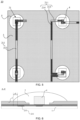
- a conductive layer 21 in the circuit structure layer 2 farthest from the substrate 1 includes a plurality of first conductive lines 211.
- At least one first conductive line 211 includes a first linear extending portion 212, a second linear extending portion 213 and a third linear extending portion 214.
- the reflective layer 3 is used for reflecting light incident on a surface of the reflective layer 3 away from the circuit structure layer 2, so as to improve a light utilization rate of the backplane 10.
- the reflective layer 3 may be made of white ink, and a reflectivity of the white ink to light is about 90 %. In this way, the reflective layer 3 is able to reflect more light, thereby achieving a better light utilization effect.
- the light-emitting device 41 may be a mini light-emitting diode.
- the driver chip 42 may be configured to control light-emitting state(s) of at least one light-emitting device 41, e.g., to control whether the at least one light-emitting device 41 emits light or not.
- a driver chip 42 may control light-emitting states of four light-emitting devices 41.
- a driver chip 42 may control light-emitting states of nine light-emitting devices 41.
- the number of light-emitting devices 41 controlled by a driver chip 42 is not limited in the present disclosure, as long as the backplane 10 is able to emit light normally.
- the plurality of first conductive lines 211 included in the conductive layer 21 in the circuit structure layer 2 farthest from the substrate 1 may not all include the first linear extending portion 212, the second linear extending portion 213 and the third linear extending portion 214.
- part of the plurality of first conductive lines 211 each may include only second linear extending portion(s) 213 and a third linear extending portion 214, and part of the plurality of first conductive lines 211 each may include only a second linear extending portion 213.
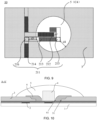
- the orthographic projection (i.e., the first orthographic projection C1) of the first linear extending portion 212 on the substrate 1 is located within the orthographic projection (i.e., the fourth orthographic projection C4) of the encapsulation portion 5 on the substrate 1, so that an orthographic projection of an edge of the encapsulation portion 5 on the substrate 1 may be non-overlapped with the orthographic projection of the first linear extending portion 212 on the substrate 1.
- the stress concentration region does not coincide with a region where the first linear extending portion 212 is located. That is, the stress concentration region is non-overlapped with a region having weak film adhesion.
- the distance d1 between the orthographic projection of the second linear extending portion 213 on the substrate 1 and each of the first reference lines M, which respectively pass through the first endpoints Q and are parallel to the second linear extending portion 213, is not less than half of the line width of the second linear extending portion 213. Therefore, the encapsulation portion 5 covers not only a region where the second linear extending portion 213 is located, but also regions respectively located on two sides of the second linear extending portion 213.
- regions respectively located on the two sides of the second linear extending portion 213 each have strong film adhesion
- the stress concentration region at the position corresponding to the edge of the encapsulation portion 5 in the backplane 10 is overlapped with the regions each having strong film adhesion, and the film adhesion is able to be offset with a shrinkage force of the encapsulation portion 5. Therefore, the risks of the peeling of the encapsulation portion 5, the chapping of the reflective layer, and breakage of the second linear extending portion 213 are effectively reduced, so that the problem that the electronic device 4 in the backplane 10 cannot operate normally due to the first conductive line 211 may be further solved. Therefore, the ability of the backplane 10 to resist the cold and hot shock is effectively improved, the use stability of the backplane 10 is enhanced, and the service life of the backplane 10 is prolonged.
- the orthographic projection (i.e., the third orthographic projection C3) of the third linear extending portion 214 on the substrate 1 is located outside the orthographic projection (i.e., the fourth orthographic projection C4) of the encapsulation portion 5 on the substrate 1, so that the orthographic projection of the edge of the encapsulation portion 5 on the substrate 1 is non-overlapped with the orthographic projection of the third linear extending portion 214 on the substrate 1.
- the stress concentration region does not coincide with a region where the third linear extending portion 214 is located. That is, the stress concentration region is non-overlapped with a region having weak film adhesion.
- the distance d1 between the second orthographic projection C2 and each of the first reference lines M, which respectively pass through the first endpoints Q and are parallel to the second linear extending portion 213, may be 0.15 mm, 0.16 mm, 0.17 mm, or 0.20 mm.
- the second orthographic projection C2 is far away from the first endpoints Q, so that the regions respectively located on the two sides of the second linear extending portion 213 each have a large area covered by the encapsulation portion 5. Therefore, the edge of the encapsulation portion 5 has a large region overlapped with the region having strong film adhesion in the backplane 10, and the region where the film adhesion is offset with the shrinkage force of the encapsulation portion 5 is large, so that the peeling of the encapsulation portion 5, the chapping of the reflective layer, and the breakage of the second linear extending portion 213 are less likely to occur in the backplane 10.
- the problem that the electronic device 4 in the backplane 10 cannot operate normally due to the breakage of the first conductive line is further solved, so that the ability of the backplane 10 to resist the cold and hot shock is effectively improved, the use stability of the backplane 10 is enhanced, and the service life of the backplane 10 is prolonged.
- two endpoints of the fourth orthographic projection C4 that are farthest from each other in a width direction of the first linear extending portion 212 are second endpoints W
- a distance d2 between the first orthographic projection C1 and each of second reference lines N, which respectively pass through the second endpoints W and are parallel to the first linear extending portion 212, is not less than half of a line width of the first linear extending portion 212.
- the distance d2 between the first orthographic projection C1 and each the second reference lines N, which respectively pass through the second endpoints W and are parallel to the first linear extending portion 212 may be 0.18 mm.
- regions respectively located on the two sides of the first linear extending portion 212 each have strong film adhesion
- the stress concentration region at the position corresponding to the edge of the encapsulation portion 5 in the backplane 10 is overlapped with the regions each having strong film adhesion, and the film adhesion is able to be offset with the shrinkage force of the encapsulation portion 5. Therefore, the risks of the peeling of the encapsulation portion 5, the chapping of the reflective layer, and the breakage of the first linear extending portion 212 are effectively reduced, so that the problem that the electronic device 4 in the backplane 10 cannot operate normally due to the first conductive line 211 may be further solved. Therefore, the ability of the backplane 10 to resist the cold and hot shock is effectively improved, the use stability of the backplane 10 is enhanced, and the service life of the backplane 10 is prolonged.
- the distance d2 between the first orthographic projection C1 and each of the second reference lines N, which respectively pass through the second endpoints W and are parallel to the first linear extending portion 212 may be 0.15 mm, 0.16 mm, 0.17 mm, or 0.20 mm.
- the first orthographic projection C1 is far away from the second endpoints W, so that the regions respectively located on the two sides of the first linear extending portion 212 each have a large area covered by the encapsulation portion 5. Therefore, the edge of the encapsulation portion 5 has a large region overlapped with the region having strong film adhesion in the backplane 10, and the region where the film adhesion is offset with the shrinkage force of the encapsulation portion 5 is large, so that the peeling of the encapsulation portion 5, the chapping of the reflective layer, and the breakage of the first linear extending portion 212 are less likely to occur in the backplane 10.
- the problem that the electronic device 4 in the backplane 10 cannot operate normally due to the breakage of the first conductive line is further solved, so that the ability of the backplane 10 to resist the cold and hot shock is effectively improved, the use stability of the backplane 10 is enhanced, and the service life of the backplane 10 is prolonged.
- a distance d3 between the third orthographic projection C3 and the fourth orthographic projection C4 is not less than half of a line width of the third linear extending portion 214.
- the distance d3 between the third orthographic projection C3 and the fourth orthographic projection C4 is not less than 0.15 mm.
- the distance d3 between the third orthographic projection C3 and the fourth orthographic projection C4 may be 0.15 mm, 0.16 mm, 0.17 mm, or 0.20 mm.
- the third linear extending portion 214 is far away from the edge of the encapsulation portion 5, and when the ambient temperature changes, the stress concentration region does not coincide with a region having weak film adhesion. Therefore, the peeling of the encapsulation portion 5, the chapping of the reflective layer 3, and the breakage of the third linear extending portion 214 caused by the force are further avoided, so that the problem that the electronic device 4 in the backplane 10 cannot operate normally due to the breakage of the first conductive line is solved. Therefore, the ability of the backplane 10 to resist the cold and hot shock is effectively improved, the use stability of the backplane 10 is enhanced, and the service life of the backplane 10 is prolonged.
- the at least one first conductive line 211 further includes a first connection portion 215 connecting the first linear extending portion 212 and the second linear extending portion 213, and a second connection portion 216 connecting the second linear extending portion 213 and the third linear extending portion 214.
- An orthographic projection of the first connection portion 215 on the substrate 1 is located within the fourth orthographic projection C4, and an orthographic projection of the second connection portion 216 on the substrate 1 is located outside the fourth orthographic projection C4.
- the stress concentration region at the position corresponding to the edge of the encapsulation portion 5 in the backplane 10 does not coincide with a region where the first connection portion 215 is located and a region where the second connection portion 216 is located. That is, the shrinkage force of the encapsulation portion 5 does not directly act on the region where the first connection portion 215 is loacted and the region where the second connection portion 216 is located.
- the peeling of the encapsulation portion and the chapping of the reflective layer due to a fact that the region where the first connection portion is located and the region where the second connection portion is located each have weak film adhesion are avoided, and thus the problem that the electronic device 4 in the backplane 10 cannot operate normally when the temperature changes is solved. Therefore, the ability of the backplane 10 to resist the cold and hot shock is effectively improved, the use stability of the backplane 10 is enhanced, and the service life of the backplane 10 is prolonged.
- an extending direction of the first linear extending portion 212 is perpendicular to an extending direction of the second linear extending portion 213.
- a distance d4 between the orthographic projection of the first connection portion 215 on the substrate 1 and the fourth orthographic projection C4 is greater than or equal to 0.25 mm.
- a distance d5 between the orthographic projection of the second connection portion 216 on the substrate 1 and the fourth orthographic projection C4 is greater than or equal to 0.25 mm.
- the distance d5 between the orthographic projection of the second connection portion 216 on the substrate 1 and the fourth orthographic projection C4 may be 0.25 mm, 0.27 mm, or 0.30 mm.
- the stress concentration region is far away from the region where the second connection portion 216 is located, so that the peeling of the encapsulation portion and the chapping of the reflective layer are less likely to occur in the region where the second connection portion 216 is located when the ambient temperature changes, and the problem that the electronic device 4 in the backplane 10 cannot operate normally when the temperature changes is further solved. Therefore, the ability of the backplane 10 to resist the cold and hot shock is effectively improved, the use stability of the backplane 10 is enhanced, and the service life of the backplane 10 is prolonged.
- the distance d4 between the orthographic projection of the first connection portion 215 on the substrate 1 and the fourth orthographic projection C4 may be 0.25 mm, 0.27 mm, or 0.30 mm.
- the distance d5 between the orthographic projection of the second connection portion 216 on the substrate 1 and the fourth orthographic projection C4 may be 0.25 mm, 0.27 mm, or 0.30 mm.
- the stress concentration region is far away from both the region where the first connection portion 215 is located and the region where the second connection portion 216 is located, so that when the ambient temperature changes, the peeling of the encapsulation portion and the chapping of the reflective layer are less likely to occur in the region where the first connection portion 215 is located and the region where the second connection portion 216 is located, and the problem that the electronic device 4 in the backplane 10 cannot operate normally when the temperature changes is further solved. Therefore, the ability of the backplane 10 to resist the cold and hot shock is effectively improved, the use stability of the backplane 10 is enhanced, and the service life of the backplane 10 is prolonged.
- a radius of the fourth orthographic projection C4 is a distance from a center of a circle corresponding to a curvilinear border to any point on a non-curvilinear border.
- the shape of the fourth orthographic projection C4 is a circle or substantially a circle, so that in a case where the electronic device 4 is a light-emitting device 41, the encapsulation portion 5 may not only prevent the water vapor from entering the light-emitting device 41 to protect the light-emitting device 41 from corrosion or collision, but also converge light emitted from the light-emitting device 41, so as to improve a light extraction efficiency of the backplane 10.
- the radius of the circle is greater than or equal to 1.25 mm, so that the fourth orthographic projection C4 has a large area, and the encapsulation portion 5 is easier to cover the regions respectively located on the two sides of the first linear extending portion 212 and the regions respectively located on the two sides of the second linear extending portion 213.
- the shrinkage force of the encapsulation portion 5 is more likely to be offset by the film adhesion in the regions respectively located on the two sides of the first linear extending portion 212 and the regions respectively located on the two sides of the second linear extending portion 213, so that the peeling of the encapsulation portion, the chapping of the reflective layer, and the breakage of the linear extending portion are less likely to occur in the backplane 10.
- the problem that the electronic device 4 in the backplane 10 cannot operate normally due to a temperature change is solved, so that the ability of the backplane 10 to resist the cold and hot shock is improved, the use stability of the backplane 10 is enhanced, and the service life of the backplane 10 is prolonged.
- the radius of the circle is less than or equal to 1.0 mm, so that the fourth orthographic projection C4 has a small area, and the edge of the encapsulation portion 5 is less likely to fall in the region where the third linear extending portion 214 is located.
- the shrinkage force of the encapsulation portion 5 does not directly act on a region having weak film adhesion, so that the peeling of the encapsulation portion, the chapping of the reflective layer, and the breakage of the first conductive line are less likely to occur in the backplane 10.
- the problem that the electronic device 4 in the backplane 10 cannot operate normally due to a temperature change is solved, so that the ability of the backplane 10 to resist the cold and hot shock is improved, the use stability of the backplane 10 is enhanced, and the service life of the backplane 10 is prolonged.
- the line width of the first linear extending portion 212 is less than or equal to 0.2 mm.
- the line width of the second linear extending portion 213 is less than or equal to 0.2 mm.
- the line width of the third linear extending portion 214 is less than or equal to 0.2 mm.
- the line width of the first linear extending portion 212 may be 0.2 mm, 0.18 mm, or 0.16 mm.
- the line width of the second linear extending portion 213 may be 0.2 mm, 0.18 mm, or 0.16 mm.
- the line width of the third linear extending portion 214 may be 0.2 mm, 0.18 mm, or 0.16 mm.
- the line widths of the first linear extending portion 212, the second linear extending portion 213 and the third linear extending portion 214 may be equal or unequal.
- a region corresponding to the first conductive line 211 in the backplane 10 has a small area, and the region having weak film adhesion in the backplane 10 has a small area, so that a probability that the stress concentration region is overlapped with the region having weak film adhesion is reduced.
- the peeling of the encapsulation portion, the chapping of the reflective layer, and the breakage of the first conductive line are less likely to occur in the backplane 10, so that the problem that the electronic device 4 in the backplane 10 cannot operate normally due to a temperature change is solved.
- the ability of the backplane 10 to resist the cold and hot shock is improved, the use stability of the backplane 10 is enhanced, and the service life of the backplane 10 is prolonged.
- the backplate 10 further includes a plurality of reflective portions 6.
- Each reflective portion 6 covers an edge of a first through hole 31, and the reflective portion 6 defines a second through hole 61 in the first through hole 31.
- the electronic device 4 is located in the second through hole 61. In this way, when light reaches a region between the electronic device 4 and the edge of the first through hole 31, the reflective portion 6 is able to reflect the light, thereby improving a light extraction rate of the backplane 10.
- the reflective portion 6 may be made of white silica gel.
- the circuit structure layer 2 includes two conductive layers 21.
- a conductive layer 21 in the two conductive layers 21 farther from the substrate 1 is a first conductive layer 21A
- a conductive layer 21 in the two conductive layers 21 closer to the substrate 1 is a second conductive layer 21B.
- the second conductive layer 21B includes a plurality of second conductive lines 217.
- the circuit structure layer 2 further includes a first insulating layer 22 located between the first conductive layer 21A and the second conductive layer 21B and a first transition layer 23 located between the second conductive layer 21B and the first insulating layer 22.
- the first conductive lines 211 are disposed in the first conductive layer 21A, and the second conductive lines 217 are disposed in the second conductive layer 21B, so that an arrangement of the first conductive lines 211 and an arrangement of the second conductive lines 217 are simple, thereby reducing a difficulty of wiring in the backplane 10, saving cost, and improving the manufacturing efficiency of the backplane 10.
- the second transition layer 7 and the third transition layer 9 each may be made of an inorganic insulating material, such as silicon nitride.
- the second insulating layer 8 may be made of an organic insulating material.
- the second transition layer 7 and the third transition layer 9 are disposed, so that the region corresponding to the first conductive line 211 in the backplane 10 is able to have enhanced film adhesion.
- some embodiments of the present disclosure further provide a backlight module 100, and the backlight module 100 includes the backplane 10 in any one of the above embodiments.
- the plurality of electronic devices in the backplane 10 include a plurality of light-emitting devices 41.
- the backlight module 100 further includes a diffusion plate 20, a quantum dot film 30, a diffusion sheet 40, a composite film 50, and a plurality of support pillars 60.
- the diffusion plate 20 is located on a light-emitting side of the backplane 10.
- the quantum dot film 30 is located on a side of the diffusion plate 20 away from the backplane 10.
- the diffusion sheet 40 is located on a side of the quantum dot film 30 away from the diffusion plate 20.
- the composite film 50 is located on a side of the diffusion sheet 40 away from the quantum dot film 30.
- the plurality of support pillars 60 are located between the backplane 10 and the diffuser plate 20.
- the diffusion plate 20 and the diffusion sheet 40 are used for reducing light shadows generated by the backplane 10, so as to improve a light-emitting effect of the backlight module 100.
- the quantum dot film 30 may convert blue light into white light due to an excitation of the blue light emitted from the backplane 10, so as to improve a utilization rate of light.
- the composite film 50 may be used for increasing a brightness of the light emitted from the backplane 10.
- the support pillars 60 are used for supporting a plurality of films such as the diffusion plate 20, the quantum dot film 30, the diffusion sheet 40 and the composite film 50, so as to obtain a certain light-mixing distance and eliminate the light shadows.
- the light-mixing distance may be in a range of 1 mm to 10 mm, inclusive.
- the support pillar 60 may be made of polycarbonate (PC).
- the display apparatus 200 includes the backlight module 100 in any one of the above embodiments and a liquid crystal display panel 300 located on a light exit side of the backlight module 100.
- the display apparatus 200 may be any component with a display function, such as a television, a digital camera, a mobile phone, a watch, a tablet computer, a notebook computer, or a navigator.
- a display function such as a television, a digital camera, a mobile phone, a watch, a tablet computer, a notebook computer, or a navigator.
- Beneficial effects that may be achieved by the display apparatus 200 in some embodiments of the present disclosure are the same as the beneficial effects that may be achieved by the backlight module 100 in some embodiments of the present disclosure, and will not be repeated here.
- a reflective layer 3 is formed on a side of the circuit structure layer 2 away from the substrate 1.
- the reflective layer 3 includes a plurality of first through holes 31 arranged at intervals.
- a plurality of electronic devices 4 are mounted in the plurality of first through holes 31, respectively. Each electronic device 4 is located in a first through hole 31, and the plurality of electronic devices 4 are all electrically connected to the circuit structure layer 2.
- a plurality of encapsulation portions 5 are formed on a side of the plurality of electronic devices 4 away from the substrate 1. Each encapsulation portion 5 covers an electronic device 4.
- a conductive layer 21 in the circuit structure layer 2 farthest from the substrate 1 includes a plurality of first conductive lines 211.
- At least one first conductive line 211 includes a first linear extending portion 212, a second linear extending portion 213 and a third linear extending portion 214.
- An orthographic projection of the first linear extending portion 212 on the substrate 1 is a first orthographic projection C1
- an orthographic projection of the second linear extending portion 213 on the substrate 1 is a second orthographic projection C2
- an orthographic projection of the third linear extending portion 214 on the substrate 1 is a third orthographic projection C3
- an orthographic projection of the encapsulation portion 5 on the substrate 1 is a fourth orthographic projection C4.
- the first orthographic projection C1 is located within the fourth orthographic projection C4, the second orthographic projection C2 is partially overlapped with the fourth orthographic projection C4, and the third orthographic projection C3 is located outside the fourth orthographic projection C4.
- Two endpoints of the fourth orthographic projection C4 that are farthest from each other in a width direction of the second linear extending portion 213 are first endpoints Q.
- a distance d1 between the second orthographic projection C2 and each of first reference lines M, which respetively pass through the first endpoints Q and are parallel to the second linear extending portion 213, is not less than half of a line width of the second linear extending portion 213.
- the encapsulation portion 5 covers not only a region where the second linear extending portion 213 is located, but also regions respectively located on two sides of the second linear extending portion 213, when the ambient temperature changes, a stress concentration region occuring at a position corresponding to the edge of the encapsulation portion 5 in the backplane 10 is overlapped with a region having strong film adhesion, and the film adhesion is able to be offset with a shrinkage force of the encapsulation portion 5.
- the risks of the peeling of the encapsulation portion 5, the chapping of the reflective layer, and breakage of the second linear extending portion 213 are effectively reduced, so that the problem that the electronic device 4 in the backplane 10 cannot operate normally due to the first conductive line 211 may be further solved. Therefore, the ability of the backplane 10 to resist the cold and hot shock is effectively improved, the use stability of the backplane 10 is enhanced, and the service life of the backplane 10 is prolonged.
- a plurality of reflective portions 6 are formed on a side of the reflective layer 3 away from the substrate 1.
- Each reflective portion 6 covers an edge of a first through hole 31, and the reflective portion 6 defines a second through hole 61 in the first through hole 31.
- the electronic device 4 is located in the second through hole 61.
- forming the circuit structure layer 2 on the side of the substrate 1 includes S21 to S24.
- a second conductive layer 21B is formed on the side of the substrate 1.
- the second conductive layer 21B includes a plurality of second conductive lines 217.
- a first transition layer 23 is formed on a side of the second conductive layer 21B away from the substrate 1.
- a first conductive layer 21A is formed on a side of the first insulating layer 22 away from the first transition layer 23.
- a second transition layer 7 is formed on the side of the substrate 1.
- the method for manufacturing the backplane further includes S25 and S26.
- a second insulating layer 8 is formed on a side of the third transition layer 9 away from the first conductive layer 21A.
Landscapes
- Physics & Mathematics (AREA)
- Nonlinear Science (AREA)
- Mathematical Physics (AREA)
- Chemical & Material Sciences (AREA)
- Crystallography & Structural Chemistry (AREA)
- General Physics & Mathematics (AREA)
- Optics & Photonics (AREA)
- Devices For Indicating Variable Information By Combining Individual Elements (AREA)
- Geometry (AREA)
- Engineering & Computer Science (AREA)
- Ceramic Engineering (AREA)
- Planar Illumination Modules (AREA)
Priority Applications (1)
| Application Number | Priority Date | Filing Date | Title |
|---|---|---|---|
| EP25196079.5A EP4629792A3 (de) | 2021-06-24 | 2021-06-24 | Rückwandplatine und verfahren zur herstellung davon sowie hintergrundbeleuchtungsmodul und anzeigevorrichtung |
Applications Claiming Priority (1)
| Application Number | Priority Date | Filing Date | Title |
|---|---|---|---|
| PCT/CN2021/102192 WO2022266960A1 (zh) | 2021-06-24 | 2021-06-24 | 背板及其制作方法、背光模组、显示装置 |
Related Child Applications (2)
| Application Number | Title | Priority Date | Filing Date |
|---|---|---|---|
| EP25196079.5A Division-Into EP4629792A3 (de) | 2021-06-24 | 2021-06-24 | Rückwandplatine und verfahren zur herstellung davon sowie hintergrundbeleuchtungsmodul und anzeigevorrichtung |
| EP25196079.5A Division EP4629792A3 (de) | 2021-06-24 | 2021-06-24 | Rückwandplatine und verfahren zur herstellung davon sowie hintergrundbeleuchtungsmodul und anzeigevorrichtung |
Publications (3)
| Publication Number | Publication Date |
|---|---|
| EP4207291A1 true EP4207291A1 (de) | 2023-07-05 |
| EP4207291A4 EP4207291A4 (de) | 2024-01-03 |
| EP4207291B1 EP4207291B1 (de) | 2025-10-15 |
Family
ID=84543995
Family Applications (2)
| Application Number | Title | Priority Date | Filing Date |
|---|---|---|---|
| EP21946456.7A Active EP4207291B1 (de) | 2021-06-24 | 2021-06-24 | Rückwandplatine und verfahren zur herstellung davon sowie hintergrundbeleuchtungsmodul und anzeigevorrichtung |
| EP25196079.5A Pending EP4629792A3 (de) | 2021-06-24 | 2021-06-24 | Rückwandplatine und verfahren zur herstellung davon sowie hintergrundbeleuchtungsmodul und anzeigevorrichtung |
Family Applications After (1)
| Application Number | Title | Priority Date | Filing Date |
|---|---|---|---|
| EP25196079.5A Pending EP4629792A3 (de) | 2021-06-24 | 2021-06-24 | Rückwandplatine und verfahren zur herstellung davon sowie hintergrundbeleuchtungsmodul und anzeigevorrichtung |
Country Status (4)
| Country | Link |
|---|---|
| US (2) | US12176333B2 (de) |
| EP (2) | EP4207291B1 (de) |
| CN (1) | CN115720685A (de) |
| WO (1) | WO2022266960A1 (de) |
Cited By (2)
| Publication number | Priority date | Publication date | Assignee | Title |
|---|---|---|---|---|
| EP4300581A4 (de) * | 2021-07-30 | 2024-10-16 | BOE Technology Group Co., Ltd. | Arraysubstrat, herstellungsverfahren dafür, lichtemittierende vorrichtung und gekachelte anzeigevorrichtung |
| US12422712B2 (en) | 2022-05-31 | 2025-09-23 | Hefei BOE Ruisheng Technology Co., Ltd. | Light-emitting substrate and method of manufacturing the same, backlight module and display apparatus |
Families Citing this family (4)
| Publication number | Priority date | Publication date | Assignee | Title |
|---|---|---|---|---|
| US12306495B2 (en) * | 2022-08-26 | 2025-05-20 | Hefei BOE Ruisheng Technology Co., Ltd. | Substrate, backlight module and display device |
| CN117492259A (zh) * | 2023-02-06 | 2024-02-02 | Tcl华星光电技术有限公司 | 驱动背板及其制作方法、显示装置 |
| CN119072787A (zh) * | 2023-03-30 | 2024-12-03 | 京东方科技集团股份有限公司 | 发光基板及其制备方法、背光模组、显示装置 |
| CN117055265A (zh) * | 2023-09-15 | 2023-11-14 | 合肥京东方瑞晟科技有限公司 | 背光模组及其制备方法、显示装置 |
Family Cites Families (26)
| Publication number | Priority date | Publication date | Assignee | Title |
|---|---|---|---|---|
| JP4316019B2 (ja) | 1996-10-01 | 2009-08-19 | 株式会社東芝 | 半導体装置及び半導体装置製造方法 |
| JP4754850B2 (ja) | 2004-03-26 | 2011-08-24 | パナソニック株式会社 | Led実装用モジュールの製造方法及びledモジュールの製造方法 |
| JP5046521B2 (ja) | 2006-01-18 | 2012-10-10 | 株式会社半導体エネルギー研究所 | 発光装置 |
| JP2008060344A (ja) | 2006-08-31 | 2008-03-13 | Toshiba Corp | 半導体発光装置 |
| JP2008244151A (ja) * | 2007-03-27 | 2008-10-09 | Toyoda Gosei Co Ltd | 発光装置 |
| JP5340583B2 (ja) | 2007-11-26 | 2013-11-13 | スタンレー電気株式会社 | 半導体発光装置 |
| JP5235769B2 (ja) | 2009-04-27 | 2013-07-10 | 株式会社ジャパンディスプレイイースト | 液晶表示装置 |
| JP2011077116A (ja) | 2009-09-29 | 2011-04-14 | Sharp Corp | 配線構造およびそれを備えた表示装置 |
| JP2012204370A (ja) * | 2011-03-23 | 2012-10-22 | Sony Corp | 光源回路ユニットおよび照明装置、並びに表示装置 |
| KR20120119396A (ko) * | 2011-04-21 | 2012-10-31 | 삼성전자주식회사 | 발광소자 모듈 및 그의 제조방법 |
| KR101413594B1 (ko) * | 2012-11-22 | 2014-07-02 | 주식회사 루멘스 | 발광소자 패키지, 이를 구비하는 백라이트 유닛 및 발광소자 패키지 제조방법 |
| WO2019096743A1 (en) * | 2017-11-14 | 2019-05-23 | Barco N.V. | System and method for chip-on-board light emitting diode |
| CN207425918U (zh) * | 2018-01-16 | 2018-05-29 | 苏州工业园区弘磊光电有限公司 | 一种改进的pcb-led结构 |
| CN109411457A (zh) * | 2018-10-26 | 2019-03-01 | 吉安市木林森光电有限公司 | Rgb led集成封装模块 |
| US10510713B1 (en) * | 2018-10-28 | 2019-12-17 | Taiwan Semiconductor Manufacturing Co., Ltd. | Semicondcutor package and method of manufacturing the same |
| US10777717B1 (en) * | 2019-03-20 | 2020-09-15 | Mikro Mesa Technology Co., Ltd. | Pixel encapsulating structure |
| CN110429089B (zh) * | 2019-08-15 | 2023-02-03 | 京东方科技集团股份有限公司 | 驱动背板及其制作方法、显示装置 |
| TWI779242B (zh) * | 2019-10-28 | 2022-10-01 | 錼創顯示科技股份有限公司 | 微型發光二極體裝置 |
| US11476387B2 (en) * | 2019-11-22 | 2022-10-18 | Tectus Corporation | Ultra-dense array of LEDs with half cavities and reflective sidewalls, and hybrid bonding methods |
| CN111223411B (zh) * | 2019-12-11 | 2022-04-05 | 京东方科技集团股份有限公司 | 一种用于微型led显示面板的基板及其制造方法 |
| CN111867245A (zh) | 2020-06-05 | 2020-10-30 | 深圳市隆利科技股份有限公司 | 一种MiniLed基板、模组以及模组制作方法 |
| CN112117315A (zh) * | 2020-09-23 | 2020-12-22 | 京东方科技集团股份有限公司 | 显示面板、显示屏和显示屏设备 |
| CN114255666A (zh) * | 2020-09-24 | 2022-03-29 | 合肥鑫晟光电科技有限公司 | 一种驱动背板及显示装置 |
| CN112885972B (zh) * | 2021-01-11 | 2023-09-12 | 京东方科技集团股份有限公司 | 一种显示基板的制备方法、显示基板及显示装置 |
| WO2022266795A1 (zh) * | 2021-06-21 | 2022-12-29 | 京东方科技集团股份有限公司 | 驱动背板及其制作方法、显示装置 |
| CN113488511B (zh) * | 2021-06-22 | 2022-10-04 | 深圳市华星光电半导体显示技术有限公司 | 阵列基板 |
-
2021
- 2021-06-24 EP EP21946456.7A patent/EP4207291B1/de active Active
- 2021-06-24 WO PCT/CN2021/102192 patent/WO2022266960A1/zh not_active Ceased
- 2021-06-24 EP EP25196079.5A patent/EP4629792A3/de active Pending
- 2021-06-24 US US17/789,848 patent/US12176333B2/en active Active
- 2021-06-24 CN CN202180001614.XA patent/CN115720685A/zh active Pending
-
2024
- 2024-11-08 US US18/941,733 patent/US12538853B2/en active Active
Cited By (2)
| Publication number | Priority date | Publication date | Assignee | Title |
|---|---|---|---|---|
| EP4300581A4 (de) * | 2021-07-30 | 2024-10-16 | BOE Technology Group Co., Ltd. | Arraysubstrat, herstellungsverfahren dafür, lichtemittierende vorrichtung und gekachelte anzeigevorrichtung |
| US12422712B2 (en) | 2022-05-31 | 2025-09-23 | Hefei BOE Ruisheng Technology Co., Ltd. | Light-emitting substrate and method of manufacturing the same, backlight module and display apparatus |
Also Published As
| Publication number | Publication date |
|---|---|
| EP4207291B1 (de) | 2025-10-15 |
| WO2022266960A1 (zh) | 2022-12-29 |
| US20250070106A1 (en) | 2025-02-27 |
| EP4207291A4 (de) | 2024-01-03 |
| US20240178205A1 (en) | 2024-05-30 |
| EP4629792A2 (de) | 2025-10-08 |
| EP4629792A3 (de) | 2025-12-03 |
| CN115720685A (zh) | 2023-02-28 |
| US12538853B2 (en) | 2026-01-27 |
| US12176333B2 (en) | 2024-12-24 |
Similar Documents
| Publication | Publication Date | Title |
|---|---|---|
| EP4207291B1 (de) | Rückwandplatine und verfahren zur herstellung davon sowie hintergrundbeleuchtungsmodul und anzeigevorrichtung | |
| JP4970177B2 (ja) | 面発光装置及び表示装置 | |
| US9341902B2 (en) | Fanout zone structure of slim-bezel liquid crystla display | |
| US8085358B2 (en) | Backlight module, application and fabrication method thereof | |
| JP4679985B2 (ja) | 液晶表示装置 | |
| CN112255849A (zh) | 显示基板、电子装置 | |
| US9347645B2 (en) | Illumination unit and display apparatus using the same | |
| US9822953B2 (en) | Illumination unit and display apparatus using the same | |
| KR20190073810A (ko) | 표시장치 및 그의 제조방법 | |
| CN114447183B (zh) | 显示模块 | |
| US11387394B2 (en) | Micro light-emitting diode device | |
| JP2009069443A (ja) | 液晶表示装置 | |
| US9366803B2 (en) | Display device | |
| US10725232B2 (en) | Backlight device and liquid crystal display device comprising the same | |
| CN216979527U (zh) | 背光模组及显示装置 | |
| JP4781246B2 (ja) | 発光素子パッケージ及び面発光装置並び表示装置 | |
| US11841527B2 (en) | Backlight module and display device | |
| US7986385B2 (en) | LCD panel | |
| US12306495B2 (en) | Substrate, backlight module and display device | |
| JP2004047297A (ja) | バックライト装置 | |
| JP4781255B2 (ja) | 面発光装置及び表示装置 | |
| KR20180013529A (ko) | 액정표시장치 | |
| KR20080032506A (ko) | 백라이트 유닛 및 이를 이용한 액정 표시 장치 | |
| TW202601251A (zh) | 背光模組 | |
| CN120304038A (zh) | 发光基板、背光模组以及显示装置 |
Legal Events
| Date | Code | Title | Description |
|---|---|---|---|
| STAA | Information on the status of an ep patent application or granted ep patent |
Free format text: STATUS: THE INTERNATIONAL PUBLICATION HAS BEEN MADE |
|
| PUAI | Public reference made under article 153(3) epc to a published international application that has entered the european phase |
Free format text: ORIGINAL CODE: 0009012 |
|
| STAA | Information on the status of an ep patent application or granted ep patent |
Free format text: STATUS: REQUEST FOR EXAMINATION WAS MADE |
|
| 17P | Request for examination filed |
Effective date: 20230330 |
|
| AK | Designated contracting states |
Kind code of ref document: A1 Designated state(s): AL AT BE BG CH CY CZ DE DK EE ES FI FR GB GR HR HU IE IS IT LI LT LU LV MC MK MT NL NO PL PT RO RS SE SI SK SM TR |
|
| REG | Reference to a national code |
Ref country code: DE Ref legal event code: R079 Free format text: PREVIOUS MAIN CLASS: H01L0027150000 Ipc: H01L0033540000 Ref country code: DE Ref legal event code: R079 Ref document number: 602021040666 Country of ref document: DE Free format text: PREVIOUS MAIN CLASS: H01L0027150000 Ipc: H01L0033540000 |
|
| A4 | Supplementary search report drawn up and despatched |
Effective date: 20231130 |
|
| RIC1 | Information provided on ipc code assigned before grant |
Ipc: H01L 25/16 20230101ALN20231124BHEP Ipc: H01L 33/60 20100101ALI20231124BHEP Ipc: H01L 33/62 20100101ALI20231124BHEP Ipc: H01L 25/075 20060101ALI20231124BHEP Ipc: H01L 33/54 20100101AFI20231124BHEP |
|
| DAV | Request for validation of the european patent (deleted) | ||
| DAX | Request for extension of the european patent (deleted) | ||
| REG | Reference to a national code |
Ref country code: DE Ref legal event code: R079 Free format text: PREVIOUS MAIN CLASS: H01L0033540000 Ipc: H10H0029010000 Ref country code: DE Ref legal event code: R079 Ref document number: 602021040666 Country of ref document: DE Free format text: PREVIOUS MAIN CLASS: H01L0033540000 Ipc: H10H0029010000 |
|
| GRAP | Despatch of communication of intention to grant a patent |
Free format text: ORIGINAL CODE: EPIDOSNIGR1 |
|
| STAA | Information on the status of an ep patent application or granted ep patent |
Free format text: STATUS: GRANT OF PATENT IS INTENDED |
|
| RIC1 | Information provided on ipc code assigned before grant |
Ipc: H10H 29/856 20250101ALI20250411BHEP Ipc: H10H 29/853 20250101ALI20250411BHEP Ipc: H10H 29/39 20250101ALI20250411BHEP Ipc: H10H 29/01 20250101AFI20250411BHEP |
|
| INTG | Intention to grant announced |
Effective date: 20250515 |
|
| GRAS | Grant fee paid |
Free format text: ORIGINAL CODE: EPIDOSNIGR3 |
|
| GRAA | (expected) grant |
Free format text: ORIGINAL CODE: 0009210 |
|
| STAA | Information on the status of an ep patent application or granted ep patent |
Free format text: STATUS: THE PATENT HAS BEEN GRANTED |
|
| AK | Designated contracting states |
Kind code of ref document: B1 Designated state(s): AL AT BE BG CH CY CZ DE DK EE ES FI FR GB GR HR HU IE IS IT LI LT LU LV MC MK MT NL NO PL PT RO RS SE SI SK SM TR |
|
| REG | Reference to a national code |
Ref country code: GB Ref legal event code: FG4D Ref country code: CH Ref legal event code: F10 Free format text: ST27 STATUS EVENT CODE: U-0-0-F10-F00 (AS PROVIDED BY THE NATIONAL OFFICE) Effective date: 20251015 |
|
| REG | Reference to a national code |
Ref country code: DE Ref legal event code: R096 Ref document number: 602021040666 Country of ref document: DE |
|
| REG | Reference to a national code |
Ref country code: IE Ref legal event code: FG4D |
|
| REG | Reference to a national code |
Ref country code: NL Ref legal event code: MP Effective date: 20251015 |
|
| REG | Reference to a national code |
Ref country code: AT Ref legal event code: MK05 Ref document number: 1848290 Country of ref document: AT Kind code of ref document: T Effective date: 20251015 |
|
| PG25 | Lapsed in a contracting state [announced via postgrant information from national office to epo] |
Ref country code: NL Free format text: LAPSE BECAUSE OF FAILURE TO SUBMIT A TRANSLATION OF THE DESCRIPTION OR TO PAY THE FEE WITHIN THE PRESCRIBED TIME-LIMIT Effective date: 20251015 |
|
| PG25 | Lapsed in a contracting state [announced via postgrant information from national office to epo] |
Ref country code: ES Free format text: LAPSE BECAUSE OF FAILURE TO SUBMIT A TRANSLATION OF THE DESCRIPTION OR TO PAY THE FEE WITHIN THE PRESCRIBED TIME-LIMIT Effective date: 20251015 |
|
| REG | Reference to a national code |
Ref country code: LT Ref legal event code: MG9D |
|
| PG25 | Lapsed in a contracting state [announced via postgrant information from national office to epo] |
Ref country code: NO Free format text: LAPSE BECAUSE OF FAILURE TO SUBMIT A TRANSLATION OF THE DESCRIPTION OR TO PAY THE FEE WITHIN THE PRESCRIBED TIME-LIMIT Effective date: 20260115 |
|
| PG25 | Lapsed in a contracting state [announced via postgrant information from national office to epo] |
Ref country code: FI Free format text: LAPSE BECAUSE OF FAILURE TO SUBMIT A TRANSLATION OF THE DESCRIPTION OR TO PAY THE FEE WITHIN THE PRESCRIBED TIME-LIMIT Effective date: 20251015 Ref country code: HR Free format text: LAPSE BECAUSE OF FAILURE TO SUBMIT A TRANSLATION OF THE DESCRIPTION OR TO PAY THE FEE WITHIN THE PRESCRIBED TIME-LIMIT Effective date: 20251015 Ref country code: AT Free format text: LAPSE BECAUSE OF FAILURE TO SUBMIT A TRANSLATION OF THE DESCRIPTION OR TO PAY THE FEE WITHIN THE PRESCRIBED TIME-LIMIT Effective date: 20251015 |
|
| PG25 | Lapsed in a contracting state [announced via postgrant information from national office to epo] |
Ref country code: RS Free format text: LAPSE BECAUSE OF FAILURE TO SUBMIT A TRANSLATION OF THE DESCRIPTION OR TO PAY THE FEE WITHIN THE PRESCRIBED TIME-LIMIT Effective date: 20260115 |
|
| PG25 | Lapsed in a contracting state [announced via postgrant information from national office to epo] |
Ref country code: IS Free format text: LAPSE BECAUSE OF FAILURE TO SUBMIT A TRANSLATION OF THE DESCRIPTION OR TO PAY THE FEE WITHIN THE PRESCRIBED TIME-LIMIT Effective date: 20260215 |