EP4195058B1 - Unified systems and methods for interchip and intrachip node communication - Google Patents
Unified systems and methods for interchip and intrachip node communication Download PDFInfo
- Publication number
- EP4195058B1 EP4195058B1 EP23154234.1A EP23154234A EP4195058B1 EP 4195058 B1 EP4195058 B1 EP 4195058B1 EP 23154234 A EP23154234 A EP 23154234A EP 4195058 B1 EP4195058 B1 EP 4195058B1
- Authority
- EP
- European Patent Office
- Prior art keywords
- gateway
- node
- status table
- nodes
- message
- Prior art date
- Legal status (The legal status is an assumption and is not a legal conclusion. Google has not performed a legal analysis and makes no representation as to the accuracy of the status listed.)
- Active
Links
Images


Classifications
-
- G—PHYSICS
- G06—COMPUTING OR CALCULATING; COUNTING
- G06F—ELECTRIC DIGITAL DATA PROCESSING
- G06F13/00—Interconnection of, or transfer of information or other signals between, memories, input/output devices or central processing units
- G06F13/38—Information transfer, e.g. on bus
- G06F13/40—Bus structure
- G06F13/4004—Coupling between buses
- G06F13/4027—Coupling between buses using bus bridges
-
- G—PHYSICS
- G06—COMPUTING OR CALCULATING; COUNTING
- G06F—ELECTRIC DIGITAL DATA PROCESSING
- G06F13/00—Interconnection of, or transfer of information or other signals between, memories, input/output devices or central processing units
- G06F13/14—Handling requests for interconnection or transfer
- G06F13/16—Handling requests for interconnection or transfer for access to memory bus
- G06F13/1668—Details of memory controller
-
- G—PHYSICS
- G06—COMPUTING OR CALCULATING; COUNTING
- G06F—ELECTRIC DIGITAL DATA PROCESSING
- G06F11/00—Error detection; Error correction; Monitoring
- G06F11/07—Responding to the occurrence of a fault, e.g. fault tolerance
- G06F11/08—Error detection or correction by redundancy in data representation, e.g. by using checking codes
-
- G—PHYSICS
- G06—COMPUTING OR CALCULATING; COUNTING
- G06F—ELECTRIC DIGITAL DATA PROCESSING
- G06F13/00—Interconnection of, or transfer of information or other signals between, memories, input/output devices or central processing units
- G06F13/38—Information transfer, e.g. on bus
- G06F13/382—Information transfer, e.g. on bus using universal interface adapter
- G06F13/385—Information transfer, e.g. on bus using universal interface adapter for adaptation of a particular data processing system to different peripheral devices
-
- G—PHYSICS
- G06—COMPUTING OR CALCULATING; COUNTING
- G06F—ELECTRIC DIGITAL DATA PROCESSING
- G06F13/00—Interconnection of, or transfer of information or other signals between, memories, input/output devices or central processing units
- G06F13/38—Information transfer, e.g. on bus
- G06F13/40—Bus structure
- G06F13/4004—Coupling between buses
- G06F13/4022—Coupling between buses using switching circuits, e.g. switching matrix, connection or expansion network
-
- G—PHYSICS
- G06—COMPUTING OR CALCULATING; COUNTING
- G06F—ELECTRIC DIGITAL DATA PROCESSING
- G06F13/00—Interconnection of, or transfer of information or other signals between, memories, input/output devices or central processing units
- G06F13/38—Information transfer, e.g. on bus
- G06F13/40—Bus structure
- G06F13/4063—Device-to-bus coupling
- G06F13/4068—Electrical coupling
-
- H—ELECTRICITY
- H04—ELECTRIC COMMUNICATION TECHNIQUE
- H04L—TRANSMISSION OF DIGITAL INFORMATION, e.g. TELEGRAPHIC COMMUNICATION
- H04L43/00—Arrangements for monitoring or testing data switching networks
- H04L43/08—Monitoring or testing based on specific metrics, e.g. QoS, energy consumption or environmental parameters
- H04L43/0805—Monitoring or testing based on specific metrics, e.g. QoS, energy consumption or environmental parameters by checking availability
- H04L43/0817—Monitoring or testing based on specific metrics, e.g. QoS, energy consumption or environmental parameters by checking availability by checking functioning
Definitions
- the technology of the disclosure relates generally to structures and methods for facilitating communication between nodes within a computing device.
- Computing devices have become common in modem society. The prevalence of computing devices is driven in part by the ever increasing array of functions that are enabled on such computing devices. The increased functionality is enabled by faster processors, larger and faster memory elements, and inclusion of specialized integrated circuits (ICs) configured to perform specific tasks. Historically, as a new function or new IC is added to a computing device, a bus is used to allow node(s) associated with the new function to communicate with other nodes of the computing device.
- ICs integrated circuits
- the bus may follow the rules of an existing low-speed standard, such as Universal asynchronous receiver/transmitter (UART), Inter-Integrated Circuit (I2C), serial peripheral interface (SPI), or an existing high-speed standard, such as Peripheral Component Interconnect (PCI), PCI express (PCIe), Universal Serial Bus (USB), or the like.
- UART Universal asynchronous receiver/transmitter
- I2C Inter-Integrated Circuit
- SPI serial peripheral interface
- PCI Peripheral Component Interconnect
- PCIe PCI express
- USB Universal Serial Bus
- a single unified low-speed bus sometimes referred to as an external bus or interchip bus, is provided that connects each of the chips within a computing device.
- the chips couple to the bus through a physical layer interface and associated gateway.
- the gateway includes memory that stores a status table summarizing statuses for every node in the interface fabric.
- the status table is initially populated at system initialization. As nodes experience state changes, the nodes provide updates to associated local gateways. The local gateways then message, using a scout message, remote gateways with information relating to the state changes. In this fashion each gateway has an updated status table to which reference can be made relating to the status of any node in the network.
- Exemplary aspects of the present disclosure allow for the bus to be reinitialized through manipulations of an arbitration process in situations where a gateway detects inconsistent behavior in messages received. That is, when the gateway detects events that are in conflict with the gateway's internal state, the gateway sends a special arbitration identifier during the next arbitration cycle to guarantee the gateway wins arbitration. After winning the arbitration, the gateway then sends no data, which forces a reset timeout. The reset timeout forces a re-initialization, which allows the status tables to be repopulated and message traffic to resume without previously detected errors.
- a computing system is provided herein with reference to claim 1.
- a method for populating a status table for network nodes within a computing device is claimed herein with reference to claim 10.
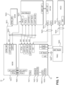
- Figure 1 is a block diagram of the conventional computing system 10, which includes a first IC 12, which may be an application processor (sometimes referred to herein as an "AP").
- the first IC 12 may include plural subsystems 14(1)-14(N), which may include navigation systems, such as global navigation satellite system (GNSS) (sometimes referred to herein as "Nav"), modems, such as a cellular modem for 3G, 4G, and/or long term evolution (LTE), sensor subsystems, Always On Processor (AOP) subsystems, audio subsystems, and the like.
- GNSS global navigation satellite system
- LTE long term evolution
- sensor subsystems such as a cellular modem for 3G, 4G, and/or long term evolution (LTE)
- AOP Always On Processor
- each subsystem of the plural subsystems 14(1)-14(N) may have a node (not illustrated) associated therewith that translates application layer activity of the subsystem to a lower layer in a protocol stack for communication with other nodes.
- the conventional computing system 10 may further include other ICs 16(1)-16(6). While six other ICs 16(1)-16(6) are illustrated, it should be appreciated that more or fewer other ICs such as the other ICs 16(1)-16(6) may be present within the conventional computing system 10.
- ICs 16(1) and 16(2) are mobile device modems (MDMs) and other IC 16(4) is a near field communication modem (NFCM) such as a WIFI or BLUETOOTH TM system (sometimes referred to as WIFI/BT).
- NFCM near field communication modem
- Other IC 16(5) may be a wireless codec device such as an audio or voice codec (sometimes referred to as WCD), and other IC 16(6) may be a power management IC (PMIC).
- PMIC power management IC
- each of the first IC 12 and the other ICs 16(1)-16(6) may be its own chip mounted on a printed circuit board (PCB) within the conventional computing system 10. Such mounting may be done by inserting pins of the chip into a socket, soldering pins to the PCB, or other techniques as is well understood.
- PCB printed circuit board
- communication bus 18(2) includes a two-wire (2W) Peripheral Component Interconnect (PCI) express (PCIe) bus, a four-wire (4W) Universal asynchronous receiver/transmitter (UART) host controller interface (UARTHCI) bus, a two-wire UART BLUETOOTH Low Energy (UART BLE) bus, and a four-wire UART mobility/mobile assisted wireless-fidelity (WiFi) connectivity (UART MAWC) bus.
- PCI Peripheral Component Interconnect
- UARTHCI Universal asynchronous receiver/transmitter
- UART BLE Universal asynchronous receiver/transmitter
- UART BLE two-wire UART BLUETOOTH Low Energy
- WiFi wireless-fidelity
- exemplary aspects of the present disclosure consolidate low-speed buses within a computing system into a single low-speed bus and implement a protocol that allows node-to-node communication both at an intrachip level and an interchip level.
- Such consolidation simplifies routing of the bus, reduces opportunities for EMI, and reduces pin counts on the chips.
- API application programming interface
- Figure 2 illustrates an exemplary computing system 30 with a first IC 32, which may be an application processor.
- the first IC 32 may include plural subsystems (shown as rectangles, but not numerically labeled).
- the subsystems may include navigation subsystems, modem subsystems, sensor subsystems, audio subsystems, AOP subsystems, and the like.
- Each of the plural subsystems has an associated node.
- the first IC 32 has nodes 34(1)-34(N). It should be appreciated that the nodes 34(1)-34(N) have respective transmitters 34(1) Tx -34(N) Tx and respective receivers 34(I) Rx -34(N) Rx .
- the first IC 32 includes a gateway 46 (also labeled "GW” in the Figures).
- the gateway 46 includes an internal interface that is coupled to the nodes 34(1)-34(N) and an external interface that is coupled to the external bus 38.
- the other ICs 36(1)-36(M) include respective gateways 48(1)-48(M) (also referred to as "GW” in the Figures) that are similar to the gateway 46.
- other buses such as a USB and PCIe bus may remain, in general, these are high-speed buses.
- low-speed buses are buses having speeds up to 50-100 Mbps.
- high-speed buses are in the 100s to 1000s of Mbps or Gbps.
- the frequency of the external bus 38 may be 57.6 MHz, which is a multiple of the common 19.2 MHz found in many cellular designs and qualifies as a low-speed bus.
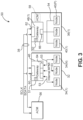
- Figure 3 provides a simplified block diagram of a partial computing system 50 extracted from the computing system 30 of Figure 2 .
- the partial computing system 50 includes the first IC 32, having a control system 51 (labeled "CS" in the Figures), the other IC 36(1), having a control system 52 (labeled "CS” in the Figures), and the external bus 38 coupling the first IC 32 and the other IC 36(1).
- the external bus 38 may be a two-wire bus capable of carrying a clock signal (SCLK) on a first wire and a data signal (SDATA) on a second wire.
- SCLK clock signal
- SDATA data signal
- the gateway 46 of the first IC 32 is coupled directly by point-to-point coupling 53) to the nodes 34(1)-34(N).
- control systems 51 and 52 are internal to the respective gateways 46 and 48(1), the present disclosure is not so limited, and the control systems 51 and 52 may be outside the respective gateways 46 and 48(1).
- one or more of the other ICs 36(1)-36(M) are activated.
- the other IC 36(1) is activated and the second gateway 48(1) boots (block 80).
- first and second are used for convenience in discriminating between the elements and are not necessarily strict temporal labels.
- the second gateway 48(1) signals the second nodes 40(1)-40(P) to register (block 82).
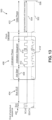
- FIG. 6 is a signal flow diagram 130 showing how a node (e.g., node 34(1)) registers with a gateway (e.g., the gateway 46) on a reset or initialization.
- the node 34(1) includes node hardware (HW) 132 and node software (SW) 134.
- the gateway 46 includes a gateway (referenced in drawings as GW) port manager 140, a gateway routing table 142 (e.g., the system topology and status table 100), a gateway external bus manager 144, and a gateway configuration SW 146.
- GW gateway routing table 142
- the node 34(1) may write a reset condition in a status register (not illustrated).
- the gateway port manager 140 sends a reset acknowledgment (ACK) 158 to the node HW 132.
- the node HW 132 sends a node-initialization interrupt 160 to the node SW 134.
- the gateway configuration SW 146 may write Logical NodeID, Valid, Reliable/Non-Reliable in the port table with signal 162.
- the gateway configuration SW 146 may be triggered by the node-initialization interrupt 160.
- the node HW 132 sets the auto-enable bit with command 164.
- the node SW 134 sends an enable node command 166 to the node HW 132.
- the node HW 132 sends a port CONF command (sometimes referred to as CMD) 168 to the gateway port manager 140, which responds with a port CONF ACK 170 and locks (write protects or "WP") the port table such that it cannot be modified by the gateway configuration SW 146.
- CMD port CONF command
- WP write protects
- the gateway routing table 142 then sends a scout command 200 with a node state change to the gateway external bus manager 144.
- the gateway port manager 140 sends a CONFDONE ACK 202 to the node HW 132 and the port table is unlocked and may be modified by the gateway configuration SW 146.
- the signals and commands 170-202 are repeated for each node ID in the port table.
- the node HW 132 ends by sending a node configuration done interrupt 204 to the node SW 134.
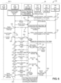
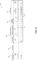
- FIG 8 is an exemplary scout message 250 according to an exemplary aspect of a protocol of the present disclosure.
- the scout message 250 may include the following fields: idle field 252, start field 254, scout identifier field 256, version ("ver") field 258, priority field 260, a handover field 262, a message header 264, and one to four scout commands 266 (only one illustrated).
- the handover field 262 ends the arbitration phase of the scout message 250 and begins the data phase.
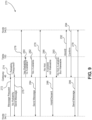
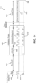
- Figure 10 is a signal diagram 310 of the node 34(1) communicating with a second remote node 40(1) on a remote IC such as one of the other ICs 36(1)-36(M).
- the node 34(1) sends a message request 312 to the gateway 46.
- the message request 312 may include attributes such as reliability requirements.
- the gateway 46 checks if reliability is required (signal 314). If no reliability is required, the gateway 46 instructs the node 34(1) to send the message (signal 316) and the node 34(1) sends the message 318 across the external bus 38 to the remote destination node 40(1).
- the gateway 46 sends a wake command 332 to the remote destination node 40(1) across the external bus 38.
- the remote destination node 40(1) sends a confirmation of waking (signal 334) across the external bus 38, and the gateway 46 instructs the node 34(1) to send the message (signal 336).
- the node 34(1) sends the message 318.
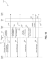
- the gateway can send a unique bus access request that will cause a system-wide reset to occur.
- the unique bus access request is referred to as a bus error halt sequence.
- the most urgent priority value in the arbitration process is reserved for transmitting the bus error halt sequence.
- this priority value can be either all-ones or all-zeros, depending on assignment of the message priority values in the computing system 30.
- the bus error halt sequence can be transmitted by any of the gateways 46 and 48(1)-48(M), and it is permissible for more than one of the gateways 46 and 48(1)-48(M) to transmit the bus error halt sequence simultaneously. It should be appreciated that by using the most urgent priority value for the bus error halt sequence, the gateway(s) 46 and 48(1)-48(M) that does transmit the bus error halt sequence will win the arbitration phase 406. The winning gateway(s) then does not transmit any data in the data phase 422. Because all winning gateway(s) do not transmit any data, there is no contention, even if there is a tie in the arbitration phase 406.
Landscapes
- Engineering & Computer Science (AREA)
- Theoretical Computer Science (AREA)
- General Engineering & Computer Science (AREA)
- Physics & Mathematics (AREA)
- General Physics & Mathematics (AREA)
- Computer Hardware Design (AREA)
- Environmental & Geological Engineering (AREA)
- Computer Networks & Wireless Communication (AREA)
- Signal Processing (AREA)
- Quality & Reliability (AREA)
- Mathematical Physics (AREA)
- Small-Scale Networks (AREA)
- Data Exchanges In Wide-Area Networks (AREA)
- Bus Control (AREA)
Applications Claiming Priority (3)
| Application Number | Priority Date | Filing Date | Title |
|---|---|---|---|
| US14/850,104 US20170075843A1 (en) | 2015-09-10 | 2015-09-10 | Unified systems and methods for interchip and intrachip node communication |
| EP16754624.1A EP3347823A1 (en) | 2015-09-10 | 2016-08-12 | Unified systems and methods for interchip and intrachip node communication |
| PCT/US2016/046728 WO2017044247A1 (en) | 2015-09-10 | 2016-08-12 | Unified systems and methods for interchip and intrachip node communication |
Related Parent Applications (1)
| Application Number | Title | Priority Date | Filing Date |
|---|---|---|---|
| EP16754624.1A Division EP3347823A1 (en) | 2015-09-10 | 2016-08-12 | Unified systems and methods for interchip and intrachip node communication |
Publications (3)
| Publication Number | Publication Date |
|---|---|
| EP4195058A1 EP4195058A1 (en) | 2023-06-14 |
| EP4195058B1 true EP4195058B1 (en) | 2024-07-03 |
| EP4195058C0 EP4195058C0 (en) | 2024-07-03 |
Family
ID=56787712
Family Applications (2)
| Application Number | Title | Priority Date | Filing Date |
|---|---|---|---|
| EP23154234.1A Active EP4195058B1 (en) | 2015-09-10 | 2016-08-12 | Unified systems and methods for interchip and intrachip node communication |
| EP16754624.1A Ceased EP3347823A1 (en) | 2015-09-10 | 2016-08-12 | Unified systems and methods for interchip and intrachip node communication |
Family Applications After (1)
| Application Number | Title | Priority Date | Filing Date |
|---|---|---|---|
| EP16754624.1A Ceased EP3347823A1 (en) | 2015-09-10 | 2016-08-12 | Unified systems and methods for interchip and intrachip node communication |
Country Status (7)
| Country | Link |
|---|---|
| US (2) | US20170075843A1 (enExample) |
| EP (2) | EP4195058B1 (enExample) |
| JP (1) | JP6845224B2 (enExample) |
| KR (2) | KR102704511B1 (enExample) |
| CN (1) | CN108027792B (enExample) |
| BR (1) | BR112018004715A2 (enExample) |
| WO (1) | WO2017044247A1 (enExample) |
Families Citing this family (8)
| Publication number | Priority date | Publication date | Assignee | Title |
|---|---|---|---|---|
| US20170075843A1 (en) | 2015-09-10 | 2017-03-16 | Qualcomm Incorporated | Unified systems and methods for interchip and intrachip node communication |
| US10521392B2 (en) | 2017-05-10 | 2019-12-31 | Qualcomm Incorporated | Slave master-write/read datagram payload extension |
| US20190227971A1 (en) * | 2018-01-23 | 2019-07-25 | Qualcomm Incorporated | Architecture for consolidating multiple sources of low-bandwidth data over a serial bus |
| US11443713B2 (en) * | 2020-01-30 | 2022-09-13 | Apple Inc. | Billboard for context information sharing |
| CN113296479B (zh) * | 2020-06-17 | 2024-07-23 | 盒马(中国)有限公司 | 总线入网单元、输送线电气控制系统及部署方法 |
| US11675713B2 (en) | 2021-04-02 | 2023-06-13 | Micron Technology, Inc. | Avoiding deadlock with a fabric having multiple systems on chip |
| JP2024120116A (ja) * | 2021-05-10 | 2024-09-04 | 日本たばこ産業株式会社 | エアロゾル生成装置の回路ユニット及びエアロゾル生成装置 |
| CN115460128B (zh) * | 2022-11-09 | 2023-07-07 | 之江实验室 | 一种面向多芯粒组合芯片的片上网络仿真系统 |
Family Cites Families (34)
| Publication number | Priority date | Publication date | Assignee | Title |
|---|---|---|---|---|
| US5199106A (en) * | 1986-09-19 | 1993-03-30 | International Business Machines Corporation | Input output interface controller connecting a synchronous bus to an asynchronous bus and methods for performing operations on the bus |
| JPS63211837A (ja) * | 1987-02-27 | 1988-09-02 | Hitachi Ltd | デ−タ伝送制御方式 |
| JP2544481B2 (ja) * | 1988-06-20 | 1996-10-16 | 株式会社日立製作所 | 通信制御方式 |
| US6157967A (en) | 1992-12-17 | 2000-12-05 | Tandem Computer Incorporated | Method of data communication flow control in a data processing system using busy/ready commands |
| US6247161B1 (en) | 1997-01-16 | 2001-06-12 | Advanced Micro Devices, Inc. | Dynamically configured on-chip communications paths based on statistical analysis |
| US6173350B1 (en) * | 1997-10-17 | 2001-01-09 | Eveready Battery Company Inc. | System and method for writing data to a serial bus from a smart battery |
| US6714994B1 (en) | 1998-12-23 | 2004-03-30 | Advanced Micro Devices, Inc. | Host bridge translating non-coherent packets from non-coherent link to coherent packets on conherent link and vice versa |
| US6791949B1 (en) * | 2000-04-28 | 2004-09-14 | Raytheon Company | Network protocol for wireless ad hoc networks |
| JP2002051055A (ja) * | 2000-08-04 | 2002-02-15 | Sony Corp | 通信制御方法、通信システム及び通信装置 |
| US7191271B2 (en) * | 2001-09-20 | 2007-03-13 | Lockheed Martin Corporation | Two level multi-tier system bus |
| US7484118B2 (en) | 2003-12-16 | 2009-01-27 | International Business Machines Corporation | Multi nodal computer system and method for handling check stops in the multi nodal computer system |
| US7409473B2 (en) | 2004-12-21 | 2008-08-05 | Sandisk Corporation | Off-chip data relocation |
| US7751850B2 (en) | 2005-09-01 | 2010-07-06 | Broadcom Corporation | Single chip multimode baseband processing circuitry with a shared radio interface |
| US7464225B2 (en) | 2005-09-26 | 2008-12-09 | Rambus Inc. | Memory module including a plurality of integrated circuit memory devices and a plurality of buffer devices in a matrix topology |
| US20070109015A1 (en) * | 2005-11-15 | 2007-05-17 | Alcatel | Switched integrated circuit connection architectures and techniques |
| US8189573B2 (en) * | 2005-12-22 | 2012-05-29 | Intel Corporation | Method and apparatus for configuring at least one port in a switch to be an upstream port or a downstream port |
| US7945721B1 (en) * | 2006-08-11 | 2011-05-17 | Oracle America, Inc. | Flexible control and/or status register configuration |
| JP2009021939A (ja) | 2007-07-13 | 2009-01-29 | Oki Electric Ind Co Ltd | ノード情報収集システム、ネットワーク装置及びノード |
| US9009350B2 (en) | 2008-04-01 | 2015-04-14 | International Business Machines Corporation | Determining a path for network traffic between nodes in a parallel computer |
| US8140835B2 (en) | 2008-05-09 | 2012-03-20 | International Business Machines Corporation | Updating a basic input/output system (‘BIOS’) boot block security module in compute nodes of a multinode computer |
| US20090307408A1 (en) | 2008-06-09 | 2009-12-10 | Rowan Nigel Naylor | Peer-to-Peer Embedded System Communication Method and Apparatus |
| US20100158005A1 (en) | 2008-12-23 | 2010-06-24 | Suvhasis Mukhopadhyay | System-On-a-Chip and Multi-Chip Systems Supporting Advanced Telecommunication Functions |
| EP2339795B1 (en) | 2009-12-07 | 2013-08-14 | STMicroelectronics (Research & Development) Limited | Inter-chip communication interface for a multi-chip package |
| US8359367B2 (en) | 2010-01-08 | 2013-01-22 | International Business Machines Corporation | Network support for system initiated checkpoints |
| US20120166621A1 (en) | 2010-12-23 | 2012-06-28 | Anish Sharma | Sharing the Status of S-CSCF Nodes Across I-CSCF Nodes in a Communications Network |
| US8824295B2 (en) | 2011-12-30 | 2014-09-02 | Qualcomm Technologies, Inc. | Link between chips using virtual channels and credit based flow control |
| WO2013111010A1 (en) | 2012-01-27 | 2013-08-01 | Marvell World Trade Ltd. | Chip-to-chip communications |
| CA2874899C (en) * | 2012-06-01 | 2017-07-11 | Blackberry Limited | Universal synchronization engine based on probabilistic methods for guarantee of lock in multiformat audio systems |
| US20130339091A1 (en) * | 2012-06-15 | 2013-12-19 | Anthony W. Humay | Intelligent social polling platform |
| CN103838698A (zh) * | 2012-11-27 | 2014-06-04 | 鸿富锦精密工业(深圳)有限公司 | I2c总线架构及设备可用性查询方法 |
| US9152598B2 (en) | 2012-11-28 | 2015-10-06 | Atmel Corporation | Connecting multiple slave devices to a single master controller in bus system |
| US20150120826A1 (en) | 2013-10-28 | 2015-04-30 | Bernd Gauweiler | Node control in a distributed peer-to-peer network |
| US9497710B2 (en) * | 2013-11-25 | 2016-11-15 | Qualcomm Incorporated | Multipoint interface shortest pulse width priority resolution |
| US20170075843A1 (en) | 2015-09-10 | 2017-03-16 | Qualcomm Incorporated | Unified systems and methods for interchip and intrachip node communication |
-
2015
- 2015-09-10 US US14/850,104 patent/US20170075843A1/en not_active Abandoned
-
2016
- 2016-08-12 EP EP23154234.1A patent/EP4195058B1/en active Active
- 2016-08-12 CN CN201680052466.3A patent/CN108027792B/zh active Active
- 2016-08-12 KR KR1020187009926A patent/KR102704511B1/ko active Active
- 2016-08-12 KR KR1020247022151A patent/KR102853457B1/ko active Active
- 2016-08-12 BR BR112018004715A patent/BR112018004715A2/pt not_active Application Discontinuation
- 2016-08-12 WO PCT/US2016/046728 patent/WO2017044247A1/en not_active Ceased
- 2016-08-12 JP JP2018509894A patent/JP6845224B2/ja active Active
- 2016-08-12 EP EP16754624.1A patent/EP3347823A1/en not_active Ceased
-
2021
- 2021-06-30 US US17/363,407 patent/US11720512B2/en active Active
Also Published As
| Publication number | Publication date |
|---|---|
| US20170075843A1 (en) | 2017-03-16 |
| EP4195058A1 (en) | 2023-06-14 |
| JP6845224B2 (ja) | 2021-03-17 |
| KR102704511B1 (ko) | 2024-09-06 |
| KR20180050727A (ko) | 2018-05-15 |
| CN108027792A (zh) | 2018-05-11 |
| US11720512B2 (en) | 2023-08-08 |
| CN108027792B (zh) | 2021-08-20 |
| EP3347823A1 (en) | 2018-07-18 |
| WO2017044247A1 (en) | 2017-03-16 |
| KR102853457B1 (ko) | 2025-09-01 |
| JP2018528540A (ja) | 2018-09-27 |
| EP4195058C0 (en) | 2024-07-03 |
| BR112018004715A2 (pt) | 2018-09-25 |
| KR20240108580A (ko) | 2024-07-09 |
| US20210326290A1 (en) | 2021-10-21 |
Similar Documents
| Publication | Publication Date | Title |
|---|---|---|
| US11720512B2 (en) | Unified systems and methods for interchip and intrachip node communication | |
| US10521392B2 (en) | Slave master-write/read datagram payload extension | |
| CN105683936B (zh) | 具有多个从设备标识符的相机控制从设备 | |
| US10467154B2 (en) | Multi-port multi-sideband-GPIO consolidation technique over a multi-drop serial bus | |
| CN108885602A (zh) | 多协议i3c共用命令码 | |
| EP3158698B1 (en) | Systems and methods for providing power savings and interference mitigation on physical transmission media | |
| US20170364472A1 (en) | Sensors global bus | |
| CN108370338A (zh) | 用于消息接发和输入/输出传递接口的最优等待时间分组化器有限状态机 | |
| US10572410B2 (en) | Function-specific communication on a multi-drop bus for coexistence management | |
| CN104322033A (zh) | 使用第二协议的扩展功能结构来控制第一协议的物理链路 | |
| US10592441B2 (en) | Bus communication enhancement based on identification capture during bus arbitration | |
| CN104350720B (zh) | 提供用于双向串行互连的串行协议的装置、方法和系统 | |
| US10579549B2 (en) | Staggered transmissions on a multi-drop half-duplex bus | |
| US11520729B2 (en) | I2C bus architecture using shared clock and dedicated data lines | |
| TW202024931A (zh) | I3c匯流排上的緊急帶內中斷 | |
| US20190347225A1 (en) | Latency optimized i3c virtual gpio with configurable operating mode and device skip | |
| CN119816821A (zh) | 使用端口聚集提高射频前端(rffe)吞吐量 |
Legal Events
| Date | Code | Title | Description |
|---|---|---|---|
| PUAI | Public reference made under article 153(3) epc to a published international application that has entered the european phase |
Free format text: ORIGINAL CODE: 0009012 |
|
| STAA | Information on the status of an ep patent application or granted ep patent |
Free format text: STATUS: REQUEST FOR EXAMINATION WAS MADE |
|
| 17P | Request for examination filed |
Effective date: 20230131 |
|
| AC | Divisional application: reference to earlier application |
Ref document number: 3347823 Country of ref document: EP Kind code of ref document: P |
|
| AK | Designated contracting states |
Kind code of ref document: A1 Designated state(s): AL AT BE BG CH CY CZ DE DK EE ES FI FR GB GR HR HU IE IS IT LI LT LU LV MC MK MT NL NO PL PT RO RS SE SI SK SM TR |
|
| GRAP | Despatch of communication of intention to grant a patent |
Free format text: ORIGINAL CODE: EPIDOSNIGR1 |
|
| RIC1 | Information provided on ipc code assigned before grant |
Ipc: G06F 13/40 20060101AFI20231221BHEP |
|
| STAA | Information on the status of an ep patent application or granted ep patent |
Free format text: STATUS: GRANT OF PATENT IS INTENDED |
|
| INTG | Intention to grant announced |
Effective date: 20240125 |
|
| GRAS | Grant fee paid |
Free format text: ORIGINAL CODE: EPIDOSNIGR3 |
|
| GRAA | (expected) grant |
Free format text: ORIGINAL CODE: 0009210 |
|
| STAA | Information on the status of an ep patent application or granted ep patent |
Free format text: STATUS: THE PATENT HAS BEEN GRANTED |
|
| AC | Divisional application: reference to earlier application |
Ref document number: 3347823 Country of ref document: EP Kind code of ref document: P |
|
| AK | Designated contracting states |
Kind code of ref document: B1 Designated state(s): AL AT BE BG CH CY CZ DE DK EE ES FI FR GB GR HR HU IE IS IT LI LT LU LV MC MK MT NL NO PL PT RO RS SE SI SK SM TR |
|
| REG | Reference to a national code |
Ref country code: CH Ref legal event code: EP |
|
| REG | Reference to a national code |
Ref country code: DE Ref legal event code: R096 Ref document number: 602016088310 Country of ref document: DE |
|
| U01 | Request for unitary effect filed |
Effective date: 20240715 |
|
| U07 | Unitary effect registered |
Designated state(s): AT BE BG DE DK EE FI FR IT LT LU LV MT NL PT RO SE SI Effective date: 20240902 |
|
| U20 | Renewal fee for the european patent with unitary effect paid |
Year of fee payment: 9 Effective date: 20241126 |
|
| PG25 | Lapsed in a contracting state [announced via postgrant information from national office to epo] |
Ref country code: NO Free format text: LAPSE BECAUSE OF FAILURE TO SUBMIT A TRANSLATION OF THE DESCRIPTION OR TO PAY THE FEE WITHIN THE PRESCRIBED TIME-LIMIT Effective date: 20241003 |
|
| PG25 | Lapsed in a contracting state [announced via postgrant information from national office to epo] |
Ref country code: GR Free format text: LAPSE BECAUSE OF FAILURE TO SUBMIT A TRANSLATION OF THE DESCRIPTION OR TO PAY THE FEE WITHIN THE PRESCRIBED TIME-LIMIT Effective date: 20241004 Ref country code: PL Free format text: LAPSE BECAUSE OF FAILURE TO SUBMIT A TRANSLATION OF THE DESCRIPTION OR TO PAY THE FEE WITHIN THE PRESCRIBED TIME-LIMIT Effective date: 20240703 |
|
| PG25 | Lapsed in a contracting state [announced via postgrant information from national office to epo] |
Ref country code: IS Free format text: LAPSE BECAUSE OF FAILURE TO SUBMIT A TRANSLATION OF THE DESCRIPTION OR TO PAY THE FEE WITHIN THE PRESCRIBED TIME-LIMIT Effective date: 20241103 |
|
| PG25 | Lapsed in a contracting state [announced via postgrant information from national office to epo] |
Ref country code: CZ Free format text: LAPSE BECAUSE OF FAILURE TO SUBMIT A TRANSLATION OF THE DESCRIPTION OR TO PAY THE FEE WITHIN THE PRESCRIBED TIME-LIMIT Effective date: 20240703 Ref country code: HR Free format text: LAPSE BECAUSE OF FAILURE TO SUBMIT A TRANSLATION OF THE DESCRIPTION OR TO PAY THE FEE WITHIN THE PRESCRIBED TIME-LIMIT Effective date: 20240703 |
|
| PGFP | Annual fee paid to national office [announced via postgrant information from national office to epo] |
Ref country code: IE Payment date: 20241125 Year of fee payment: 9 |
|
| PG25 | Lapsed in a contracting state [announced via postgrant information from national office to epo] |
Ref country code: ES Free format text: LAPSE BECAUSE OF FAILURE TO SUBMIT A TRANSLATION OF THE DESCRIPTION OR TO PAY THE FEE WITHIN THE PRESCRIBED TIME-LIMIT Effective date: 20240703 Ref country code: RS Free format text: LAPSE BECAUSE OF FAILURE TO SUBMIT A TRANSLATION OF THE DESCRIPTION OR TO PAY THE FEE WITHIN THE PRESCRIBED TIME-LIMIT Effective date: 20241003 |
|
| PG25 | Lapsed in a contracting state [announced via postgrant information from national office to epo] |
Ref country code: RS Free format text: LAPSE BECAUSE OF FAILURE TO SUBMIT A TRANSLATION OF THE DESCRIPTION OR TO PAY THE FEE WITHIN THE PRESCRIBED TIME-LIMIT Effective date: 20241003 Ref country code: PL Free format text: LAPSE BECAUSE OF FAILURE TO SUBMIT A TRANSLATION OF THE DESCRIPTION OR TO PAY THE FEE WITHIN THE PRESCRIBED TIME-LIMIT Effective date: 20240703 Ref country code: NO Free format text: LAPSE BECAUSE OF FAILURE TO SUBMIT A TRANSLATION OF THE DESCRIPTION OR TO PAY THE FEE WITHIN THE PRESCRIBED TIME-LIMIT Effective date: 20241003 Ref country code: IS Free format text: LAPSE BECAUSE OF FAILURE TO SUBMIT A TRANSLATION OF THE DESCRIPTION OR TO PAY THE FEE WITHIN THE PRESCRIBED TIME-LIMIT Effective date: 20241103 Ref country code: HR Free format text: LAPSE BECAUSE OF FAILURE TO SUBMIT A TRANSLATION OF THE DESCRIPTION OR TO PAY THE FEE WITHIN THE PRESCRIBED TIME-LIMIT Effective date: 20240703 Ref country code: GR Free format text: LAPSE BECAUSE OF FAILURE TO SUBMIT A TRANSLATION OF THE DESCRIPTION OR TO PAY THE FEE WITHIN THE PRESCRIBED TIME-LIMIT Effective date: 20241004 Ref country code: ES Free format text: LAPSE BECAUSE OF FAILURE TO SUBMIT A TRANSLATION OF THE DESCRIPTION OR TO PAY THE FEE WITHIN THE PRESCRIBED TIME-LIMIT Effective date: 20240703 Ref country code: CZ Free format text: LAPSE BECAUSE OF FAILURE TO SUBMIT A TRANSLATION OF THE DESCRIPTION OR TO PAY THE FEE WITHIN THE PRESCRIBED TIME-LIMIT Effective date: 20240703 |
|
| REG | Reference to a national code |
Ref country code: CH Ref legal event code: PL |
|
| PG25 | Lapsed in a contracting state [announced via postgrant information from national office to epo] |
Ref country code: SM Free format text: LAPSE BECAUSE OF FAILURE TO SUBMIT A TRANSLATION OF THE DESCRIPTION OR TO PAY THE FEE WITHIN THE PRESCRIBED TIME-LIMIT Effective date: 20240703 |
|
| PG25 | Lapsed in a contracting state [announced via postgrant information from national office to epo] |
Ref country code: CH Free format text: LAPSE BECAUSE OF NON-PAYMENT OF DUE FEES Effective date: 20240831 Ref country code: MC Free format text: LAPSE BECAUSE OF FAILURE TO SUBMIT A TRANSLATION OF THE DESCRIPTION OR TO PAY THE FEE WITHIN THE PRESCRIBED TIME-LIMIT Effective date: 20240703 |
|
| PG25 | Lapsed in a contracting state [announced via postgrant information from national office to epo] |
Ref country code: SK Free format text: LAPSE BECAUSE OF FAILURE TO SUBMIT A TRANSLATION OF THE DESCRIPTION OR TO PAY THE FEE WITHIN THE PRESCRIBED TIME-LIMIT Effective date: 20240703 |
|
| PLBE | No opposition filed within time limit |
Free format text: ORIGINAL CODE: 0009261 |
|
| STAA | Information on the status of an ep patent application or granted ep patent |
Free format text: STATUS: NO OPPOSITION FILED WITHIN TIME LIMIT |
|
| 26N | No opposition filed |
Effective date: 20250404 |
|
| U20 | Renewal fee for the european patent with unitary effect paid |
Year of fee payment: 10 Effective date: 20250710 |
|
| PGFP | Annual fee paid to national office [announced via postgrant information from national office to epo] |
Ref country code: GB Payment date: 20250710 Year of fee payment: 10 |