EP4192206B1 - Leiterplattenanordnung und elektronische vorrichtung - Google Patents
Leiterplattenanordnung und elektronische vorrichtung Download PDFInfo
- Publication number
- EP4192206B1 EP4192206B1 EP22859527.8A EP22859527A EP4192206B1 EP 4192206 B1 EP4192206 B1 EP 4192206B1 EP 22859527 A EP22859527 A EP 22859527A EP 4192206 B1 EP4192206 B1 EP 4192206B1
- Authority
- EP
- European Patent Office
- Prior art keywords
- support portion
- pads
- circuit board
- support
- board assembly
- Prior art date
- Legal status (The legal status is an assumption and is not a legal conclusion. Google has not performed a legal analysis and makes no representation as to the accuracy of the status listed.)
- Active
Links
Images





Classifications
-
- H—ELECTRICITY
- H05—ELECTRIC TECHNIQUES NOT OTHERWISE PROVIDED FOR
- H05K—PRINTED CIRCUITS; CASINGS OR CONSTRUCTIONAL DETAILS OF ELECTRIC APPARATUS; MANUFACTURE OF ASSEMBLAGES OF ELECTRICAL COMPONENTS
- H05K1/00—Printed circuits
- H05K1/02—Details
- H05K1/14—Structural association of two or more printed circuits
- H05K1/144—Stacked arrangements of planar printed circuit boards
-
- H—ELECTRICITY
- H05—ELECTRIC TECHNIQUES NOT OTHERWISE PROVIDED FOR
- H05K—PRINTED CIRCUITS; CASINGS OR CONSTRUCTIONAL DETAILS OF ELECTRIC APPARATUS; MANUFACTURE OF ASSEMBLAGES OF ELECTRICAL COMPONENTS
- H05K7/00—Constructional details common to different types of electric apparatus
- H05K7/14—Mounting supporting structure in casing or on frame or rack
- H05K7/1422—Printed circuit boards receptacles, e.g. stacked structures, electronic circuit modules or box like frames
-
- H—ELECTRICITY
- H01—ELECTRIC ELEMENTS
- H01R—ELECTRICALLY-CONDUCTIVE CONNECTIONS; STRUCTURAL ASSOCIATIONS OF A PLURALITY OF MUTUALLY-INSULATED ELECTRICAL CONNECTING ELEMENTS; COUPLING DEVICES; CURRENT COLLECTORS
- H01R12/00—Structural associations of a plurality of mutually-insulated electrical connecting elements, specially adapted for printed circuits, e.g. printed circuit boards [PCB], flat or ribbon cables, or like generally planar structures, e.g. terminal strips, terminal blocks; Coupling devices specially adapted for printed circuits, flat or ribbon cables, or like generally planar structures; Terminals specially adapted for contact with, or insertion into, printed circuits, flat or ribbon cables, or like generally planar structures
- H01R12/50—Fixed connections
- H01R12/51—Fixed connections for rigid printed circuits or like structures
- H01R12/52—Fixed connections for rigid printed circuits or like structures connecting to other rigid printed circuits or like structures
-
- H—ELECTRICITY
- H05—ELECTRIC TECHNIQUES NOT OTHERWISE PROVIDED FOR
- H05K—PRINTED CIRCUITS; CASINGS OR CONSTRUCTIONAL DETAILS OF ELECTRIC APPARATUS; MANUFACTURE OF ASSEMBLAGES OF ELECTRICAL COMPONENTS
- H05K1/00—Printed circuits
- H05K1/02—Details
-
- H—ELECTRICITY
- H05—ELECTRIC TECHNIQUES NOT OTHERWISE PROVIDED FOR
- H05K—PRINTED CIRCUITS; CASINGS OR CONSTRUCTIONAL DETAILS OF ELECTRIC APPARATUS; MANUFACTURE OF ASSEMBLAGES OF ELECTRICAL COMPONENTS
- H05K1/00—Printed circuits
- H05K1/02—Details
- H05K1/0213—Electrical arrangements not otherwise provided for
-
- H—ELECTRICITY
- H05—ELECTRIC TECHNIQUES NOT OTHERWISE PROVIDED FOR
- H05K—PRINTED CIRCUITS; CASINGS OR CONSTRUCTIONAL DETAILS OF ELECTRIC APPARATUS; MANUFACTURE OF ASSEMBLAGES OF ELECTRICAL COMPONENTS
- H05K3/00—Apparatus or processes for manufacturing printed circuits
- H05K3/30—Assembling printed circuits with electric components, e.g. with resistors
- H05K3/32—Assembling printed circuits with electric components, e.g. with resistors electrically connecting electric components or wires to printed circuits
- H05K3/34—Assembling printed circuits with electric components, e.g. with resistors electrically connecting electric components or wires to printed circuits by soldering
- H05K3/341—Surface mounted components
-
- H—ELECTRICITY
- H05—ELECTRIC TECHNIQUES NOT OTHERWISE PROVIDED FOR
- H05K—PRINTED CIRCUITS; CASINGS OR CONSTRUCTIONAL DETAILS OF ELECTRIC APPARATUS; MANUFACTURE OF ASSEMBLAGES OF ELECTRICAL COMPONENTS
- H05K3/00—Apparatus or processes for manufacturing printed circuits
- H05K3/36—Assembling printed circuits with other printed circuits
- H05K3/368—Assembling printed circuits with other printed circuits parallel to each other
-
- H—ELECTRICITY
- H05—ELECTRIC TECHNIQUES NOT OTHERWISE PROVIDED FOR
- H05K—PRINTED CIRCUITS; CASINGS OR CONSTRUCTIONAL DETAILS OF ELECTRIC APPARATUS; MANUFACTURE OF ASSEMBLAGES OF ELECTRICAL COMPONENTS
- H05K1/00—Printed circuits
- H05K1/02—Details
- H05K1/11—Printed elements for providing electric connections to or between printed circuits
- H05K1/115—Via connections; Lands around holes or via connections
- H05K1/116—Lands, clearance holes or other lay-out details concerning the surrounding of a via
-
- H—ELECTRICITY
- H05—ELECTRIC TECHNIQUES NOT OTHERWISE PROVIDED FOR
- H05K—PRINTED CIRCUITS; CASINGS OR CONSTRUCTIONAL DETAILS OF ELECTRIC APPARATUS; MANUFACTURE OF ASSEMBLAGES OF ELECTRICAL COMPONENTS
- H05K2201/00—Indexing scheme relating to printed circuits covered by H05K1/00
- H05K2201/04—Assemblies of printed circuits
- H05K2201/042—Stacked spaced PCBs; Planar parts of folded flexible circuits having mounted components in between or spaced from each other
-
- H—ELECTRICITY
- H05—ELECTRIC TECHNIQUES NOT OTHERWISE PROVIDED FOR
- H05K—PRINTED CIRCUITS; CASINGS OR CONSTRUCTIONAL DETAILS OF ELECTRIC APPARATUS; MANUFACTURE OF ASSEMBLAGES OF ELECTRICAL COMPONENTS
- H05K2201/00—Indexing scheme relating to printed circuits covered by H05K1/00
- H05K2201/10—Details of components or other objects attached to or integrated in a printed circuit board
- H05K2201/10227—Other objects, e.g. metallic pieces
- H05K2201/10378—Interposers
-
- H—ELECTRICITY
- H05—ELECTRIC TECHNIQUES NOT OTHERWISE PROVIDED FOR
- H05K—PRINTED CIRCUITS; CASINGS OR CONSTRUCTIONAL DETAILS OF ELECTRIC APPARATUS; MANUFACTURE OF ASSEMBLAGES OF ELECTRICAL COMPONENTS
- H05K2201/00—Indexing scheme relating to printed circuits covered by H05K1/00
- H05K2201/20—Details of printed circuits not provided for in H05K2201/01 - H05K2201/10
- H05K2201/2036—Permanent spacer or stand-off in a printed circuit or printed circuit assembly
-
- Y—GENERAL TAGGING OF NEW TECHNOLOGICAL DEVELOPMENTS; GENERAL TAGGING OF CROSS-SECTIONAL TECHNOLOGIES SPANNING OVER SEVERAL SECTIONS OF THE IPC; TECHNICAL SUBJECTS COVERED BY FORMER USPC CROSS-REFERENCE ART COLLECTIONS [XRACs] AND DIGESTS
- Y02—TECHNOLOGIES OR APPLICATIONS FOR MITIGATION OR ADAPTATION AGAINST CLIMATE CHANGE
- Y02E—REDUCTION OF GREENHOUSE GAS [GHG] EMISSIONS, RELATED TO ENERGY GENERATION, TRANSMISSION OR DISTRIBUTION
- Y02E60/00—Enabling technologies; Technologies with a potential or indirect contribution to GHG emissions mitigation
- Y02E60/10—Energy storage using batteries
Definitions
- Embodiments of this application relate to the field of terminal technologies, and in particular, to a circuit board assembly and an electronic device.
- a plurality of circuit boards are usually stacked to provide a larger arrangement space for a battery and other functional modules in the electronic devices.
- electronic components may be scattered on the circuit boards. In this way, all the electronic components can be arranged without increasing areas of the circuit boards that bear the electronic components.
- circuit board assembly In the manner of stacking a plurality of circuit boards, two adjacent circuit boards are connected by using a frame plate.
- the frame plate and the circuit boards are assembled to form a circuit board assembly.
- Different circuit boards may be electrically connected to each other by using a frame plate to implement data information exchange.
- the circuit boards may be electrically connected to the frame plate by using solder joints.
- the solder joints also play a function of mechanical connection and fastening, to provide connection forces between the circuit boards and the frame plate.
- solder joints also play a function of mechanical connection and fastening, to provide connection forces between the circuit boards and the frame plate.
- a connection joint at which the circuit board and the frame plate are connected by using solder joints is prone to a facture. Consequently, the circuit board and the frame plate are separated, and the circuit board assembly malfunctions or fails.
- Document CN 210 670 769 discloses a circuit board assembly comprising an annular adapter board and two circuit boards arranged on two sides of the adapter board. The distance between the adapter board and each of the circuit boards is determined by a height structure that is provided on the adapter board.
- Embodiments of this application provide a circuit board assembly and an electronic device, which can ensure that a large solder joint is formed between two connected pads. This is conducive to improving connection strength between the pads.
- the first support portion and the second support portion are stacked along a thickness direction of the frame plate.
- the first support portion is connected to the frame body.
- the second support portion is connected to the board body.
- Solder joints are provided between the first pads and the second pads. The solder joints connect the first pads to the second pads.
- solder paste is printed on the first pads on the frame plate in advance, and then the circuit boards each are placed on one side of the frame plate.
- Each of the circuit boards is supported by the support bodies, so that the predetermined spacing can be maintained between the second pads on the circuit board and the first pads on the frame plate.
- the circuit board is limited by the support bodies. Therefore, the circuit board does not move close to the frame plate under the action of its own gravity, so that the predetermined spacing can still be maintained between the first pads and the second pads.
- the frame body is an annular structure.
- Two or more support bodies are spaced along a circumferential direction of the frame body. Supporting each of the circuit boards by a plurality of support bodies is conducive to ensuring that a uniform spacing is maintained between the second pads provided at different locations on the circuit board and the first pads on the frame plate.
- two or more support bodies are evenly distributed along the circumferential direction of the frame body.
- a support force applied by each support body to the circuit board is more balanced and uniform. This reduces a possibility that the circuit board inclines when being subject to an unbalanced support force, and is conducive to ensuring that the spacing between the first pads on the frame plate and the second pads on the circuit board tends to be uniform.
- both the first support portion and the second support portion are first solder resist ink layers.
- the first support portion has a uniform thickness
- the second support portion has a uniform thickness. This facilitates printing of the first solder resist ink layer with the uniform thickness on the frame body or the board body by using a printing process, thereby reducing difficulty in manufacturing the first support portion and the second support portion.
- the thickness of the first support portion is equal to the thickness of the second support portion. This facilitates printing and forming of the first solder resist ink layer with the same thickness on the frame body or the board body by using a printed board with a same thickness, thereby reducing an operation of replacing the printed board, and reducing production difficulty and production costs.
- the support body further includes a third support portion and a fourth support portion.
- the first support portion, the second support portion, the third support portion, and the fourth support portion are stacked.
- the third support portion is provided on a surface of the first support portion that faces the second support portion
- the fourth support portion is provided on a surface of the second support portion that faces the first support portion.
- both the third support portion and the fourth support portion are solder resist layers.
- the solder paste is heated and melted, the third support portion and the fourth support portion are not easily melted. This reduces a possibility that the circuit board moves close to the frame plate because the third support portion and the fourth support portion are melted and lose their support functions.
- both the third support portion and the fourth support portion are second solder resist ink layers.
- both the third support portion and the fourth support portion are insulating sheets.
- a sum of thicknesses of the first support portion and the third support portion is equal to a sum of thicknesses of the second support portion and the fourth support portion.
- the third support portion has a uniform thickness
- the fourth support portion has a uniform thickness. This can facilitate printing of the second solder resist ink layer with the uniform thickness on the frame body or the board body by using a printing process to form the third support portion or the fourth support portion, thereby reducing difficulty in manufacturing the third support portion and the fourth support portion.
- insulating sheets with a predetermined thickness are pre-processed and pre-manufactured by finish machining.
- the thickness of the third support portion is equal to the thickness of the fourth support portion. This facilitates printing and forming of the second solder resist ink layer on the frame body or the board body by using a printed board with a same thickness, or insulating sheets with a predetermined thickness can be pre-processed and pre-manufactured by finish machining, thereby reducing a possibility of complex processing operations and high production costs caused by a need of processing insulating sheets with two different thicknesses to form the third support portion and the fourth support portion.
- the frame plate further includes third pads.
- the third pads are provided on the frame body.
- the third pads each are covered by the first support portion.
- the third pads can play a function of positioning references, to help quickly and accurately provide the first support portions at predetermined locations of the frame body. This ensures that the first support portions are located at the predetermined locations, reduces a possibility that support areas between the first support portions and the second support portions become smaller due to misalignment with the second support portions that is resulted from deviation of the first support portions from the predetermined locations, and is also conducive to reducing production difficulty and improving production efficiency.
- the circuit board further includes fourth pads.
- the third pads face the fourth pads.
- the fourth pads each are covered by the second support portion.
- the fourth pads can play a function of positioning references, to help quickly and accurately provide the second support portions at predetermined locations of the board body. This ensures that the second support portions are located at the predetermined locations, reduces a possibility that support areas between the first support portions and the second support portions become smaller due to misalignment with the first support portions that is resulted from deviation of the second support portions from the predetermined locations, and is also conducive to reducing production difficulty and improving production efficiency.
- a surface of the first pad that faces the second pad is flush with a surface of the third pad that faces the fourth pad, and a surface of the second pad that faces the first pad is flush with a surface of the fourth pad that faces the third pad.
- the spacing between the first pads and the second pads can be accurately controlled by controlling the thicknesses of the first support portions and the second support portions.
- a second aspect of the embodiments of this application provides an electronic device, including the circuit board assembly described above.
- the circuit board assembly includes at least a frame plate, circuit boards, support bodies, and solder joints.
- the frame plate includes a frame body and first pads. The first pads are provided on the frame body.
- the circuit boards each are provided on one side of the frame plate.
- the circuit board includes a board body and second pads. The second pads are provided on the board body. The first pads face the second pads.
- the support bodies are provided between the frame plate and the circuit boards. The support bodies are configured to support the circuit boards, so that a predetermined spacing exists between the first pads and the second pads.
- the support bodies each include a first support portion and a second support portion. The first support portion and the second support portion are stacked along a thickness direction of the frame plate. The first support portion is connected to the frame body. The second support portion is connected to the board body. Solder joints are provided between the first pads and the second pads. The solder joints connect the first pads to the second pads.
- the frame body is an annular structure.
- Two or more support bodies are spaced along a circumferential direction of the frame body. Supporting each of the circuit boards by a plurality of support bodies is conducive to ensuring that a uniform spacing is maintained between the second pads provided at different locations on the circuit board and the first pads on the frame plate.
- two or more support bodies are evenly distributed along the circumferential direction of the frame body.
- a support force applied by each support body to the circuit board is more balanced and uniform. This reduces a possibility that the circuit board inclines when being subject to an unbalanced support force, and is conducive to ensuring that the spacing between the first pads on the frame plate and the second pads on the circuit board tends to be uniform.
- both the first support portion and the second support portion are solder resist layers.
- the solder paste is heated and melted, the first support portion and the second support portion are not easily melted. This reduces a possibility that the circuit board moves close to the frame plate because the first support portion and the second support portion are melted and lose their support functions.
- both the first support portion and the second support portion are first solder resist ink layers.
- the first support portion has a uniform thickness
- the second support portion has a uniform thickness. This facilitates printing of the first solder resist ink layer with the uniform thickness on the frame body or the board body by using a printing process, thereby reducing difficulty in manufacturing the first support portion and the second support portion.
- the thickness of the first support portion is equal to the thickness of the second support portion. This facilitates printing and forming of the first solder resist ink layer with the same thickness on the frame body or the board body by using a printed board with a same thickness, thereby reducing an operation of replacing the printed board, and reducing production difficulty and production costs.
- the support body further includes a third support portion and a fourth support portion.
- the first support portion, the second support portion, the third support portion, and the fourth support portion are stacked.
- the third support portion is provided on a surface of the first support portion that faces the second support portion
- the fourth support portion is provided on a surface of the second support portion that faces the first support portion.
- both the third support portion and the fourth support portion are solder resist layers.
- the solder paste is heated and melted, the third support portion and the fourth support portion are not easily melted. This reduces a possibility that the circuit board moves close to the frame plate because the third support portion and the fourth support portion are melted and lose their support functions.
- both the third support portion and the fourth support portion are second solder resist ink layers.
- both the third support portion and the fourth support portion are insulating sheets.
- a sum of thicknesses of the first support portion and the third support portion is equal to a sum of thicknesses of the second support portion and the fourth support portion.
- the third support portion has a uniform thickness
- the fourth support portion has a uniform thickness. This can facilitate printing of the second solder resist ink layer with the uniform thickness on the frame body or the board body by using a printing process to form the third support portion or the fourth support portion, thereby reducing difficulty in manufacturing the third support portion and the fourth support portion.
- insulating sheets with a predetermined thickness are pre-processed and pre-manufactured by finish machining.
- the thickness of the third support portion is equal to the thickness of the fourth support portion. This facilitates printing and forming of the second solder resist ink layer on the frame body or the board body by using a printed board with a same thickness, or insulating sheets with a predetermined thickness can be pre-processed and pre-manufactured by finish machining, thereby reducing a possibility of complex processing operations and high production costs caused by a need of processing insulating sheets with two different thicknesses to form the third support portion and the fourth support portion.
- the frame plate further includes third pads.
- the third pads are provided on the frame body.
- the third pads each are covered by the first support portion.
- the third pads can play a function of positioning references, to help quickly and accurately provide the first support portions at predetermined locations of the frame body. This ensures that the first support portions are located at the predetermined locations, reduces a possibility that support areas between the first support portions and the second support portions become smaller due to misalignment with the second support portions that is resulted from deviation of the first support portions from the predetermined locations, and is also conducive to reducing production difficulty and improving production efficiency.
- the circuit board further includes fourth pads.
- the third pads face the fourth pads.
- the fourth pads each are covered by the second support portion.
- the fourth pads can play a function of positioning references, to help quickly and accurately provide the second support portions at predetermined locations of the board body. This ensures that the second support portions are located at the predetermined locations, reduces a possibility that support areas between the first support portions and the second support portions become smaller due to misalignment with the first support portions that is resulted from deviation of the second support portions from the predetermined locations, and is also conducive to reducing production difficulty and improving production efficiency.
- a surface of the first pad that faces the second pad is flush with a surface of the third pad that faces the fourth pad, and a surface of the second pad that faces the first pad is flush with a surface of the fourth pad that faces the third pad.
- the spacing between the first pads and the second pads can be accurately controlled by controlling the thicknesses of the first support portions and the second support portions.
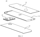
- FIG. 1 schematically shows a structure of an electronic device 10 according to an embodiment.
- an embodiment of this application provides the electronic device 10.
- the electronic device 10 may be a mobile terminal, a fixed terminal, or a foldable device, such as a monitor, a handheld wireless communication device, a desktop computer, a laptop (laptop) computer, a tablet (Tablet) computer, an ultra-mobile personal computer (UMPC), a handheld computer, a walkie-talkie, a netbook, a POS machine, or a personal digital assistant (personal digital assistant, PDA).
- UMPC ultra-mobile personal computer
- PDA personal digital assistant
- the handheld wireless communication device 10 may be a mobile phone.
- the circuit board 41 in this application may be a printed circuit board (Printed Circuit Board, PCB), a flexible printed circuit (Flexible Printed Circuit, FPC), or an integrated circuit (or referred to as a chip).
- the circuit board 41 may be a single-sided board or double-sided board.
- Single-sided board means that the electronic components 60 are provided on one side of the circuit board 41.
- Double-sided board means that the electronic components 60 are provided on both sides of the circuit board 41.
- the circuit board 41 may be a radio frequency (radio frequency, RF) board or an application processor (application processor, AP) board.
- the circuit board 41 may have a large lateral size, so that one circuit board 41 may be selected for use and a fixed quantity of electronic components 60 may be provided on the circuit board 41.
- the lateral size refers to a size measured along a direction perpendicular to the thickness direction of the electronic device 10. If the quantity and volumes of the electronic components 60 are large, a structure of the circuit board assembly 40 needs to be optimized when not all of the electronic components 60 can be accommodated on one circuit board 41. For example, a plurality of the circuit boards 41 are stacked along the thickness direction of the electronic device 10, and the electronic components 60 are provided on different circuit boards 41. In this way, an internal space of the electronic device 10 can be fully utilized along the thickness direction of the electronic device 10 to accommodate more and larger electronic components 60.
- FIG. 3 schematically shows a breakdown structure of the circuit board assembly 40 in a related technology.
- FIG. 4 schematically shows a partial cross-sectional structure of the circuit board assembly 40 shown in FIG. 3 .
- the circuit board assembly 40 includes the circuit boards 41 and a frame plate 42. Two circuit boards 41 and the frame plate 42 are stacked along a thickness direction X of the frame plate 42. The frame plate 42 is provided between the two circuit boards 41. The two circuit boards 41 are separately connected to the frame plate 42, so that a predetermined distance is maintained between the two circuit boards 41 and locations of the two circuit boards 41 do not interfere with each other.
- the two circuit boards 41 may also be electrically connected to each other by using the frame plate 42, so that data information can be mutually transmitted between the two circuit boards 41.
- the frame plate 42 has an annular structure as a whole, so that the frame plate 42 includes a middle accommodating hole 42a.
- the frame plate 42 may have a polygonal structure, such as a rectangular structure.
- the frame plate 42 includes a frame body 421 and first pads 422.
- the frame body 421 is an annular structure.
- the frame body 421 has the intermediate accommodating hole 42a.
- the first pads 422 are provided on the frame body 421.
- a material of the first pads 422 may be copper or a copper alloy.
- the circuit board 41 includes a board body 411 and second pads 412.
- the second pads 412 are provided on the board body 411.
- the first pads 422 face the second pads 412, so that locations of the first pads 422 mutually correspond to locations of the second pads 412.
- Solder joints are located between the first pads 422 and the second pads 412. The solder joints connect the first pads 422 to the second pads 412.
- a shape of the solder joint may be but is not limited to a spherical shape, an ellipsoidal shape, a cylindrical shape, or a truncated-cone shape.
- the first pads 422 include functional pads and non-functional pads.
- the functional pads can play an electrical connection function and a mechanical fastening function. After the two circuit boards 41 are connected to the frame plate 42, the two circuit boards 41 can transmit electrical signals to each other by using the functional pads.
- the non-functional pads can play a mechanical fastening function, but the two circuit boards 41 cannot transmit electrical signals to each other by using the non-functional pads.
- solder paste is printed on the first pads 422 in advance.
- the solder paste may include tin and a solder flux.
- the circuit boards 41 each are provided on one side of the frame plate 42 and made to reach contact with the solder paste.
- the solder paste is heated and melted, so that the first pads 422 and the second pads 412 are all connected to the molten solder paste.
- solder joints 70 are formed, so that the circuit boards 41 are connected to the frame plate 42 by using the solder joints 70.
- the molten solder paste heated has fluidity.
- the circuit board 41 and the frame plate 42 each have specific mass, after the solder paste is melted, the circuit board 41 moves close to the frame plate 42 under the action of its own gravity. Therefore, a spacing between the first pads 422 of the frame plate 42 and the second pads 412 of the circuit board 41 is reduced, and the first pads 422 and the second pads 412 squeeze the molten solder paste. As a result, the solder paste is squeezed, and a remaining amount of the solder paste is small. When remaining solder paste between the first pads 422 and the second pads 412 is little, the solder joints 70 formed after the solder paste is cured are small in size.
- connection force refers to a force that needs to be overcome for the pads to be separated from the solder joints.
- the force required for separating the pads from the solder joints refers to a tensile stress, along a direction away from the solder joints, that is applied to the pads along the thickness direction X and that is required for separating the pads from the solder joints. Therefore, in a scenario with an uneven force, such as a drop or a collision, a connection joint at which the circuit board 41 and the frame plate 42 are connected by using the solder joints 70 is prone to a facture.
- the circuit board 41 and the frame plate 42 are separated, and the circuit board assembly 40 malfunctions or fails.
- the solder paste that overflows from between the first pads 422 and the second pads 412 flows between two adjacent first pads 422 or between two adjacent second pads 412. This leads to a short circuit between the two first pads 422 or between the two second pads 412, thereby causing the circuit board assembly 40 to be scrapped.
- circuit board assembly 40 provided in this embodiment of this application.
- FIG. 5 schematically shows a partial cross-sectional structure of the circuit board assembly 40 according to an embodiment of this application.
- the circuit board assembly 40 in this embodiment of this application is used in the electronic device 10.
- the circuit board assembly 40 includes circuit boards 41, a frame plate 42, support bodies 43, and solder joints 70.
- the frame plate 42 includes a frame body 421 and first pads 422.
- the frame body 421 is an annular structure, and therefore forms an intermediate accommodating hole 42a.
- a material of the frame body 421 is an insulating material such as phenolic resin, epoxy resin, or polytetrafluoroethylene.
- the first pads 422 are provided on the frame body 421.
- the circuit boards 41 each are provided on one side of the frame plate 42.
- the circuit board 41 includes a board body 411 and second pads 412.
- a material of the board body 411 is an insulating material such as phenolic resin, epoxy resin, or polytetrafluoroethylene.
- Electronic components may be provided on the board body 411.
- the second pads 412 are provided on the board body 411, and the first pads 422 face the second pads 412. A quantity of the first pads 422 may be equal to a quantity of the second pads 412.
- the support bodies 43 are provided between the circuit boards 41 and the frame plate 42, so that a predetermined spacing L exists between the first pads 422 and the second pads 412.
- a predetermined spacing L exists between the first pads 422 and the second pads 412 means that the spacing between the first pads 422 and the second pads 412 can allow a proper solder paste melting space to be formed between the first pads 422 and the second pads 412, so as to ensure that the first pads 422 and the second pads 412 are both in contact with the solder paste, without squeezing the solder paste out from between the first pads 422 and the second pads 412.
- FIG. 7 schematically shows a top-view structure of the frame plate 42 according to an embodiment of this application.
- the support bodies 43 are provided between the frame plate 42 and the circuit boards 41.
- the support bodies 43 are configured to support the circuit boards 41, so that the predetermined spacing L exists between the first pads 422 and the second pads 412.
- the support bodies 43 each include a first support portion 431 and a second support portion 432.
- the first support portion 431 and the second support portion 432 are stacked along a thickness direction X of the frame plate 42.
- the first support portion 431 is connected to the frame body 421, and the second support portion 432 is connected to the board body 411 of the circuit board 41.
- the first support portion 431 and the second support portion 432 are separately provided.
- the stacked first support portion 431 and second support portion 432 can support the circuit board 41.
- the solder joints 70 are provided between the first pads 422 and the second pads 412. The solder joints 70 connect the first pads 422 to the second pads 412.
- the solder paste is printed on the first pads 422 on the frame plate 42 in advance, and then the circuit boards 41 each are placed on one side of the frame plate 42.
- Each of the circuit boards 41 is supported by the support bodies 43, so that the predetermined spacing L can be maintained between the second pads 412 on the circuit board 41 and the first pads 422 on the frame plate 42.
- the circuit board 41 is limited by the support bodies 43. Therefore, the circuit board 41 does not move close to the frame plate 42 under the action of its own gravity, so that the predetermined spacing L can still be maintained between the first pads 422 and the second pads 412.
- the first pads 422 and the second pads 412 do not squeeze the molten solder paste, and therefore the molten solder paste does not easily overflow from the space between the first pads 422 and the second pads 412.
- the molten solder paste forms the solder joints 70 after being cured. Because the solder joints 70 are large in size, the connection force between the first pads 422 and the solder joints 70 and the connection force between the second pads 412 and the solder joints 70 are large. This effectively reduces a possibility of separation between the first pads 422 and the solder joints 70 or between the second pads 412 and the solder joints 70 in a scenario with an uneven force, for example, the circuit board assembly 40 drops or collides.
- the molten solder paste does not easily overflow from the space between the first pads 422 and the second pads 412. This can also effectively reduce a possibility that a short circuit occurs between two first pads 422 or two second pads 412 due to solder paste flowing between the two first pads 422 or the two second pads 412. This is conducive to increasing a yield of the circuit board assembly 40.
- a surface of the first support portion 431 that faces the second support portion 432 and a surface of the second support portion 432 that faces the first support portion 431 come into contact with each other.
- the first support portion 431 may be connected to the frame body 421 in advance, and the second support portion 432 may be connected to the board body 411 of the circuit board 41 in advance.
- the circuit board 41 is placed on one side of the frame plate 42, and the second support portion 432 on the board body 411 of the circuit board 41 is made corresponding to the first support portion 431 on the frame body 421, and the first pads 422 are made corresponding to the second pads 412.
- the first support portion 431 abuts against the second support portion 432, so that the first support portion 431 and the second support portion 432 play a supporting function.
- two or more support bodies 43 are spaced along a circumferential direction of the frame body 421.
- the circumferential direction of the frame body 421 refers to a direction around the middle accommodating hole 42a.
- the two or more support bodies 43 can support the circuit board 41 at different locations.
- a plurality of first pads 422 and an equal quantity of corresponding second pads 412 may be provided between two adjacent support bodies 43. Supporting each of the circuit boards 41 by a plurality of support bodies 43 is conducive to ensuring that a uniform spacing is maintained between the second pads 412 provided at different locations on the circuit board 41 and the first pads 422 on the frame plate 42. This is conducive to ensuring consistency of sizes and dimensions of the solder joints 70 formed between the frame plate 42 and different regions of the circuit board 41.
- FIG. 8a schematically shows a top-view structure of the circuit board assembly 40 according to an embodiment of this application.
- the frame plate 42 is a rectangular structure.
- the support bodies 43 are respectively provided between four bezels of the frame plate 42 and the board body 411 of the circuit board 41.
- the frame plate 42 has bezels on long edges. Two or more support bodies 43 are provided on each of the bezels on the long edges. This helps reduce a possibility that regions of the circuit board 41 that correspond to the bezels are depressed toward the frame plate 42 under the action of their own gravity and deformed.
- FIG. 8b schematically shows a top-view structure of the circuit board assembly 40 according to another embodiment of this application.
- the frame plate 42 is a square structure.
- the support bodies 43 are respectively provided between four corner regions of the frame plate 42 and the board body 411 of the circuit board 41. This helps improve stability of locations of the frame plate 42.
- two or more support bodies 43 are evenly distributed along a circumferential direction of the frame plate 42.
- a spacing between every two adjacent support bodies 43 is equal.
- the spacing between the two adjacent support bodies 43 may range from five to ten millimeters.
- the spacing between the two adjacent support bodies 43 may be a size measured along the bezel. Therefore, a support force applied by each support body 43 to the circuit board 41 is more balanced and uniform. This reduces a possibility that the circuit board 41 inclines when being subject to an unbalanced support force, and is conducive to ensuring that the spacing between the first pads 422 on the frame plate 42 and the second pads 412 on the circuit board 41 tends to be uniform.
- Both the first support portion 431 and the second support portion 432 are solder resist layers. Both the first support portion 431 and the second support portion 432 have good heat resistance. When the solder paste is heated and melted, the first support portion 431 and the second support portion 432 are not easily melted. This reduces a possibility that the circuit board 41 moves close to the frame plate 42 because the first support portion 431 and the second support portion 432 are melted and lose their support functions.
- the first support portion 431 and the second support portion 432 each are insulating materials. The first support portion 431 or the second support portion 432 does not electrically connect two first pads 422 or two second pads 412 and therefore does not cause a short circuit.
- both the first support portion 431 and the second support portion 432 are first solder resist ink layers.
- a material of the first solder resist ink layers is green ink.
- the first solder resist ink layer is printed on the frame body 421, and the first solder resist ink layer forms the first support portion 431 with large hardness after being cured.
- the first solder resist ink layer is printed on the board body 411 of the circuit board 41, and the first solder resist ink layer forms the second support portion 432 with large hardness after being cured.
- a thickness of the first support portion 431 ranges from 15 to 20 micrometers.
- a thickness of the second support portion 432 ranges from 15 to 20 micrometers.
- the first support portion 431 has a uniform thickness, to be specific, thicknesses of different regions of the first support portion 431 are the same.
- the second support portion 432 has a uniform thickness, to be specific, thicknesses of different regions of the second support portion 432 are the same. Therefore, this facilitates printing of the first solder resist ink layer with the uniform thickness on the frame body 421 or the board body 411 by using a printing process, thereby reducing difficulty in manufacturing the first support portion 431 and the second support portion 432.
- the thickness of the first support portion 431 is equal to the thickness of the second support portion 432. This facilitates printing and forming of the green ink with the same thickness on the frame body 421 or the board body 411 by using a printed board with a same thickness, thereby reducing an operation of replacing the printed board, and reducing production difficulty and production costs.
- Both the first support portion 431 and the second support portion 432 are disc-shaped structures. Cross sections of the first pads 422 and the second pads 412 may be circular.
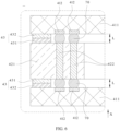
- FIG. 9 schematically shows a partial cross-sectional structure of the circuit board assembly 40 according to an embodiment of this application.
- the frame plate 42 further includes third pads 423.
- the third pads 423 are provided on the frame body 421.
- a material of the third pads 423 may be copper or a copper alloy.
- the third pads 423 are non-functional pads.
- the third pads 423 each are covered by the first support portion 431.
- An area of the first support portion 431 may be greater than an area of the third pad 423, and the entire third pad 423 is located below the first support portion 431.
- an area of the first support portion 431 may be equal to an area of the third pad 423, and the first support portion 431 is located on one side of the third pad 423.
- the first pad 422 and the third pad 423 are spaced apart.
- the third pads 423 can play a function of positioning references, to help quickly and accurately provide the first support portions 431 at predetermined locations of the frame body 421. This ensures that the first support portions 431 are located at the predetermined locations, reduces a possibility that support areas between the first support portions 431 and the second support portions 432 become smaller due to misalignment with the second support portions 432 that is resulted from deviation of the first support portions 431 from the predetermined locations, and is also conducive to reducing production difficulty and improving production efficiency.
- the circuit board 41 further includes fourth pads 413.
- the fourth pads 413 are provided on the board body 411.
- a material of the fourth pads 413 may be copper or a copper alloy.
- the fourth pads 413 are non-functional pads.
- the fourth pads 413 each are covered by the second support portion 432.
- An area of the second support portion 432 may be greater than an area of the fourth pad 413, and the entire fourth pad 413 is located below the second support portion 432.
- an area of the second support portion 432 may be equal to an area of the fourth pad 413, and the second support portion 432 is located on one side of the fourth pad 413.
- the third pads 423 and the fourth pads 413 are correspondingly provided.
- the fourth pads 413 can play a function of positioning references, to help quickly and accurately provide the second support portions 432 at predetermined locations of the board body 411. This ensures that the second support portions 432 are located at the predetermined locations, reduces a possibility that support areas between the first support portions 431 and the second support portions 432 become smaller due to misalignment with the first support portions 431 that is resulted from deviation of the second support portions 432 from the predetermined locations, and is also conducive to reducing production difficulty and improving production efficiency.
- a surface of the first pad 422 that faces the second pad 412 is flush with a surface of the third pad 423 that faces the fourth pad 413.
- a surface of the second pad 412 that faces the first pad 422 is flush with a surface of the fourth pad 413 that faces the third pad 423.
- the surface of the first pad 422 that faces the second pad 412, the surface of the third pad 423 that faces the fourth pad 413, the surface of the second pad 412 that faces the first pad 422, and the surface of the fourth pad 413 that faces the third pad 423 are all planar surfaces.
- FIG. 10 schematically shows a partial cross-sectional structure of the circuit board assembly 40 according to an embodiment of this application.
- the support body 43 further includes a third support portion 433 and a fourth support portion 434.
- the first support portion 431, the second support portion 432, the third support portion 433, and the fourth support portion 434 are stacked along the thickness direction X of the frame plate 42.
- the third support portion 433 is provided on a surface of the first support portion 431 that faces the second support portion 432.
- the fourth support portion 434 is provided on a surface of the second support portion 432 that faces the first support portion 431.
- the spacing between the first pads 422 and the second pads 412 can be further increased by using the third support portion 433 and the fourth support portion 434. Therefore, by controlling thicknesses of the third support portion 433 and the fourth support portion 434, the spacing between the first pads 422 and the second pads 412 can be adjusted to improve application flexibility of the support bodies 43, and the spacing between the first pads 422 and the second pads 412 can be accurately adjusted and controlled.
- the circuit board 41 When the circuit board 41 is connected to the frame plate 42, after the solder paste is printed on the first pads 422, the circuit board 41 is placed on one side of the frame plate 42, and the fourth support portion 434 on the board body 411 of the circuit board 41 is made corresponding to the third support portion 433 on the frame body 421, and the first pads 422 are made corresponding to the second pads 412.
- the third support portion 433 abuts against the fourth support portion 434, so that the support body 43 plays a supporting function.
- the spacing between the first pads 422 and the second pads 412 is equal to a sum of the thicknesses of the first support portion 431, the second support portion 432, the third support portion 433, and the fourth support portion 434.
- Both the third support portion 433 and the fourth support portion 434 are solder resist layers. Both the third support portion 433 and the fourth support portion 434 have good heat resistance. When the solder paste is heated and melted, the third support portion 433 and the fourth support portion 434 are not easily melted. This reduces a possibility that the circuit board 41 moves close to the frame plate 42 because the third support portion 433 and the fourth support portion 434 are melted and lose their support functions.
- the third support portion 433 and the fourth support portion 434 each are insulating materials.
- the third support portion 433 or the fourth support portion 434 does not electrically connect two first pads 422 or two second pads 412 and therefore does not cause a short circuit.
- both the third support portion 433 and the fourth support portion 434 are second solder resist ink layers.
- a material of the second solder resist ink layers is white ink.
- the second solder resist ink layer is printed on the first support portion 431, and the second solder resist ink layer forms the third support portion 433 with large hardness after being cured.
- the second solder resist ink layer is printed on the second support portion 432, and the second solder resist ink layer forms the fourth support portion 434 with large hardness after being cured.
- both the third support portion 433 and the fourth support portion 434 are insulating sheets.
- materials of the third support portion 433 and the fourth support portion 434 are both plastic, for example, polyethylene terephthalate, polyvinyl chloride, polyethylene, or polypropylene.
- a third support portion 433 and a fourth support portion 434 that have a predetermined length and width may be pre-processed and pre-manufactured by finish machining. Then, the third support portion 433 is provided on the first support portion 431, and the fourth support portion 434 is provided on the second support portion 432.
- the third support portion 433 may be attached to the first support portion 431, and the fourth support portion 434 may be attached to the second support portion 432.
- the third support portion 433 is at least partially located between the third pad 423 and the fourth pad 413.
- the fourth support portion 434 is at least partially located between the third pad 423 and the fourth pad 413.
- Both the third support portion 433 and the fourth support portion 434 are disc-shaped structures. Cross sections of the third pads 423 and the fourth pads 413 may be circular.
- a sum of the thicknesses of the first support portion 431 and the third support portion 433 is equal to a sum of the thicknesses of the second support portion 432 and the fourth support portion 434.
- the first support portion 431 and the second support portion 432 have a same thickness
- the third support portion 433 and the fourth support portion 434 have a same thickness.
- the thickness of the first support portion 431 is less than the thickness of the second support portion 432
- the thickness of the third support portion 433 is greater than the thickness of the fourth support portion 434.
- the thickness of the first support portion 431 is greater than the thickness of the second support portion 432
- the thickness of the third support portion 433 is less than the thickness of the fourth support portion 434.
- the third support portion 433 has a uniform thickness
- the fourth support portion 434 has a uniform thickness. This can facilitate printing of the second solder resist ink layer with the uniform thickness on the frame body 421 or the board body 411 by using a printing process to form the third support portion 433 or the fourth support portion 434, thereby reducing difficulty in manufacturing the third support portion 433 and the fourth support portion 434.
- insulating sheets with a predetermined thickness are pre-processed and pre-manufactured by finish machining.
- the thickness of the third support portion 433 is equal to the thickness of the fourth support portion 434. This facilitates printing and forming of the second solder resist ink layer on the frame body 421 or the board body 411 by using a printed board with a same thickness, or insulating sheets with a predetermined thickness can be pre-processed and pre-manufactured by finish machining, thereby reducing a possibility of complex processing operations and high production costs caused by a need of processing insulating sheets with two different thicknesses to form the third support portion 433 and the fourth support portion 434.
- connection may be a fixed connection, an indirect connection through an intermediate medium, internal communication between two elements, or an interaction relationship between two elements.
- connection may be a fixed connection, an indirect connection through an intermediate medium, internal communication between two elements, or an interaction relationship between two elements.
- a plurality of in this specification refers to two or more.
- the term “and/or” in this specification describes only an association relationship for describing associated objects and represents that three relationships can exist. For example, “A and/or B” can represent the following three cases: Only A exists, both A and B exist, and only B exists.
- the character “/” in this specification generally indicates an "or” relationship between the associated objects. In a formula, the character “/” indicates that the associated objects are in a "division" relationship.
- sequence number of each of the foregoing processes does not mean a sequence of execution.
- the sequence of execution of the processes should be determined based on functions and internal logic of the processes, and no limitation should be imposed on an implementation process of the embodiments of this application.
Landscapes
- Engineering & Computer Science (AREA)
- Microelectronics & Electronic Packaging (AREA)
- Manufacturing & Machinery (AREA)
- Combinations Of Printed Boards (AREA)
- Mounting Of Printed Circuit Boards And The Like (AREA)
- Structure Of Printed Boards (AREA)
Claims (15)
- Eine Leiterplattenbaugruppe (40) zur Verwendung in einem elektronischen Gerät (10), umfassend mindestens Folgendes:eine Rahmenplatte (42), umfassend einen Rahmenkörper (421) und erste Pads (422), wobei die ersten Pads auf dem Rahmenkörper vorgesehen sind;Leiterplatten (41), die jeweils auf einer Seite der Rahmenplatte vorgesehen sind, wobei die Leiterplatte einen Plattenkörper (411) und zweite Pads (412) umfasst, die zweiten Pads auf dem Plattenkörper vorgesehen sind und die ersten Pads den zweiten Pads gegenüberliegen;Stützkörper (43), die zwischen der Rahmenplatte und den Leiterplatten vorgesehen sind, wobei die Stützkörper so konfiguriert sind, dass sie die Leiterplatten stützen, sodass ein vorgegebener Abstand (L) zwischen den ersten Pads und den zweiten Pads besteht, die Stützkörper umfassen jeweils einen ersten Stützabschnitt (431) und einen zweiten Stützabschnitt (432), der erste Stützabschnitt und der zweite Stützabschnitt sind entlang einer Dicke (X) der Rahmenplatte gestapelt, der erste Stützabschnitt ist mit dem Rahmenkörper verbunden, und der zweite Stützabschnitt ist mit dem Plattenkörper verbunden; undLötverbindungen (70), die zwischen den ersten Pads und den zweiten Pads vorgesehen sind, wobei die Lötverbindungen die ersten Pads mit den zweiten Pads verbinden, wobei der Rahmenkörper eine ringförmige Struktur ist und zwei oder mehr Stützkörper entlang einer Umfangsrichtung des Rahmenkörpers beabstandet sind.
- Die Leiterplattenbaugruppe nach Anspruch 1, wobei zwei oder mehr Stützkörper gleichmäßig entlang der Umfangsrichtung des Rahmenkörpers verteilt sind.
- Die Leiterplattenbaugruppe nach einem der Ansprüche 1 bis 2, wobei sowohl der erste Stützabschnitt als auch der zweite Stützabschnitt Lötstopp-Schichten sind.
- Die Leiterplattenbaugruppe nach Anspruch 3, wobei sowohl der erste Stützabschnitt als auch der zweite Stützabschnitt erste Lötstopp-Tintenschichten sind.
- Die Leiterplattenbaugruppe nach einem der Ansprüche 1 bis 4, wobei der erste Stützabschnitt eine einheitliche Dicke aufweist und der zweite Stützabschnitt eine einheitliche Dicke aufweist.
- Die Leiterplattenbaugruppe nach Anspruch 5, wobei die Dicke des ersten Stützabschnitts gleich der Dicke des zweiten Stützabschnitts ist.
- Die Leiterplattenbaugruppe nach einem der Ansprüche 1 bis 6, wobei der Stützkörper ferner einen dritten Stützabschnitt (433) und einen vierten Stützabschnitt (434) umfasst, der erste Stützabschnitt, der zweite Stützabschnitt, der dritte Stützabschnitt und der vierte Stützabschnitt gestapelt sind, der dritte Stützabschnitt auf einer Oberfläche des ersten Stützabschnitts vorgesehen ist, die dem zweiten Stützabschnitt zugewandt ist, und der vierte Stützabschnitt auf einer Oberfläche des zweiten Stützabschnitts vorgesehen ist, die dem ersten Stützabschnitt zugewandt ist.
- Die Leiterplattenbaugruppe gemäß Anspruch 7, wobei sowohl der dritte Stützabschnitt als auch der vierte Stützabschnitt Lötstoppmaskenschichten sind.
- Die Leiterplattenbaugruppe gemäß Anspruch 8, wobei sowohl der dritte Stützabschnitt als auch der vierte Stützabschnitt zweite Lötstoppmaskenfarbschichten sind; oder sowohl der dritte Stützabschnitt als auch der vierte Stützabschnitt Isolierfolien sind.
- Die Leiterplattenbaugruppe gemäß einem der Ansprüche 7 bis 9, wobei die Summe der Dicken des ersten Stützabschnitts und des dritten Stützabschnitts gleich der Summe der Dicken des zweiten Stützabschnitts und des vierten Stützabschnitts ist.
- Die Leiterplattenbaugruppe gemäß Anspruch 10, wobei der dritte Stützabschnitt eine einheitliche Dicke aufweist und der vierte Stützabschnitt eine einheitliche Dicke aufweist.
- Die Leiterplattenbaugruppe gemäß Anspruch 11, wobei die Dicke des dritten Stützabschnitts gleich der Dicke des vierten Stützabschnitts ist.
- Die Leiterplattenbaugruppe gemäß Anspruch 1, wobei die Rahmenplatte ferner dritte Pads (423) umfasst, die dritten Pads am Rahmenkörper vorgesehen sind, die dritten Pads jeweils vom ersten Stützabschnitt bedeckt sind, und die Leiterplatte ferner vierte Pads (413) umfasst, die dritten Pads den vierten Pads gegenüberliegen, und die vierten Pads jeweils vom zweiten Stützabschnitt bedeckt sind.
- Die Leiterplattenbaugruppe gemäß Anspruch 13, wobei eine Oberfläche des ersten Pads, die dem zweiten Pad zugewandt ist, bündig mit einer Oberfläche des dritten Pads ist, die dem vierten Pad zugewandt ist, und eine Oberfläche des zweiten Pads, die dem ersten Pad zugewandt ist, bündig mit einer Oberfläche des vierten Pads ist, die dem dritten Pad zugewandt ist.
- Ein elektronisches Gerät (10), umfassend die Leiterplattenbaugruppe gemäß einem der Ansprüche 1 bis 14.
Priority Applications (1)
| Application Number | Priority Date | Filing Date | Title |
|---|---|---|---|
| EP25166570.9A EP4626153A3 (de) | 2021-09-18 | 2022-08-18 | Leiterplattenanordnung und elektronische vorrichtung |
Applications Claiming Priority (2)
| Application Number | Priority Date | Filing Date | Title |
|---|---|---|---|
| CN202111113468.8A CN115023033B (zh) | 2021-09-18 | 2021-09-18 | 电路板组件以及电子设备 |
| PCT/CN2022/113347 WO2023040572A1 (zh) | 2021-09-18 | 2022-08-18 | 电路板组件以及电子设备 |
Related Child Applications (1)
| Application Number | Title | Priority Date | Filing Date |
|---|---|---|---|
| EP25166570.9A Division EP4626153A3 (de) | 2021-09-18 | 2022-08-18 | Leiterplattenanordnung und elektronische vorrichtung |
Publications (3)
| Publication Number | Publication Date |
|---|---|
| EP4192206A1 EP4192206A1 (de) | 2023-06-07 |
| EP4192206A4 EP4192206A4 (de) | 2024-07-03 |
| EP4192206B1 true EP4192206B1 (de) | 2025-04-23 |
Family
ID=83065191
Family Applications (2)
| Application Number | Title | Priority Date | Filing Date |
|---|---|---|---|
| EP25166570.9A Pending EP4626153A3 (de) | 2021-09-18 | 2022-08-18 | Leiterplattenanordnung und elektronische vorrichtung |
| EP22859527.8A Active EP4192206B1 (de) | 2021-09-18 | 2022-08-18 | Leiterplattenanordnung und elektronische vorrichtung |
Family Applications Before (1)
| Application Number | Title | Priority Date | Filing Date |
|---|---|---|---|
| EP25166570.9A Pending EP4626153A3 (de) | 2021-09-18 | 2022-08-18 | Leiterplattenanordnung und elektronische vorrichtung |
Country Status (4)
| Country | Link |
|---|---|
| US (1) | US12219727B2 (de) |
| EP (2) | EP4626153A3 (de) |
| CN (3) | CN115023033B (de) |
| WO (1) | WO2023040572A1 (de) |
Families Citing this family (3)
| Publication number | Priority date | Publication date | Assignee | Title |
|---|---|---|---|---|
| CN115023033B (zh) * | 2021-09-18 | 2023-06-06 | 荣耀终端有限公司 | 电路板组件以及电子设备 |
| CN116744548B (zh) * | 2022-09-20 | 2024-05-10 | 荣耀终端有限公司 | 电路板组件及其加工方法、电子设备 |
| CN116761335A (zh) * | 2023-07-12 | 2023-09-15 | 深圳盛凌电子股份有限公司 | 芯片电子装置及其装配方法 |
Family Cites Families (31)
| Publication number | Priority date | Publication date | Assignee | Title |
|---|---|---|---|---|
| GB8727926D0 (en) * | 1987-11-28 | 1987-12-31 | British Aerospace | Surface mounting leadless components on conductor pattern supporting substrates |
| JP2003068920A (ja) * | 2001-08-27 | 2003-03-07 | Kyocera Corp | 配線基板 |
| US7201583B2 (en) * | 2003-12-31 | 2007-04-10 | Intel Corporation | Three-dimensional flexible interposer |
| US7521847B2 (en) * | 2005-03-21 | 2009-04-21 | Artificial Muscle, Inc. | High-performance electroactive polymer transducers |
| JP4232834B2 (ja) * | 2007-03-07 | 2009-03-04 | セイコーエプソン株式会社 | アクチュエータ、光スキャナおよび画像形成装置 |
| JP2009099367A (ja) * | 2007-10-16 | 2009-05-07 | Fuji Heavy Ind Ltd | 発光装置 |
| CN104113983A (zh) * | 2013-04-17 | 2014-10-22 | 深南电路有限公司 | 一种埋入式电路板及其制作方法 |
| US9204543B2 (en) * | 2013-12-03 | 2015-12-01 | Infineon Technologies Ag | Integrated IC package |
| US9560742B2 (en) * | 2014-11-11 | 2017-01-31 | Alcatel Lucent | Backdrill reliability anchors |
| CN105491818B (zh) * | 2015-11-23 | 2018-12-28 | 广州兴森快捷电路科技有限公司 | 高对位精度的埋线路板制作方法 |
| CN108235832B (zh) * | 2017-03-09 | 2021-01-05 | 华为技术有限公司 | 一种消费电子产品的主板及终端 |
| CN207720522U (zh) | 2017-12-08 | 2018-08-10 | 东莞市久源隆电路板有限公司 | 一种层叠布置的电路板 |
| WO2019130978A1 (ja) * | 2017-12-28 | 2019-07-04 | 株式会社村田製作所 | 基板接合構造 |
| KR102505441B1 (ko) | 2018-02-19 | 2023-03-03 | 삼성전기주식회사 | 인쇄회로기판 및 이를 구비한 전자기기 |
| CN210008007U (zh) * | 2019-03-28 | 2020-01-31 | 联想(北京)有限公司 | 电子设备 |
| KR102827056B1 (ko) | 2019-04-16 | 2025-07-01 | 엘지이노텍 주식회사 | 플렉서블 회로기판 및 이를 포함하는 플렉서블 장치 |
| CN110337178B (zh) * | 2019-04-25 | 2021-03-23 | 维沃移动通信有限公司 | 一种电路板组件和电子设备 |
| CN110191579B (zh) * | 2019-06-11 | 2020-12-08 | Oppo广东移动通信有限公司 | 电路板组件及电子设备 |
| CN112243314A (zh) * | 2019-07-18 | 2021-01-19 | 华为技术有限公司 | 一种电路板组件、电路板组件的制作方法及电子设备 |
| CN112437979A (zh) * | 2019-07-24 | 2021-03-02 | 深圳市大疆创新科技有限公司 | 电子封装组件、相机、可移动平台及其制备方法 |
| CN110519919B (zh) * | 2019-09-05 | 2021-07-13 | 维沃移动通信有限公司 | 框架式转接板及其制备方法、电路板装置及电子设备 |
| CN210670769U (zh) * | 2019-10-29 | 2020-06-02 | 维沃移动通信有限公司 | 一种电路板组件及电子设备 |
| CN111010798B (zh) | 2019-12-31 | 2021-05-11 | 华为技术有限公司 | 电路板及电子装置 |
| CN211210039U (zh) * | 2020-02-20 | 2020-08-07 | 维沃移动通信有限公司 | 一种电路板结构及电子设备 |
| CN212677451U (zh) * | 2020-04-20 | 2021-03-09 | 华为技术有限公司 | 一种装配印刷电路板及电子设备 |
| CN111698827A (zh) * | 2020-04-27 | 2020-09-22 | 华为技术有限公司 | 电路板组件、电子设备、电路板组件的加工方法 |
| CN212324455U (zh) | 2020-06-11 | 2021-01-08 | 维沃移动通信有限公司 | 电路板、电路板组件以及电子设备 |
| CN212463649U (zh) * | 2020-07-30 | 2021-02-02 | 维沃移动通信有限公司 | 电路板装置及电子设备 |
| CN213073214U (zh) * | 2020-09-22 | 2021-04-27 | 深圳市大疆创新科技有限公司 | 转接电路板和堆叠电路板 |
| CN213694596U (zh) | 2020-12-17 | 2021-07-13 | 维沃移动通信有限公司 | 电路板结构及电子设备 |
| CN115023033B (zh) | 2021-09-18 | 2023-06-06 | 荣耀终端有限公司 | 电路板组件以及电子设备 |
-
2021
- 2021-09-18 CN CN202111113468.8A patent/CN115023033B/zh active Active
-
2022
- 2022-08-18 CN CN202280007617.9A patent/CN116602062B8/zh active Active
- 2022-08-18 WO PCT/CN2022/113347 patent/WO2023040572A1/zh not_active Ceased
- 2022-08-18 US US18/025,470 patent/US12219727B2/en active Active
- 2022-08-18 EP EP25166570.9A patent/EP4626153A3/de active Pending
- 2022-08-18 EP EP22859527.8A patent/EP4192206B1/de active Active
- 2022-08-18 CN CN202410311178.1A patent/CN118400873A/zh active Pending
Also Published As
| Publication number | Publication date |
|---|---|
| CN116602062B8 (zh) | 2024-06-04 |
| CN115023033B (zh) | 2023-06-06 |
| US20240206102A1 (en) | 2024-06-20 |
| CN116602062B (zh) | 2024-03-26 |
| EP4192206A4 (de) | 2024-07-03 |
| WO2023040572A1 (zh) | 2023-03-23 |
| EP4192206A1 (de) | 2023-06-07 |
| CN118400873A (zh) | 2024-07-26 |
| EP4626153A3 (de) | 2025-12-10 |
| CN116602062A (zh) | 2023-08-15 |
| CN115023033A (zh) | 2022-09-06 |
| EP4626153A2 (de) | 2025-10-01 |
| US12219727B2 (en) | 2025-02-04 |
Similar Documents
| Publication | Publication Date | Title |
|---|---|---|
| EP4626153A2 (de) | Leiterplattenanordnung und elektronische vorrichtung | |
| EP4178325B1 (de) | Leiterplattenanordnung und elektronische vorrichtung | |
| CN115023037B (zh) | 电路板组件以及电子设备 | |
| CN108235832A (zh) | 一种消费电子产品的主板及终端 | |
| EP4194132B1 (de) | Leiterplattenanordnungsschweissvorrichtung und leiterplattenanordnungsschweissverfahren | |
| JP4353181B2 (ja) | 電子装置の製造方法 | |
| EP4175424A1 (de) | Leiterplattenanordnung und elektronische vorrichtung | |
| CN101460020A (zh) | 多层柔性电路板 | |
| CN115038284B (zh) | 电路板组件以及电子设备 | |
| HK40077640B (en) | Circuit board assembly and electronic device | |
| HK40077640A (en) | Circuit board assembly and electronic device | |
| US9241406B2 (en) | Electronic assembly | |
| US20240306300A1 (en) | Flexible Circuit Board, Circuit Board Assembly, and Electronic Device | |
| US10231342B2 (en) | Component built-in substrate | |
| CN116801484B (zh) | 一种单板及其制备方法、电子设备 | |
| CN217607013U (zh) | 一种栅格阵列封装天线和电子设备 | |
| CN217849777U (zh) | 主板组件和电子设备 | |
| CN219644197U (zh) | 电池保护板、锂电池以及电子设备 | |
| CN217088249U (zh) | 转接板、叠板结构及电子设备 | |
| CN210551594U (zh) | 一种平衡模冲拉力的定位结构 | |
| CN105636352A (zh) | 硬板及具有其的移动终端 | |
| HK40077917B (en) | Circuit board component and electronic device |
Legal Events
| Date | Code | Title | Description |
|---|---|---|---|
| STAA | Information on the status of an ep patent application or granted ep patent |
Free format text: STATUS: UNKNOWN |
|
| STAA | Information on the status of an ep patent application or granted ep patent |
Free format text: STATUS: THE INTERNATIONAL PUBLICATION HAS BEEN MADE |
|
| PUAI | Public reference made under article 153(3) epc to a published international application that has entered the european phase |
Free format text: ORIGINAL CODE: 0009012 |
|
| STAA | Information on the status of an ep patent application or granted ep patent |
Free format text: STATUS: REQUEST FOR EXAMINATION WAS MADE |
|
| 17P | Request for examination filed |
Effective date: 20230301 |
|
| AK | Designated contracting states |
Kind code of ref document: A1 Designated state(s): AL AT BE BG CH CY CZ DE DK EE ES FI FR GB GR HR HU IE IS IT LI LT LU LV MC MK MT NL NO PL PT RO RS SE SI SK SM TR |
|
| REG | Reference to a national code |
Ref legal event code: R079 Ipc: H05K0001140000 Ref country code: DE Ref legal event code: R079 Ref document number: 602022013704 Country of ref document: DE Free format text: PREVIOUS MAIN CLASS: H05K0001110000 Ipc: H05K0001140000 |
|
| A4 | Supplementary search report drawn up and despatched |
Effective date: 20240603 |
|
| RIC1 | Information provided on ipc code assigned before grant |
Ipc: H05K 1/11 20060101ALN20240527BHEP Ipc: H05K 3/36 20060101ALI20240527BHEP Ipc: H05K 3/34 20060101ALI20240527BHEP Ipc: H05K 1/14 20060101AFI20240527BHEP |
|
| GRAP | Despatch of communication of intention to grant a patent |
Free format text: ORIGINAL CODE: EPIDOSNIGR1 |
|
| STAA | Information on the status of an ep patent application or granted ep patent |
Free format text: STATUS: GRANT OF PATENT IS INTENDED |
|
| RIC1 | Information provided on ipc code assigned before grant |
Ipc: H05K 1/11 20060101ALN20241107BHEP Ipc: H05K 3/36 20060101ALI20241107BHEP Ipc: H05K 3/34 20060101ALI20241107BHEP Ipc: H05K 1/14 20060101AFI20241107BHEP |
|
| INTG | Intention to grant announced |
Effective date: 20241118 |
|
| RIC1 | Information provided on ipc code assigned before grant |
Ipc: H05K 1/11 20060101ALN20241111BHEP Ipc: H05K 3/36 20060101ALI20241111BHEP Ipc: H05K 3/34 20060101ALI20241111BHEP Ipc: H05K 1/14 20060101AFI20241111BHEP |
|
| DAV | Request for validation of the european patent (deleted) | ||
| DAX | Request for extension of the european patent (deleted) | ||
| GRAS | Grant fee paid |
Free format text: ORIGINAL CODE: EPIDOSNIGR3 |
|
| GRAA | (expected) grant |
Free format text: ORIGINAL CODE: 0009210 |
|
| STAA | Information on the status of an ep patent application or granted ep patent |
Free format text: STATUS: THE PATENT HAS BEEN GRANTED |
|
| AK | Designated contracting states |
Kind code of ref document: B1 Designated state(s): AL AT BE BG CH CY CZ DE DK EE ES FI FR GB GR HR HU IE IS IT LI LT LU LV MC MK MT NL NO PL PT RO RS SE SI SK SM TR |
|
| REG | Reference to a national code |
Ref country code: GB Ref legal event code: FG4D |
|
| REG | Reference to a national code |
Ref country code: CH Ref legal event code: EP |
|
| REG | Reference to a national code |
Ref country code: DE Ref legal event code: R096 Ref document number: 602022013704 Country of ref document: DE |
|
| REG | Reference to a national code |
Ref country code: IE Ref legal event code: FG4D |
|
| REG | Reference to a national code |
Ref country code: NL Ref legal event code: FP |
|
| PGFP | Annual fee paid to national office [announced via postgrant information from national office to epo] |
Ref country code: NL Payment date: 20250704 Year of fee payment: 4 |
|
| REG | Reference to a national code |
Ref country code: AT Ref legal event code: MK05 Ref document number: 1789098 Country of ref document: AT Kind code of ref document: T Effective date: 20250423 |
|
| PG25 | Lapsed in a contracting state [announced via postgrant information from national office to epo] |
Ref country code: FI Free format text: LAPSE BECAUSE OF FAILURE TO SUBMIT A TRANSLATION OF THE DESCRIPTION OR TO PAY THE FEE WITHIN THE PRESCRIBED TIME-LIMIT Effective date: 20250423 Ref country code: ES Free format text: LAPSE BECAUSE OF FAILURE TO SUBMIT A TRANSLATION OF THE DESCRIPTION OR TO PAY THE FEE WITHIN THE PRESCRIBED TIME-LIMIT Effective date: 20250423 Ref country code: PT Free format text: LAPSE BECAUSE OF FAILURE TO SUBMIT A TRANSLATION OF THE DESCRIPTION OR TO PAY THE FEE WITHIN THE PRESCRIBED TIME-LIMIT Effective date: 20250825 |
|
| PGFP | Annual fee paid to national office [announced via postgrant information from national office to epo] |
Ref country code: DE Payment date: 20250702 Year of fee payment: 4 |
|
| REG | Reference to a national code |
Ref country code: LT Ref legal event code: MG9D |
|
| PG25 | Lapsed in a contracting state [announced via postgrant information from national office to epo] |
Ref country code: NO Free format text: LAPSE BECAUSE OF FAILURE TO SUBMIT A TRANSLATION OF THE DESCRIPTION OR TO PAY THE FEE WITHIN THE PRESCRIBED TIME-LIMIT Effective date: 20250723 Ref country code: GR Free format text: LAPSE BECAUSE OF FAILURE TO SUBMIT A TRANSLATION OF THE DESCRIPTION OR TO PAY THE FEE WITHIN THE PRESCRIBED TIME-LIMIT Effective date: 20250724 |
|
| PG25 | Lapsed in a contracting state [announced via postgrant information from national office to epo] |
Ref country code: PL Free format text: LAPSE BECAUSE OF FAILURE TO SUBMIT A TRANSLATION OF THE DESCRIPTION OR TO PAY THE FEE WITHIN THE PRESCRIBED TIME-LIMIT Effective date: 20250423 |
|
| PG25 | Lapsed in a contracting state [announced via postgrant information from national office to epo] |
Ref country code: BG Free format text: LAPSE BECAUSE OF FAILURE TO SUBMIT A TRANSLATION OF THE DESCRIPTION OR TO PAY THE FEE WITHIN THE PRESCRIBED TIME-LIMIT Effective date: 20250423 |
|
| PG25 | Lapsed in a contracting state [announced via postgrant information from national office to epo] |
Ref country code: HR Free format text: LAPSE BECAUSE OF FAILURE TO SUBMIT A TRANSLATION OF THE DESCRIPTION OR TO PAY THE FEE WITHIN THE PRESCRIBED TIME-LIMIT Effective date: 20250423 |
|
| PG25 | Lapsed in a contracting state [announced via postgrant information from national office to epo] |
Ref country code: AT Free format text: LAPSE BECAUSE OF FAILURE TO SUBMIT A TRANSLATION OF THE DESCRIPTION OR TO PAY THE FEE WITHIN THE PRESCRIBED TIME-LIMIT Effective date: 20250423 |
|
| PG25 | Lapsed in a contracting state [announced via postgrant information from national office to epo] |
Ref country code: RS Free format text: LAPSE BECAUSE OF FAILURE TO SUBMIT A TRANSLATION OF THE DESCRIPTION OR TO PAY THE FEE WITHIN THE PRESCRIBED TIME-LIMIT Effective date: 20250723 |
|
| PG25 | Lapsed in a contracting state [announced via postgrant information from national office to epo] |
Ref country code: IS Free format text: LAPSE BECAUSE OF FAILURE TO SUBMIT A TRANSLATION OF THE DESCRIPTION OR TO PAY THE FEE WITHIN THE PRESCRIBED TIME-LIMIT Effective date: 20250823 |
|
| PG25 | Lapsed in a contracting state [announced via postgrant information from national office to epo] |
Ref country code: LV Free format text: LAPSE BECAUSE OF FAILURE TO SUBMIT A TRANSLATION OF THE DESCRIPTION OR TO PAY THE FEE WITHIN THE PRESCRIBED TIME-LIMIT Effective date: 20250423 |
|
| PG25 | Lapsed in a contracting state [announced via postgrant information from national office to epo] |
Ref country code: SM Free format text: LAPSE BECAUSE OF FAILURE TO SUBMIT A TRANSLATION OF THE DESCRIPTION OR TO PAY THE FEE WITHIN THE PRESCRIBED TIME-LIMIT Effective date: 20250423 Ref country code: DK Free format text: LAPSE BECAUSE OF FAILURE TO SUBMIT A TRANSLATION OF THE DESCRIPTION OR TO PAY THE FEE WITHIN THE PRESCRIBED TIME-LIMIT Effective date: 20250423 |
|
| PG25 | Lapsed in a contracting state [announced via postgrant information from national office to epo] |
Ref country code: CZ Free format text: LAPSE BECAUSE OF FAILURE TO SUBMIT A TRANSLATION OF THE DESCRIPTION OR TO PAY THE FEE WITHIN THE PRESCRIBED TIME-LIMIT Effective date: 20250423 |
|
| PG25 | Lapsed in a contracting state [announced via postgrant information from national office to epo] |
Ref country code: EE Free format text: LAPSE BECAUSE OF FAILURE TO SUBMIT A TRANSLATION OF THE DESCRIPTION OR TO PAY THE FEE WITHIN THE PRESCRIBED TIME-LIMIT Effective date: 20250423 |
|
| REG | Reference to a national code |
Ref country code: DE Ref legal event code: R097 Ref document number: 602022013704 Country of ref document: DE |
|
| PG25 | Lapsed in a contracting state [announced via postgrant information from national office to epo] |
Ref country code: SK Free format text: LAPSE BECAUSE OF FAILURE TO SUBMIT A TRANSLATION OF THE DESCRIPTION OR TO PAY THE FEE WITHIN THE PRESCRIBED TIME-LIMIT Effective date: 20250423 |
|
| PG25 | Lapsed in a contracting state [announced via postgrant information from national office to epo] |
Ref country code: IT Free format text: LAPSE BECAUSE OF FAILURE TO SUBMIT A TRANSLATION OF THE DESCRIPTION OR TO PAY THE FEE WITHIN THE PRESCRIBED TIME-LIMIT Effective date: 20250423 |
|
| PLBE | No opposition filed within time limit |
Free format text: ORIGINAL CODE: 0009261 |
|
| STAA | Information on the status of an ep patent application or granted ep patent |
Free format text: STATUS: NO OPPOSITION FILED WITHIN TIME LIMIT |
|
| REG | Reference to a national code |
Ref country code: CH Ref legal event code: L10 Free format text: ST27 STATUS EVENT CODE: U-0-0-L10-L00 (AS PROVIDED BY THE NATIONAL OFFICE) Effective date: 20260304 |
|
| PG25 | Lapsed in a contracting state [announced via postgrant information from national office to epo] |
Ref country code: RO Free format text: LAPSE BECAUSE OF FAILURE TO SUBMIT A TRANSLATION OF THE DESCRIPTION OR TO PAY THE FEE WITHIN THE PRESCRIBED TIME-LIMIT Effective date: 20250423 |
|
| REG | Reference to a national code |
Ref country code: CH Ref legal event code: H13 Free format text: ST27 STATUS EVENT CODE: U-0-0-H10-H13 (AS PROVIDED BY THE NATIONAL OFFICE) Effective date: 20260324 |
|
| PG25 | Lapsed in a contracting state [announced via postgrant information from national office to epo] |
Ref country code: MC Free format text: LAPSE BECAUSE OF FAILURE TO SUBMIT A TRANSLATION OF THE DESCRIPTION OR TO PAY THE FEE WITHIN THE PRESCRIBED TIME-LIMIT Effective date: 20250423 |
|
| 26N | No opposition filed |
Effective date: 20260126 |
|
| PG25 | Lapsed in a contracting state [announced via postgrant information from national office to epo] |
Ref country code: LU Free format text: LAPSE BECAUSE OF NON-PAYMENT OF DUE FEES Effective date: 20250818 |
|
| PG25 | Lapsed in a contracting state [announced via postgrant information from national office to epo] |
Ref country code: CH Free format text: LAPSE BECAUSE OF NON-PAYMENT OF DUE FEES Effective date: 20250831 |