EP4186428B1 - Strahlungsabbildungsvorrichtung - Google Patents
Strahlungsabbildungsvorrichtung Download PDFInfo
- Publication number
- EP4186428B1 EP4186428B1 EP22205391.0A EP22205391A EP4186428B1 EP 4186428 B1 EP4186428 B1 EP 4186428B1 EP 22205391 A EP22205391 A EP 22205391A EP 4186428 B1 EP4186428 B1 EP 4186428B1
- Authority
- EP
- European Patent Office
- Prior art keywords
- radiation
- pixels
- detection
- pixel
- grid
- Prior art date
- Legal status (The legal status is an assumption and is not a legal conclusion. Google has not performed a legal analysis and makes no representation as to the accuracy of the status listed.)
- Active
Links
Images


Classifications
-
- A—HUMAN NECESSITIES
- A61—MEDICAL OR VETERINARY SCIENCE; HYGIENE
- A61B—DIAGNOSIS; SURGERY; IDENTIFICATION
- A61B6/00—Apparatus or devices for radiation diagnosis; Apparatus or devices for radiation diagnosis combined with radiation therapy equipment
- A61B6/42—Arrangements for detecting radiation specially adapted for radiation diagnosis
- A61B6/4208—Arrangements for detecting radiation specially adapted for radiation diagnosis characterised by using a particular type of detector
- A61B6/4233—Arrangements for detecting radiation specially adapted for radiation diagnosis characterised by using a particular type of detector using matrix detectors
-
- A—HUMAN NECESSITIES
- A61—MEDICAL OR VETERINARY SCIENCE; HYGIENE
- A61B—DIAGNOSIS; SURGERY; IDENTIFICATION
- A61B6/00—Apparatus or devices for radiation diagnosis; Apparatus or devices for radiation diagnosis combined with radiation therapy equipment
- A61B6/40—Arrangements for generating radiation specially adapted for radiation diagnosis
- A61B6/4035—Arrangements for generating radiation specially adapted for radiation diagnosis the source being combined with a filter or grating
-
- A—HUMAN NECESSITIES
- A61—MEDICAL OR VETERINARY SCIENCE; HYGIENE
- A61B—DIAGNOSIS; SURGERY; IDENTIFICATION
- A61B6/00—Apparatus or devices for radiation diagnosis; Apparatus or devices for radiation diagnosis combined with radiation therapy equipment
- A61B6/42—Arrangements for detecting radiation specially adapted for radiation diagnosis
- A61B6/4266—Arrangements for detecting radiation specially adapted for radiation diagnosis characterised by using a plurality of detector units
-
- A—HUMAN NECESSITIES
- A61—MEDICAL OR VETERINARY SCIENCE; HYGIENE
- A61B—DIAGNOSIS; SURGERY; IDENTIFICATION
- A61B6/00—Apparatus or devices for radiation diagnosis; Apparatus or devices for radiation diagnosis combined with radiation therapy equipment
- A61B6/42—Arrangements for detecting radiation specially adapted for radiation diagnosis
- A61B6/4291—Arrangements for detecting radiation specially adapted for radiation diagnosis the detector being combined with a grid or grating
-
- A—HUMAN NECESSITIES
- A61—MEDICAL OR VETERINARY SCIENCE; HYGIENE
- A61B—DIAGNOSIS; SURGERY; IDENTIFICATION
- A61B6/00—Apparatus or devices for radiation diagnosis; Apparatus or devices for radiation diagnosis combined with radiation therapy equipment
- A61B6/46—Arrangements for interfacing with the operator or the patient
- A61B6/461—Displaying means of special interest
-
- A—HUMAN NECESSITIES
- A61—MEDICAL OR VETERINARY SCIENCE; HYGIENE
- A61B—DIAGNOSIS; SURGERY; IDENTIFICATION
- A61B6/00—Apparatus or devices for radiation diagnosis; Apparatus or devices for radiation diagnosis combined with radiation therapy equipment
- A61B6/54—Control of apparatus or devices for radiation diagnosis
- A61B6/542—Control of apparatus or devices for radiation diagnosis involving control of exposure
Definitions
- the present invention relates to a radiation imaging apparatus and a radiation imaging system.
- Radiation imaging apparatuses having an automatic exposure control (AEC) function are known. Such a radiation imaging apparatus can measure a dose of radiation during emission, and based on a result of the measurement, the emission of radiation is terminated. For example, the radiation imaging apparatus monitors a dose of radiation by operating only pixels set for radiation detection at high speed during the emission of radiation.
- AEC automatic exposure control
- the grid has a structure in which an X-ray transmissive layer and an X-ray absorption layer each having a strip shape are alternately arranged, and the grid is disposed between the object and the imaging apparatus during image capturing.
- Japanese Patent No. 5969950 discusses a radiation imaging apparatus in which periodicity in the arrangement of dose detection sensors and periodicity in the arrangement of radiation absorption portions of a grid are different from each other. This configuration is to suppress a disproportionate influence on the dose detection sensors due to dose attenuation by the grid even in a case where the positional relationship between the dose detection sensors and the grid changes. In the technique of Japanese Patent No. 5969950 , however, there may be room for an improvement in the configuration to further decrease the disproportionate influence on the dose detection sensors due to the dose attenuation by the grid.
- the present invention is directed to providing a technology for improving the accuracy of automatic exposure control, by reducing or suppressing a disproportionate influence on signals of a plurality of radiation detection pixels in a region of interest due to attenuation by an X-ray absorption layer of a grid.
- Fig. 1 illustrates an example of a configuration of a radiation imaging apparatus 100 capable of performing radiography using a grid, according to a first exemplary embodiment of the present invention.
- the radiation imaging apparatus 100 has a plurality of pixels, which is arranged in an imaging region IR in a form of a plurality of rows and a plurality of columns, a plurality of driving lines 110, and a plurality of signal lines 120.
- the plurality of driving lines 110 is disposed to correspond to the plurality of rows of pixels, and each of the driving lines 110 corresponds to a different one of the pixel rows.
- the plurality of signal lines 120 is disposed to correspond to a plurality of columns of pixels, and each of the signal lines 120 corresponds to a different one of the pixel columns.
- the plurality of pixels includes a plurality of imaging pixels 101, which is used to acquire a radiation image, and one or more detection pixels 104 (hereinafter may also be referred to as the radiation detection pixels 104), which is used to monitor a dose of radiation, and a pixel unit is formed of the imaging pixels 101 and the detection pixels 104.
- the imaging pixel 101 includes a conversion element 102 for converting radiation into an electrical signal and a switch element 103 for connecting the corresponding signal line 120 and the conversion element 102.
- the detection pixel 104 includes a conversion element 105 for converting radiation into an electrical signal and a switch element 106 for connecting the corresponding signal line 120 and the conversion element 105.
- the detection pixel 104 is disposed in a row and a column formed of the plurality of imaging pixels 101. In Fig. 1 and subsequent figures, the conversion element 102 is not hatched and the conversion element 105 is hatched so as to be distinguishable between the imaging pixel 101 and the detection pixel 104.
- the conversion element 102 and the conversion element 105 can each be composed of a scintillator for converting radiation into light and a photoelectric conversion element for converting the light into an electrical signal.
- the scintillator is formed in a sheet form covering the imaging region IR and shared by a plurality of pixels.
- the conversion element 102 and the conversion element 105 can each be configured of a conversion element that directly converts radiation into an electrical signal.
- the switch element 103 and the switch element 106 can each include a thin-film transistor (TFT) in which an active region is formed of a semiconductor, such as an amorphous silicon or a polycrystalline silicon.
- TFT thin-film transistor
- a first electrode of the conversion element 102 is connected to a first main electrode of the switch element 103, and a second electrode of the conversion element 102 is connected to a bias line 130.
- the bias line 130 extends in a column direction and is commonly connected to the second electrodes of the plurality of conversion elements 102 arranged in the column direction.
- the bias line 130 receives a bias voltage Vs from a power supply circuit 140.
- Second main electrodes of the switch elements 103 of the one or more imaging pixels 101 included in one column are connected to the signal line 120.
- Control electrodes of the switch elements 103 of the one or more imaging pixels 101 included in one row are connected to the driving line 110.
- the detection pixel 104 also has a pixel configuration similar to the configuration of the imaging pixel 101 and is connected to the corresponding driving line 110 and the corresponding signal line 120.
- the imaging pixel 101 can be connected to the same signal line 120 as that of the detection pixel 104.
- a driving circuit 150 constituting a driving unit is configured to supply a driving signal to a driving target pixel, through each of the plurality of driving lines 110, based on a control signal from a control unit 180.
- the driving signal is a signal that turns on the switch element included in the driving target pixel.
- the switch element of each of the pixels is turned on by a signal at high level and turned off by a signal at low level.
- the signal at high level will be referred to as the driving signal.
- Supplying the driving signal to the pixel results in a state where signals accumulated in the conversion element of the pixel can be read out by a reading circuit 160.
- the driving line 110 connected to the detection pixel 104 will be referred to as a detection driving line 111.
- the reading circuit 160 is configured to read out signals from the plurality of pixels through the plurality of signal lines 120.
- the reading circuit 160 includes a plurality of amplification units 161, a multiplexer 162, an analog-to-digital converter (hereinafter referred to as the A/D converter) 163.
- Each of the plurality of signal lines 120 is connected to the corresponding amplification unit 161 among the plurality of amplification units 161 of the reading circuit 160.
- the signal line 120 corresponds to the amplification unit 161 on a one-on-one basis.
- the multiplexer 162 selects the plurality of amplification units 161 in a predetermined order and supplies a signal from the selected amplification unit 161 to the A/D converter 163.
- the A/D converter 163 converts the supplied signal into a digital signal and outputs the digital signal.
- the signals read out from the imaging pixels 101 are supplied to a signal processing unit 170 and subjected to processing, such as calculation and storage, by the signal processing unit 170.
- the signal processing unit 170 includes a calculation unit 171 and a storage unit 172, and the calculation unit 171 generates a radiation image based on the signals read out from the imaging pixels 101 and supplies the generated radiation image to the control unit 180.
- the signals read out from the detection pixels 104 are supplied to the signal processing unit 170 and subjected to processing, such as calculation and storage, by the calculation unit 171.
- the signal processing unit 170 outputs information indicating emission of radiation to the radiation imaging apparatus 100, based on the signals read out from the detection pixels 104. For example, the signal processing unit 170 detects emission of radiation to the radiation imaging apparatus 100 and determines a dose and/or an integrated dose of radiation.
- the control unit 180 controls the driving circuit 150 and the reading circuit 160, based on information from the signal processing unit 170.
- the control unit 180 controls, for example, a start and an end of exposure (accumulation of electric charges corresponding to emitted radiation in the imaging pixels 101), based on the information from the signal processing unit 170.
- the control unit 180 scans the detection driving line 111 by controlling the driving circuit 150, so that only the signal of the detection pixel 104 can be read out. Next, the control unit 180 reads out signals of a column corresponding to the detection pixel 104 by controlling the reading circuit 160 and outputs the signals as information indicating the dose of radiation. Such operation makes it possible for the radiation imaging apparatus 100 to obtain emission information in the detection pixel 104 during emission of radiation.
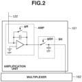
- Fig. 2 illustrates an example of a detailed circuit configuration of the amplification unit 161.
- the amplification unit 161 includes a differential amplification circuit AMP and a sample hold circuit SH.
- the differential amplification circuit AMP amplifies a signal appearing on the signal line 120 and outputs the amplified signal.
- the control unit 180 can reset the potential of the signal line 120 by supplying a control signal ⁇ R to a switch element of the differential amplification circuit AMP.
- the output from the differential amplification circuit AMP can be held by the sample hold circuit SH.
- the control unit 180 causes the sample hold circuit SH to hold the signal by supplying a control signal ⁇ SH to a switch element of the sample hold circuit SH.
- the signal held by the sample hold circuit SH is read out by the multiplexer 162.
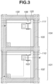
- Fig. 3 is a plan view of a configuration of each of the imaging pixel 101 and the detection pixel 104 in the radiation imaging apparatus 100.
- the plan view is equivalent to an orthographic projection on a plane parallel with the imaging region IR of the radiation imaging apparatus 100.
- Fig. 4 is a cross-sectional view of the imaging pixel 101 taken along a line A-A' in Fig. 3 .
- a cross sectional view of the detection pixel 104 is similar to the cross-sectional view of the imaging pixel 101.
- the switch element 103 is disposed on a supporting substrate 400 of insulation, such as a glass substrate.
- the switch element 103 can be a TFT.
- An interlayer insulation layer 401 is disposed on the switch element 103.
- the conversion element 102 is disposed on the interlayer insulation layer 401.
- the conversion element 102 is a photoelectric conversion element that can convert light into an electrical signal.
- the conversion element 102 includes, for example, an electrode 402, a PIN photodiode 403, and an electrode 404. Instead of the PIN-type photodiode, the conversion element 102 can be configured of a MIS-type sensor.
- the grid 600 is a sheet having a size close to the size of the radiation imaging apparatus 100 and is disposed between the object 700 and the radiation imaging apparatus 100.
- the grid 600 is used to remove scattered rays that have passed through the object 700.
- the grid 600 is disposed immediately in front of the radiation imaging apparatus 100.
- a dose, an emission upper limit time (millisecond (ms)), a tube current (milliampere (mA)), a tube voltage (kilovolt (kV)), a region of interest (ROI) that is an area where radiation is to be monitored, and the like are input into the controller 504.
- the controller 504 transmits a start request signal to the radiation imaging apparatus 100.
- the start request signal is a signal that requests a start of emission of radiation.
- the radiation imaging apparatus 100 starts preparation to receive radiation that will be emitted by the radiation source 501.
- the radiation imaging apparatus 100 transmits a start enable signal to the radiation source interface 502 via the communication interface 503.
- the start enable signal is a signal notifying that emission of radiation can be started.
- the radiation source interface 502 causes the radiation source 501 to start emission of radiation.
- the radiation imaging apparatus 100 transmits an end request signal to the radiation source interface 502 via the communication interface 503.
- the end request signal is a signal requesting an end of the emission of radiation.
- the radiation source interface 502 causes the radiation source 501 to end the emission of radiation.
- the control unit 180 determines the threshold for the dose, based on an input value of dose, a radiation emission intensity, a communication delay between units, a processing delay, and the like. Even in a case where the end request signal is not received, the radiation source 501 stops the emission of radiation when the radiation emission time reaches the input emission upper limit time.
- the radiation imaging apparatus 100 Upon stopping the emission of radiation, the radiation imaging apparatus 100 sequentially scans the driving lines 110 (the driving lines 110 except for the detection driving lines 111) to which the imaging pixels 101 are connected and reads out an image signal of each of the imaging pixels 101 using the reading circuit 160, whereby a radiation image is acquired. Electric charges accumulated in the detection pixel 104 are read out during the emission of radiation, but the signals from these pixels cannot be used to form a radiation image.
- the signal processing unit 170 of the radiation imaging apparatus 100 performs interpolation processing using the pixel values of the imaging pixels 101 around the detection pixels 104, whereby the pixel values at the positions of these pixels are interpolated.
- a dose of radiation emitted to a detection area is detected by reading out outputs of a plurality of radiation detection pixels in the detection area during emission of radiation. If an output of imaging pixels in the detection area approximately corresponds to an irradiated dose and the output of imaging pixels in the detection area is approximately equal to an output of the radiation detection pixels read out during the emission, it can be determined that the dose during image capturing is accurately detected, which means that the AEC can be accurately performed.
- a pixel size, an arrangement of the radiation detection pixels, and a grid density (grid pitch) there may be a disproportionate influence of attenuation on the output of the plurality of radiation detection pixels in a region of interest due to an X-ray absorption layer of a grid.
- the plurality of radiation detection pixels 104 in the detection area 800 is arranged in the entire detection area 800, and while there are various arrangement methods, an arrangement method that improves the accuracy of the AEC by reducing or suppressing the disproportionate influence of attenuation due to the X-ray absorption layer of the grid will be described with reference to Fig. 8 to Fig. 11 .
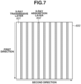
- Fig. 7 illustrates a configuration of the grid 600.
- the grid 600 includes a radiation transmissive layer (hereinafter referred to as the X-ray transmissive layer) 601 and a radiation absorption layer (hereinafter referred to as the X-ray absorption layer) 602 each having a strip shape which is elongated in a first direction (i.e. each strip substantially extends along the first direction), and the X-ray transmissive layer 601 and the X-ray absorption layer 602 are alternately arranged in a second direction which is orthogonal to the first direction.
- a radiation transmissive layer hereinafter referred to as the X-ray transmissive layer
- a radiation absorption layer hereinafter referred to as the X-ray absorption layer
- a grid density D which is the number of the X-ray absorption layers 602 per unit length is 32/centimeter (cm) to 100/cm, and a grid pitch is 100 micrometers ( ⁇ m) to about 300 ⁇ m.
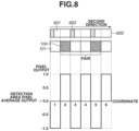
- Figs. 8 and 9 each illustrate an arrangement of the radiation detection pixels 104 of the grid in the second direction.
- Fig. 8 illustrates an arrangement and a pixel output of the radiation detection pixels 104 in a case where the pixel pitch is 125 ⁇ m, and the grid density is 40/cm (the grid pitch is 250 ⁇ m).
- the pixel output indicates a ratio of an output of each of the pixels to an average output of the pixels in the detection area.
- An output of each of the pixels is affected by a grid disposed in front of the radiation imaging apparatus. The influence of the grid on a pixel output varies depending on a pixel pitch and a grid density (grid pitch).
- the maximum value of the amplitude of the output O depends on a modulation transfer function (MTF) corresponding to the grid density (number/mm), the maximum value is fixed to 1 in the present invention for simplicity of description.
- the pixel pitch is half of the grid pitch, and thus, as the output of the pixels arranged in the second direction, an output (output -1) obtained with X-ray blocked by the X-ray absorption layer and an output (output 1) obtained with X-ray passed through the X-ray transmissive layer alternately appear in a cycle.
- Output signal values of the pair of the two radiation detection pixels are averaged, so that each other's grid influences are canceled, and the detection area pixel average output and the radiation detection pixel average output value become approximately equal, and thus the accuracy of the AEC can be improved by reducing or suppressing the influence of the grid.
- the output signal values of the pair of the detection pixels are offset by each other in terms of the influence of the attenuation by the grid and become approximately equal to a detection area pixel average value.
- being approximately equal to the average value means that differences of about 10% of the average value are included as an allowable range.
- the outputs of the radiation detection pixels can be used for the total value, instead of the average value.
- Fig. 10 illustrates a configuration of a second exemplary embodiment in which a plurality of pairs of radiation detection pixels 104 to reduce or suppress a grid influence is disposed in a detection area.
- Fig. 10 illustrates an arrangement and a pixel output of radiation detection pixels 104 in a case where a pixel pitch is 125 ⁇ m and a grid density is 40/cm (a grid pitch is 250 ⁇ m).
- a pair of radiation detection pixels 104 are disposed based on the equation (2), and a plurality of pairs of radiation detection pixels 104 is disposed at regular intervals.
- the influence of the grid is canceled by each pair of radiation detection pixels 104 (coordinates 2 and 5, coordinates 11 and 14, and coordinates 20 and 23), in accordance with the periodicity of the grid influence. Therefore, the grid influence on the output of the plurality of radiation detection pixels 104 in the detection area can be reduced or suppressed, whereby the accuracy of AEC can be improved.
- Fig. 11 illustrates a configuration in which a plurality of pairs of radiation detection pixels 104 to reduce or suppress a grid influence is disposed in a detection area.
- Fig. 11 illustrates an arrangement and a pixel output of radiation detection pixels 104 in a case where a pixel pitch is 125 ⁇ m and a grid density is 40/cm (a grid pitch is 250 ⁇ m).
- a pair of radiation detection pixels 104 are disposed based on the equation (2), and a plurality of pairs of radiation detection pixels 104 is disposed at different intervals.
- the influence of the grid is canceled by each pair of radiation detection pixels 104 (coordinates 2 and 5, coordinates 10 and 13, and coordinates 19 and 22), in accordance with the periodicity of the grid influence. Therefore, the grid influence on the output of the plurality of radiation detection pixels 104 in the detection area can be reduced or suppressed, whereby the accuracy of AEC can be improved.
- the case where the pairs of radiation detection pixels 104 are disposed at irregular intervals means a case where pairs of detection pixels are aperiodically arranged.
- An X-ray 6060 generated by an X-ray tube 6050 that is a radiation source passes through a chest 6062 of a patient or subject 6061 and is incident on a radiation imaging apparatus 6040 represented by the radiation imaging apparatus 100 described above.
- the incident X-ray includes information about the inside of the body of the subject 6061.
- the scintillator emits light in response to the incidence of the X-ray, and the photoelectric conversion element photoelectrically converts the light, whereby electrical information is obtained.
- the information is converted into digital information, and the digital information is subjected to image processing by an image processor 6070 that is a signal processing unit.
- the processed information is displayed on a display 6080 of a display unit in a control room, whereby the user can observe the image.
- the information can be transferred to a remote location by a transmission processing unit using, for example a telephone line 6090, and the transferred information can be displayed on a display 6081 of a display unit or saved into a recording unit, such as an optical disc, in an examination room at another place, which can allow a doctor to make diagnosis at the remote location.
- the information can also be recorded in a film 6110 that is a recording medium recorded by a film processor 6100 serving as a recording unit.
- the exemplary embodiments of the present invention it is possible to improve the accuracy of automatic exposure control, by reducing or suppressing a disproportionate influence on a signal of a radiation detection pixel due to attenuation by an X-ray absorption layer of a grid.
Landscapes
- Health & Medical Sciences (AREA)
- Life Sciences & Earth Sciences (AREA)
- Engineering & Computer Science (AREA)
- Medical Informatics (AREA)
- Physics & Mathematics (AREA)
- Molecular Biology (AREA)
- High Energy & Nuclear Physics (AREA)
- Heart & Thoracic Surgery (AREA)
- General Health & Medical Sciences (AREA)
- Pathology (AREA)
- Radiology & Medical Imaging (AREA)
- Biomedical Technology (AREA)
- Nuclear Medicine, Radiotherapy & Molecular Imaging (AREA)
- Biophysics (AREA)
- Surgery (AREA)
- Animal Behavior & Ethology (AREA)
- Optics & Photonics (AREA)
- Public Health (AREA)
- Veterinary Medicine (AREA)
- Mathematical Physics (AREA)
- Human Computer Interaction (AREA)
- Measurement Of Radiation (AREA)
- Apparatus For Radiation Diagnosis (AREA)
- X-Ray Techniques (AREA)
- General Physics & Mathematics (AREA)
- Spectroscopy & Molecular Physics (AREA)
Claims (4)
- Strahlungsbildgebungsvorrichtung (100) zum Durchführen von Radiographie unter Verwendung eines Gitters, in dem eine strahlungsdurchlässige Schicht und eine strahlungsabsorbierende Schicht, die jeweils streifenförmig sind und sich in einer ersten Richtung erstrecken, abwechselnd in einer zweiten Richtung angeordnet sind, wobei die Strahlungsbildgebungsvorrichtung umfasst:eine Pixeleinrichtung, die mehrere Bildgebungspixel (101) zum Erfassen eines Strahlungsbilds und mehrere Detektionspixel (104) zum Detektieren einer Strahlungsdosis enthält, die in einem Bildgebungsbereich angeordnet sind;eine Ansteuereinrichtung (150) zum Ansteuern der mehreren Bildgebungspixel (101) und der mehreren Detektionspixel (104);eine Leseeinrichtung (160) zum Auslesen eines Signals von einem jeweiligen der mehreren Bildgebungspixel (101) und der mehreren Detektionspixel (104); undeine Steuereinrichtung (180) zum Bestimmen einer Strahlungsmenge, die auf die Strahlungsbildgebungsvorrichtung emittiert wird,wobei die mehreren Detektionspixel ein erstes Detektionspixel und ein zweites Detektionspixel in der zweiten Richtung in einem Paar enthalten, ein Ausgangssignalwert des ersten Detektionspixels größer als ein Mittelwert von Ausgangssignalwerten der mehreren Bildgebungspixel und der mehreren Detektionspixel ist und ein Ausgangssignalwert des zweiten Detektionspixels kleiner als der Mittelwert ist, dadurch gekennzeichnet, dass mehrere Paare des ersten Detektionspixels und des zweiten Detektionspixels in einer aperiodischen Anordnung angeordnet sind.
- Strahlungsbildgebungsvorrichtung (100) nach Anspruch 1, wobei der Mittelwert der Ausgangssignalwerte der mehreren Bildgebungspixel und der mehreren Detektionspixel ein Mittelwert von Ausgangssignalwerten von Bildgebungspixeln und Detektionspixeln ist, die in einem Detektionsgebiet angeordnet sind, das ein Gebiet ist, in dem Strahlung detektiert wird.
- Strahlungsbildgebungsvorrichtung (100) nach Anspruch 1 oder 2, wobei ein Mittelwert der Ausgangssignalwerte des ersten Detektionspixels und des zweiten Detektionspixels gleich groß ist wie der Mittelwert der Ausgangssignalwerte der mehreren Bildgebungspixel und der mehreren Detektionspixel.
- Strahlungsbildgebungsvorrichtung (100) nach einem der Ansprüche 1 bis 3,wobei das erste Detektionspixel und das zweite Detektionspixel in der zweiten Richtung an jeweiligen Positionen angeordnet sind, die die folgende Gleichung erfüllen:
 wobei
wobei wobei C eine Position des zweiten Detektionspixels in Bezug auf das erste Detektionspixel darstellt, D eine Gitterdichte (Anzahl/Zentimeter) darstellt, P einen Pixelabstand (Millimeter) darstellt, k eine ganze Zahl darstellt, die 0 ≤ fg ≤ 1 erfüllt, und n eine ganze Zahl von 0 oder mehr darstellt.
Applications Claiming Priority (1)
| Application Number | Priority Date | Filing Date | Title |
|---|---|---|---|
| JP2021192186A JP2023078874A (ja) | 2021-11-26 | 2021-11-26 | 放射線撮像装置及び放射線撮像システム |
Publications (2)
| Publication Number | Publication Date |
|---|---|
| EP4186428A1 EP4186428A1 (de) | 2023-05-31 |
| EP4186428B1 true EP4186428B1 (de) | 2025-07-02 |
Family
ID=84246213
Family Applications (1)
| Application Number | Title | Priority Date | Filing Date |
|---|---|---|---|
| EP22205391.0A Active EP4186428B1 (de) | 2021-11-26 | 2022-11-03 | Strahlungsabbildungsvorrichtung |
Country Status (4)
| Country | Link |
|---|---|
| US (1) | US12329554B2 (de) |
| EP (1) | EP4186428B1 (de) |
| JP (1) | JP2023078874A (de) |
| CN (1) | CN116172585A (de) |
Families Citing this family (2)
| Publication number | Priority date | Publication date | Assignee | Title |
|---|---|---|---|---|
| JP2024075034A (ja) * | 2022-11-22 | 2024-06-03 | キヤノン株式会社 | 放射線撮像装置及び放射線撮像システム |
| US20240419051A1 (en) * | 2023-06-13 | 2024-12-19 | Look Dynamics, Inc. | Aperiodic optical sensors, modulators, and antennas |
Family Cites Families (3)
| Publication number | Priority date | Publication date | Assignee | Title |
|---|---|---|---|---|
| JP2012032645A (ja) * | 2010-07-30 | 2012-02-16 | Fujifilm Corp | 放射線撮影装置及び放射線撮影システム |
| JP5969950B2 (ja) * | 2012-04-20 | 2016-08-17 | 富士フイルム株式会社 | 放射線画像検出装置及び放射線撮影システム |
| JP5808365B2 (ja) * | 2012-07-27 | 2015-11-10 | 富士フイルム株式会社 | 放射線画像検出装置、並びに放射線撮影システムおよびその作動方法 |
-
2021
- 2021-11-26 JP JP2021192186A patent/JP2023078874A/ja active Pending
-
2022
- 2022-11-03 EP EP22205391.0A patent/EP4186428B1/de active Active
- 2022-11-11 US US18/054,836 patent/US12329554B2/en active Active
- 2022-11-16 CN CN202211432212.8A patent/CN116172585A/zh active Pending
Also Published As
| Publication number | Publication date |
|---|---|
| JP2023078874A (ja) | 2023-06-07 |
| EP4186428A1 (de) | 2023-05-31 |
| US12329554B2 (en) | 2025-06-17 |
| CN116172585A (zh) | 2023-05-30 |
| US20230168394A1 (en) | 2023-06-01 |
Similar Documents
| Publication | Publication Date | Title |
|---|---|---|
| CN111214250B (zh) | 放射线成像装置和放射线成像系统 | |
| US11090018B2 (en) | Radiation imaging apparatus, radiation imaging system, control method of radiation imaging apparatus, and non-transitory computer-readable storage medium | |
| JP5808365B2 (ja) | 放射線画像検出装置、並びに放射線撮影システムおよびその作動方法 | |
| US8879689B2 (en) | Radiographic image detecting device and control method thereof | |
| JP5890344B2 (ja) | 放射線画像検出装置及び放射線撮影システム | |
| JP5969950B2 (ja) | 放射線画像検出装置及び放射線撮影システム | |
| US11693131B2 (en) | Radiation imaging apparatus and radiation imaging system | |
| EP4186428B1 (de) | Strahlungsabbildungsvorrichtung | |
| JP7373338B2 (ja) | 放射線撮像装置及び放射線撮像システム | |
| JP2014003559A (ja) | 放射線画像撮影装置および放射線画像撮影システム | |
| US11831813B2 (en) | Apparatus, system, and method for controlling apparatus | |
| EP4075791B1 (de) | Strahlungsbildgebungsvorrichtung und strahlungsbildgebungssystem | |
| JP2017220403A (ja) | 放射線撮影システム、制御装置及びその制御方法、並びに、プログラム | |
| WO1999067657A1 (en) | X-ray based measuring device | |
| US9924113B2 (en) | Radiation imaging apparatus and radiation imaging system | |
| JP2006125872A (ja) | 放射線画像検出装置及び放射線画像撮影システム | |
| JP7438720B2 (ja) | 放射線撮像装置及び放射線撮像システム | |
| JP4501383B2 (ja) | X線撮影装置 | |
| JP7190360B2 (ja) | 放射線撮像装置および放射線撮像システム | |
| JP2018195949A (ja) | 放射線撮像装置及び放射線撮像システム | |
| US20240280715A1 (en) | Radiation imaging system | |
| WO2020162024A1 (ja) | 放射線撮像装置および放射線撮像システム | |
| EP3793189B1 (de) | Radiografievorrichtung und steuerungsverfahren dafür |
Legal Events
| Date | Code | Title | Description |
|---|---|---|---|
| PUAI | Public reference made under article 153(3) epc to a published international application that has entered the european phase |
Free format text: ORIGINAL CODE: 0009012 |
|
| STAA | Information on the status of an ep patent application or granted ep patent |
Free format text: STATUS: THE APPLICATION HAS BEEN PUBLISHED |
|
| AK | Designated contracting states |
Kind code of ref document: A1 Designated state(s): AL AT BE BG CH CY CZ DE DK EE ES FI FR GB GR HR HU IE IS IT LI LT LU LV MC ME MK MT NL NO PL PT RO RS SE SI SK SM TR |
|
| STAA | Information on the status of an ep patent application or granted ep patent |
Free format text: STATUS: REQUEST FOR EXAMINATION WAS MADE |
|
| 17P | Request for examination filed |
Effective date: 20231130 |
|
| RBV | Designated contracting states (corrected) |
Designated state(s): AL AT BE BG CH CY CZ DE DK EE ES FI FR GB GR HR HU IE IS IT LI LT LU LV MC ME MK MT NL NO PL PT RO RS SE SI SK SM TR |
|
| GRAP | Despatch of communication of intention to grant a patent |
Free format text: ORIGINAL CODE: EPIDOSNIGR1 |
|
| STAA | Information on the status of an ep patent application or granted ep patent |
Free format text: STATUS: GRANT OF PATENT IS INTENDED |
|
| INTG | Intention to grant announced |
Effective date: 20250203 |
|
| GRAS | Grant fee paid |
Free format text: ORIGINAL CODE: EPIDOSNIGR3 |
|
| GRAA | (expected) grant |
Free format text: ORIGINAL CODE: 0009210 |
|
| STAA | Information on the status of an ep patent application or granted ep patent |
Free format text: STATUS: THE PATENT HAS BEEN GRANTED |
|
| AK | Designated contracting states |
Kind code of ref document: B1 Designated state(s): AL AT BE BG CH CY CZ DE DK EE ES FI FR GB GR HR HU IE IS IT LI LT LU LV MC ME MK MT NL NO PL PT RO RS SE SI SK SM TR |
|
| REG | Reference to a national code |
Ref country code: GB Ref legal event code: FG4D |
|
| REG | Reference to a national code |
Ref country code: CH Ref legal event code: EP |
|
| REG | Reference to a national code |
Ref country code: DE Ref legal event code: R096 Ref document number: 602022016794 Country of ref document: DE |
|
| REG | Reference to a national code |
Ref country code: IE Ref legal event code: FG4D |
|
| REG | Reference to a national code |
Ref country code: NL Ref legal event code: MP Effective date: 20250702 |
|
| PG25 | Lapsed in a contracting state [announced via postgrant information from national office to epo] |
Ref country code: PT Free format text: LAPSE BECAUSE OF FAILURE TO SUBMIT A TRANSLATION OF THE DESCRIPTION OR TO PAY THE FEE WITHIN THE PRESCRIBED TIME-LIMIT Effective date: 20251103 |
|
| PG25 | Lapsed in a contracting state [announced via postgrant information from national office to epo] |
Ref country code: NL Free format text: LAPSE BECAUSE OF FAILURE TO SUBMIT A TRANSLATION OF THE DESCRIPTION OR TO PAY THE FEE WITHIN THE PRESCRIBED TIME-LIMIT Effective date: 20250702 |
|
| REG | Reference to a national code |
Ref country code: AT Ref legal event code: MK05 Ref document number: 1808311 Country of ref document: AT Kind code of ref document: T Effective date: 20250702 |
|
| PG25 | Lapsed in a contracting state [announced via postgrant information from national office to epo] |
Ref country code: IS Free format text: LAPSE BECAUSE OF FAILURE TO SUBMIT A TRANSLATION OF THE DESCRIPTION OR TO PAY THE FEE WITHIN THE PRESCRIBED TIME-LIMIT Effective date: 20251102 |
|
| PGFP | Annual fee paid to national office [announced via postgrant information from national office to epo] |
Ref country code: DE Payment date: 20251022 Year of fee payment: 4 |
|
| PG25 | Lapsed in a contracting state [announced via postgrant information from national office to epo] |
Ref country code: NO Free format text: LAPSE BECAUSE OF FAILURE TO SUBMIT A TRANSLATION OF THE DESCRIPTION OR TO PAY THE FEE WITHIN THE PRESCRIBED TIME-LIMIT Effective date: 20251002 |
|
| REG | Reference to a national code |
Ref country code: LT Ref legal event code: MG9D |
|
| PG25 | Lapsed in a contracting state [announced via postgrant information from national office to epo] |
Ref country code: AT Free format text: LAPSE BECAUSE OF FAILURE TO SUBMIT A TRANSLATION OF THE DESCRIPTION OR TO PAY THE FEE WITHIN THE PRESCRIBED TIME-LIMIT Effective date: 20250702 |
|
| PG25 | Lapsed in a contracting state [announced via postgrant information from national office to epo] |
Ref country code: FI Free format text: LAPSE BECAUSE OF FAILURE TO SUBMIT A TRANSLATION OF THE DESCRIPTION OR TO PAY THE FEE WITHIN THE PRESCRIBED TIME-LIMIT Effective date: 20250702 |
|
| PG25 | Lapsed in a contracting state [announced via postgrant information from national office to epo] |
Ref country code: HR Free format text: LAPSE BECAUSE OF FAILURE TO SUBMIT A TRANSLATION OF THE DESCRIPTION OR TO PAY THE FEE WITHIN THE PRESCRIBED TIME-LIMIT Effective date: 20250702 |
|
| PG25 | Lapsed in a contracting state [announced via postgrant information from national office to epo] |
Ref country code: GR Free format text: LAPSE BECAUSE OF FAILURE TO SUBMIT A TRANSLATION OF THE DESCRIPTION OR TO PAY THE FEE WITHIN THE PRESCRIBED TIME-LIMIT Effective date: 20251003 |
|
| PG25 | Lapsed in a contracting state [announced via postgrant information from national office to epo] |
Ref country code: SE Free format text: LAPSE BECAUSE OF FAILURE TO SUBMIT A TRANSLATION OF THE DESCRIPTION OR TO PAY THE FEE WITHIN THE PRESCRIBED TIME-LIMIT Effective date: 20250702 Ref country code: CZ Free format text: LAPSE BECAUSE OF FAILURE TO SUBMIT A TRANSLATION OF THE DESCRIPTION OR TO PAY THE FEE WITHIN THE PRESCRIBED TIME-LIMIT Effective date: 20250702 |
|
| PG25 | Lapsed in a contracting state [announced via postgrant information from national office to epo] |
Ref country code: LV Free format text: LAPSE BECAUSE OF FAILURE TO SUBMIT A TRANSLATION OF THE DESCRIPTION OR TO PAY THE FEE WITHIN THE PRESCRIBED TIME-LIMIT Effective date: 20250702 |
|
| PG25 | Lapsed in a contracting state [announced via postgrant information from national office to epo] |
Ref country code: BG Free format text: LAPSE BECAUSE OF FAILURE TO SUBMIT A TRANSLATION OF THE DESCRIPTION OR TO PAY THE FEE WITHIN THE PRESCRIBED TIME-LIMIT Effective date: 20250702 Ref country code: PL Free format text: LAPSE BECAUSE OF FAILURE TO SUBMIT A TRANSLATION OF THE DESCRIPTION OR TO PAY THE FEE WITHIN THE PRESCRIBED TIME-LIMIT Effective date: 20250702 |
|
| PG25 | Lapsed in a contracting state [announced via postgrant information from national office to epo] |
Ref country code: RS Free format text: LAPSE BECAUSE OF FAILURE TO SUBMIT A TRANSLATION OF THE DESCRIPTION OR TO PAY THE FEE WITHIN THE PRESCRIBED TIME-LIMIT Effective date: 20251002 |
|
| PG25 | Lapsed in a contracting state [announced via postgrant information from national office to epo] |
Ref country code: ES Free format text: LAPSE BECAUSE OF FAILURE TO SUBMIT A TRANSLATION OF THE DESCRIPTION OR TO PAY THE FEE WITHIN THE PRESCRIBED TIME-LIMIT Effective date: 20250702 |