EP4182996B1 - Kapazitive durchführung für hybride hermetische module für raumanwendungen - Google Patents
Kapazitive durchführung für hybride hermetische module für raumanwendungen Download PDFInfo
- Publication number
- EP4182996B1 EP4182996B1 EP21743281.4A EP21743281A EP4182996B1 EP 4182996 B1 EP4182996 B1 EP 4182996B1 EP 21743281 A EP21743281 A EP 21743281A EP 4182996 B1 EP4182996 B1 EP 4182996B1
- Authority
- EP
- European Patent Office
- Prior art keywords
- metallized
- layer
- metallized layer
- region
- layers
- Prior art date
- Legal status (The legal status is an assumption and is not a legal conclusion. Google has not performed a legal analysis and makes no representation as to the accuracy of the status listed.)
- Active
Links
Images



Classifications
-
- H—ELECTRICITY
- H01—ELECTRIC ELEMENTS
- H01P—WAVEGUIDES; RESONATORS, LINES, OR OTHER DEVICES OF THE WAVEGUIDE TYPE
- H01P1/00—Auxiliary devices
- H01P1/20—Frequency-selective devices, e.g. filters
- H01P1/2007—Filtering devices for biasing networks or DC returns
-
- H—ELECTRICITY
- H02—GENERATION; CONVERSION OR DISTRIBUTION OF ELECTRIC POWER
- H02G—INSTALLATION OF ELECTRIC CABLES OR LINES, OR OF COMBINED OPTICAL AND ELECTRIC CABLES OR LINES
- H02G3/00—Installations of electric cables or lines or protective tubing therefor in or on buildings, equivalent structures or vehicles
- H02G3/22—Installations of cables or lines through walls, floors or ceilings, e.g. into buildings
-
- B—PERFORMING OPERATIONS; TRANSPORTING
- B64—AIRCRAFT; AVIATION; COSMONAUTICS
- B64G—COSMONAUTICS; VEHICLES OR EQUIPMENT THEREFOR
- B64G1/00—Cosmonautic vehicles
- B64G1/22—Parts of, or equipment specially adapted for fitting in or to, cosmonautic vehicles
-
- H—ELECTRICITY
- H01—ELECTRIC ELEMENTS
- H01G—CAPACITORS; CAPACITORS, RECTIFIERS, DETECTORS, SWITCHING DEVICES, LIGHT-SENSITIVE OR TEMPERATURE-SENSITIVE DEVICES OF THE ELECTROLYTIC TYPE
- H01G4/00—Fixed capacitors; Processes of their manufacture
- H01G4/002—Details
- H01G4/005—Electrodes
- H01G4/012—Form of non-self-supporting electrodes
-
- H—ELECTRICITY
- H01—ELECTRIC ELEMENTS
- H01G—CAPACITORS; CAPACITORS, RECTIFIERS, DETECTORS, SWITCHING DEVICES, LIGHT-SENSITIVE OR TEMPERATURE-SENSITIVE DEVICES OF THE ELECTROLYTIC TYPE
- H01G4/00—Fixed capacitors; Processes of their manufacture
- H01G4/002—Details
- H01G4/228—Terminals
- H01G4/232—Terminals electrically connecting two or more layers of a stacked or rolled capacitor
-
- H—ELECTRICITY
- H01—ELECTRIC ELEMENTS
- H01G—CAPACITORS; CAPACITORS, RECTIFIERS, DETECTORS, SWITCHING DEVICES, LIGHT-SENSITIVE OR TEMPERATURE-SENSITIVE DEVICES OF THE ELECTROLYTIC TYPE
- H01G4/00—Fixed capacitors; Processes of their manufacture
- H01G4/30—Stacked capacitors
-
- H—ELECTRICITY
- H01—ELECTRIC ELEMENTS
- H01G—CAPACITORS; CAPACITORS, RECTIFIERS, DETECTORS, SWITCHING DEVICES, LIGHT-SENSITIVE OR TEMPERATURE-SENSITIVE DEVICES OF THE ELECTROLYTIC TYPE
- H01G4/00—Fixed capacitors; Processes of their manufacture
- H01G4/35—Feed-through capacitors or anti-noise capacitors
-
- H—ELECTRICITY
- H01—ELECTRIC ELEMENTS
- H01P—WAVEGUIDES; RESONATORS, LINES, OR OTHER DEVICES OF THE WAVEGUIDE TYPE
- H01P3/00—Waveguides; Transmission lines of the waveguide type
- H01P3/02—Waveguides; Transmission lines of the waveguide type with two longitudinal conductors
- H01P3/08—Microstrips; Strip lines
- H01P3/088—Stacked transmission lines
-
- H—ELECTRICITY
- H03—ELECTRONIC CIRCUITRY
- H03H—IMPEDANCE NETWORKS, e.g. RESONANT CIRCUITS; RESONATORS
- H03H1/00—Constructional details of impedance networks whose electrical mode of operation is not specified or applicable to more than one type of network
- H03H1/0007—Constructional details of impedance networks whose electrical mode of operation is not specified or applicable to more than one type of network of radio frequency interference filters
-
- H—ELECTRICITY
- H03—ELECTRONIC CIRCUITRY
- H03H—IMPEDANCE NETWORKS, e.g. RESONANT CIRCUITS; RESONATORS
- H03H1/00—Constructional details of impedance networks whose electrical mode of operation is not specified or applicable to more than one type of network
- H03H2001/0021—Constructional details
- H03H2001/0042—Wound, ring or feed-through type capacitor
Definitions
- the present invention relates, in general, to hermetically-sealed hybrid modules used for space applications (e.g., on board spacecraft, satellites, space platforms, etc.) and, more specifically, to a capacitive feedthrough that ensures electromagnetic interference (EMI) filtering and consequent electromagnetic compatibility (EMC) radiated emission performance adequate to hermetically-sealed hybrid modules, and that is hermetically sealable thereto.
- space applications e.g., on board spacecraft, satellites, space platforms, etc.
- EMC electromagnetic compatibility
- hybrid modules typically used to refer to a combination of elements (e.g., one or more interconnection substrates, one or more active or passive elements, etc.) arranged inside a hermetically sealed package/housing/casing and designed to perform one or more predefined electronic functions, wherein:
- Electromagnetic compatibility (EMC) radiated emission performance of a radiofrequency (RF) hybrid hermetic module is mainly determined by effectiveness of electromagnetic shielding of the module.
- RF radiofrequency
- a weak point of the electromagnetic shielding of hybrid modules is represented by direct current (DC) feedthroughs (i.e., elements designed and used to bring DC bias inside hybrid modules), which typically do not provide an adequate electromagnetic interference (EMI) filtering.
- DC direct current
- EMI electromagnetic interference
- US 2005/190527 A1 describes several feedthrough capacitor architectures for active implantable medical devices, wherein said feedthrough capacitor architectures are based on multilayer structures fitted with one or more hollow passageways provided with surface metallization and ending with metallized apertures on opposite faces of said multilayer structures.
- US 2005/190527 A1 discloses a feedthrough terminal assembly for an active implantable medical device, wherein said feedthrough terminal assembly comprises: a feedthrough capacitor having an aperture therethrough; first and second sets of electrode plates alternated with dielectric layers, the second set of electrode plates being conductively coupled to a housing of the active implantable medical device; a terminal pin extending at least partially through the aperture; a conductive insert disposed within the aperture for conductively coupling the terminal pin and the first set of electrode plates and for mechanically coupling the terminal pin to the feedthrough capacitor; and surface metallization within the aperture for conductively coupling the first set of electrode plates; wherein the conductive insert is disposed between and physically contacts the terminal pin and the interior aperture surface metallization.
- US 2005/190527 A1 states that the solution disclosed therein is theoretically applicable also to space electronic modules.
- the feedthrough capacitor architectures described in US 2005/190527 A1 do not actually provide EMI filtering performance suitable for space applications and require many elements, such as terminal pins, conductive inserts and conductive ferrules (necessary for signal propagation through the feedthrough capacitors), which complicate manufacturing process of such feedthrough capacitors.
- hermetic feedthrough for implantable medical devices is also disclosed in US 7 164 572 B1 , which relates to multi-path, mono-polar co-fired hermetic electrical feedthroughs and methods of fabrication therefor.
- the electrical feedthrough assembly according to US 7 164 572 B1 is not capacitive and is absolutely unsuitable for space applications.
- US 2002/166618 A1 relates to a capacitive filtered feedthrough array for an implantable medical device.
- US 2002/166618 A1 discloses a capacitive filtered feedthrough assembly formed in a solid state manner to employ highly miniaturized conductive paths, each filtered by a discoid capacitive filter embedded in a capacitive filter array.
- a nonconductive, co-fired metal-ceramic substrate is formed from multiple layers that supports one or a plurality of substrate conductive paths and it is brazed to a conductive ferrule, adapted to be welded to a case, using a conductive, corrosion resistant braze material.
- the metal-ceramic substrate is attached to an internally disposed capacitive filter array that encloses one or a plurality of capacitive filter capacitor active electrodes each coupled to a filter array conductive path and at least one capacitor ground electrode.
- Each capacitive filter array conductive path is joined with a metal-ceramic conductive path to form a feedthrough conductive path. Bonding pads are attached to the internally disposed ends of each feedthrough conductive path, and corrosion resistant, conductive buttons are attached to and seal the externally disposed ends of each feedthrough conductive path.
- a plurality of conductive, substrate ground paths are formed extending through the co-fired metal-ceramic substrate between internally and externally facing layer surfaces thereof and electrically isolated from the substrate conductive paths.
- the capacitor ground electrodes are coupled electrically to the plurality of conductive, substrate ground paths and to the ferrule.
- object of the present invention is that of providing a capacitive feedthrough for use with hybrid hermetic modules, in particular a capacitive feedthrough that ensures EMI filtering and consequent EMC radiated emission performance adequate to hybrid hermetic modules and that is hermetically sealable to a hybrid module for space applications.
- the hermetic assembly according to the present invention includes a hybrid hermetic module, and a capacitive feedthrough comprising a multilayer ceramic structure that has:
- said multilayer ceramic structure includes:
- the multilayer ceramic structure further includes ceramic layers, first metallized layers and one or more second metallized layers stacked on one another such that:
- the first metallized layers are joined to the metallized external closed side walls, whereby said first metallized layers, said metallized external closed side walls and said metallized top and bottom peripheral regions form an electrical ground structure.
- Each/the second metallized layer is separated from the metallized external closed side walls by a respective first dielectric gap designed to ensure electrical insulation between said second metallized layer and the electrical ground structure.
- Each/the second metallized layer is connected to:
- the metallized top and bottom central regions and the second metallized layer(s) along with the respective electrically conductive vias and the respective capacitors form a capacitive feedthrough structure configured to receive the input electrical signal at/on the metallized top central region and to provide the output filtered electrical signal at/on the metallized bottom central region, whereby filtering of the input electrical signal is carried out by the capacitors.
- the capacitive feedthrough is hermetically sealed to the hybrid hermetic module by means of a eutectic alloy.
- the present invention stems from Applicant's idea of using a multilayer ceramic substrate (preferably, a multilayer high temperature cofired ceramic (HTCC) or low temperature cofired ceramic (LTCC) substrate; conveniently, a multilayer HTCC/LTCC planar substrate) to make a capacitive feedthrough that provides EMI filtering and that can be hermetically sealed (conveniently, by means of a eutectic alloy) to an external wall of a hybrid module (in particular, an external wall of a housing/casing of a hybrid module), thereby resulting in an overall hermetic assembly provided with filtered DC bias access.
- a multilayer ceramic substrate preferably, a multilayer high temperature cofired ceramic (HTCC) or low temperature cofired ceramic (LTCC) substrate; conveniently, a multilayer HTCC/LTCC planar substrate
- HTCC high temperature cofired ceramic
- LTCC low temperature cofired ceramic
- the present invention concerns the use of a multilayer ceramic substrate to make a hermetic, EMI filtering, capacitive feedthrough device that is hermetically sealable to a hybrid hermetic module.
- Figures 1-4 schematically illustrate an example of capacitive feedthrough (denoted as a whole by 1) according to a preferred, non-limiting embodiment of the present invention.
- Figure 1 is a schematic perspective view of the capacitive feedthrough 1
- Figure 2 is a schematic top view thereof
- Figure 3 is a schematic bottom view thereof
- Figure 4 is a schematic vertical cross-sectional view thereof.
- said capacitive feedthrough 1 comprises a multilayer ceramic structure (preferably, a multilayer HTCC or LTCC structure; conveniently, a multilayer HTCC/LTCC planar substrate) that is conveniently shaped as a cube or a rectangular cuboid (more in general, it might have the shape of a parallelepiped, a hexahedron, a prism, or a polyhedron), and that has:
- the multilayer ceramic structure includes:
- the metallized top central region 11 is larger than the metallized bottom central region 21, whereas the metallized bottom peripheral region 23 is larger than the metallized top peripheral region 13.
- the multilayer ceramic structure includes eight (internal) ceramic layers and seven (internal) metallized layers (conveniently, made of metallized ceramic material; preferably, gold-metallized ceramic material) that are stacked on one another such that:
- the first, third, fifth and seventh metallized layers 51, 53, 55, 57 are joined/connected to the metallized external closed side walls 31, 32, 33, 34, whereby said first, third, fifth and seventh metallized layers 51, 53, 55, 57, said metallized external closed side walls 31, 32, 33, 34, said metallized top peripheral region 13 and said metallized bottom peripheral region 23 form an electrical ground structure.
- each of the second, fourth and sixth metallized layers 52, 54, 56 is separated from the metallized external closed side walls 31, 32, 33, 34 by a respective first dielectric gap (conveniently, made of non-metallized ceramic material) extending around said second/fourth/sixth metallized layer 52/54/56 between said second/fourth/sixth metallized layer 52/54/56 and the metallized external closed side walls 31, 32, 33, 34.
- first electrically conductive via 61 e.g., made of gold
- the fourth metallized layer 54 is electrically connected to the second metallized layer 52 by means of a second electrically conductive via 62 (e.g., made of gold), that:
- the sixth metallized layer 56 is electrically connected to the fourth metallized layer 54 by means of a third electrically conductive via 63 (e.g., made of gold), that:
- the sixth metallized layer 56 is electrically connected also to the metallized top central region 11 by means of a fourth electrically conductive via 64 (e.g., made of gold), that:
- the metallized top and bottom central regions 11, 21, the second, fourth and sixth metallized layers 52, 54, 56, the first, second, third and fourth electrically conductive vias 61, 62, 63, 64 and the corresponding first, second, third and fourth capacitors form a capacitive feedthrough structure configured to receive an input electrical signal (conveniently, a DC bias signal, such as an electrical voltage to be brought from outside to inside a hermetic hybrid) at/on the metallized top central region 11, and to output a corresponding filtered electrical signal at/on the metallized bottom central region 21, wherein the input electrical signal is filtered by said first, second, third and fourth capacitors.
- a DC bias signal such as an electrical voltage to be brought from outside to inside a hermetic hybrid
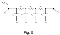
- Figure 5 shows a schematic circuit diagram of the capacitive feedthrough 1, including:
- an input electrical signal received at the input terminal/port P in is filtered by the shunt capacitors C 1 , C 2 , C 3 , C 4 , whereby a corresponding filtered electrical signal is provided at the output terminal/port P out .
- an EMI affecting a DC bias signal to be provided to a hybrid module is filtered out by the capacitive feedthrough 1, which is, thence, provided with the capability to supply a hybrid module with an EMI-free DC bias signal.
- the capacitive feedthrough 1 can be hermetically sealed to/on a wall of a housing/casing of a hybrid module by using a eutectic alloy having a predefined melting temperature (e.g., 300/320°C).
- Figure 6 schematically illustrates an example of hermetic sealing of the capacitive feedthrough 1 to a hybrid module.
- Figure 6 is a schematic vertical cross-sectional view of the capacitive feedthrough 1 embedded in a cavity formed on an external (metal) side wall (denoted by 70) of a (metal) housing/casing of a hybrid module (not shown in Figure 6 ).
- the capacitive feedthrough 1 is hermetically sealed to the hybrid module's external side wall 70 by means of a eutectic alloy 80 (e.g., a gold-tin (AuSn) alloy) that is:
- a eutectic alloy 80 e.g., a gold-tin (AuSn) alloy
- said capacitive feedthrough 1 is arranged/inserted in the cavity formed by the hybrid module's external side wall 70 such that the bottom face 20 faces towards the inside of the hybrid module, whereas the top face 10 faces towards the outside of said hybrid module.
- a wire (not shown in Figure 6 ) could be soldered onto the metallized top central region 11 (for example, by means of an indium-lead (InPb) solder alloy) to provide the capacitive feedthrough 1 with the input electrical signal to be filtered and, then, supplied to the hybrid module.
- an American wire gauge (AWG) wire might be conveniently used, whose diameter can be determined based on the current of the input electrical signal.
- a microwire (not shown in Figure 6 ) could be conveniently soldered onto the metallized bottom central region 21 (for example, by thermo-compression) to receive the filtered electrical signal provided by the capacitive feedthrough 1 (wherein the diameter of the microwire is smaller than the diameter of the wire soldered on the top face 10).
- the sealing of the capacitive feedthrough 1 might be conveniently based also on other alloys different than AuSn alloy (and having different melting temperatures), such as a gold-germanium (AuGe) alloy.
- AuGe gold-germanium
- the capacitive feedthrough 1 represents only a non-limiting example according to a preferred (again non-limiting) embodiment of the present invention.
- a capacitive feedthrough according to a more general embodiment of the present invention comprises a multilayer ceramic structure that has:
- said multilayer ceramic structure includes:
- the multilayer ceramic structure further includes (four or more) ceramic layers, (two or more) first metallized layers and one or more second metallized layers stacked on one another such that:
- the first metallized layers are joined to the metallized external closed side walls, whereby said first metallized layers, said metallized external closed side walls and said metallized top and bottom peripheral regions form an electrical ground structure.
- Each/the second metallized layer is separated from the metallized external closed side walls by a respective first dielectric gap designed to ensure electrical insulation between said second metallized layer and the electrical ground structure.
- Each/the second metallized layer is connected to:
- the metallized top and bottom central regions and the second metallized layer(s) along with the respective electrically conductive vias and the respective capacitors form a capacitive feedthrough structure configured to receive the input electrical signal at/on the metallized top central region and to provide the output filtered electrical signal at/on the metallized bottom central region, whereby filtering of the input electrical signal is carried out by the capacitors.
- the capacitive feedthrough according to the present invention can be advantageously used not only for DC signals, but also for low frequency signals, such as modulation signals.
- the capacitive feedthrough might be conveniently designed to perform a predefined low-pass filtering (e.g., up to 100 MHz), thereby enabling its use for both DC signals and low frequency signals (e.g., modulation signals).
- the present invention teaches to use a multilayer ceramic substrate (preferably, a multilayer HTCC/LTCC substrate; conveniently, a multilayer HTCC/LTCC planar substrate) that can be conveniently brazed on an external (metal) wall of a hybrid module (for example, at 320°C) without any reliability issue, thereby ensuring the hermetic sealing level required for space applications.
- a multilayer ceramic substrate preferably, a multilayer HTCC/LTCC substrate; conveniently, a multilayer HTCC/LTCC planar substrate
- a hybrid module for example, at 320°C
- the internal layers of the multilayer ceramic substrate are advantageously exploited to make a capacitive feedthrough structure (with metallic planes parallel to each other).
- the shape and the size of each internal metallic plane can be conveniently designed with a three-dimensional (3D) electromagnetic simulator in order to tune/optimize the filtering performed by the capacitive feedthrough (for example, as previously explained, to allow its use not only for DC signals, but also for low frequency signals, such as modulation signals).
- the use of a capacitive feedthrough structure based on a multilayer ceramic substrate as EMI filter hermetically sealed on the housing of a hybrid module to solve the issue of EMC/EMI shielding of the hybrid module is innovative, wherein the present invention enables device size miniaturization thanks to the reduced dimensions compared to conventional capacitive non-hermetic feedthroughs.
- the present invention allows conveniently using a parallelepiped-shaped multilayer HTCC substrate with 2.75 x 2.75 x 2.5 mm size, whereas conventional glass capacitive feedthroughs envelope dimensions are in the order of 4 x 4 x 20 mm.
- the capacitive feedthrough structure according to the present invention provides excellent EMI filtering performance, in particular EMI filtering performance adequate to space applications, and does not require the additional elements of said feedthrough capacitor architectures disclosed in US 2005/190527 A1 (such as hollow passageways with surface metallization and metallized apertures, terminal pins, conductive inserts and conductive ferrules), whereby the manufacturing process of the capacitive feedthrough structure according to the present invention is much simpler.
Landscapes
- Engineering & Computer Science (AREA)
- Power Engineering (AREA)
- Manufacturing & Machinery (AREA)
- Microelectronics & Electronic Packaging (AREA)
- Architecture (AREA)
- Civil Engineering (AREA)
- Structural Engineering (AREA)
- Aviation & Aerospace Engineering (AREA)
- Remote Sensing (AREA)
- Fixed Capacitors And Capacitor Manufacturing Machines (AREA)
- Shielding Devices Or Components To Electric Or Magnetic Fields (AREA)
- Ceramic Capacitors (AREA)
- Filters And Equalizers (AREA)
- Installation Of Indoor Wiring (AREA)
- Measuring Fluid Pressure (AREA)
Claims (13)
- Hermetische Anordnung für Raumanwendungen, die ein hybrides hermetisches Modul und eine kapazitive Durchführung (1), welche eine Mehrschichtkeramikstruktur aufweist, umfasst, die hat:• zwei entgegengesetzte Außenflächen, die eine obere Fläche (10) und eine untere Fläche (20) umfassen; und• metallisierte äußere geschlossene Seitenwände (31, 32, 33, 34), die sich zwischen den entgegengesetzten äußeren Flächen (10, 20) um die Mehrschichtkeramikstruktur herum erstrecken;wobei die Mehrschichtkeramikstruktur umfasst:• auf der oberen Fläche (10),- einen metallisierten oberen mittleren Bereich (11), der konzipiert ist, um ein elektrisches Eingangssignal, das gefiltert werden soll, zu empfangen,- einen dielektrischen oberen Bereich (12), der sich um den metallisierten oberen mittleren Bereich (11) herum erstreckt, und- einen metallisierten oberen Umfangsbereich (13), der sich um den dielektrischen oberen Bereich (12) herum bis zur Vereinigung der metallisierten äußeren geschlossenen Seitenwände (31, 32, 33, 34) erstreckt, um damit als elektrische Masse zu wirken, wobei der dielektrische obere Bereich (12) konzipiert ist, um die elektrische Isolierung zwischen dem elektrischen Eingangssignal und der elektrischen Masse sicherzustellen; und• auf der unteren Fläche (20):- einen metallisierten unteren mittleren Bereich (21), der konzipiert ist, um ein gefiltertes elektrisches Eingangssignal bereitzustellen,- einen dielektrischen unteren Bereich (22), der sich um den metallisierten unteren mittleren Bereich (21) herum erstreckt, und- einen metallisierten unteren Umfangsbereich (23), der sich um den dielektrischen unteren Bereich (22) herum bis zur Vereinigung der metallisierten äußeren geschlossenen Seitenwände (31, 32, 33, 34) erstreckt, um damit als elektrische Masse zu wirken, wobei der dielektrische untere Bereich (22) konzipiert ist, um die elektrische Isolierung zwischen dem gefilterten elektrischen Ausgangssignal und der elektrischen Masse sicherzustellen;wobei die Mehrschichtkeramikstruktur ferner keramische Schichten (41, 42, 43, 44, 45, 46, 47, 48), erste metallisierte Schichten (51, 53, 55, 57) und eine oder mehrere zweite metallisierte Schichten (52, 54, 56), die übereinander gestapelt sind, umfasst, so dass:• jede erste metallisierte Schicht (51, 53, 55, 57) zwischen zwei jeweiligen keramischen Schichten (41, 42, 43, 44, 45, 46, 47, 48), die unmittelbar auf und unter der ersten metallisierten Schicht (51, 53, 55, 57) angeordnet sind, eingefügt ist;• jede/die zweite metallisierte Schicht zwischen zwei jeweiligen keramischen Schichten (41, 42, 43, 44, 45, 46, 47), die unmittelbar auf und unter der zweiten metallisierten Schicht (52, 54, 56) angeordnet sind, eingefügt ist;• die ersten und zweiten metallisierten Schichten (51, 52, 53, 54, 55, 56, 57) vertikal abgewechselt werden, so dass jede/die zweite metallisierte Schicht (52, 54, 56) hat:- eine jeweilige obere erste metallisierte Schicht (53, 55, 57), die über der zweiten metallisierten Schicht (52, 54, 56) angeordnet ist, und- eine jeweilige untere erste metallisierte Schicht (51, 53, 55), die unterhalb der zweiten metallisierten Schicht (52, 54, 56) angeordnet ist; und• zwei keramische Schichten (41, 48) jeweils unmittelbar unter der oberen Fläche (10) und unmittelbar über der unteren Fläche (11) angeordnet sind,wobei die ersten metallisierten Schichten (51, 53, 55, 57) mit den metallisierten äußeren geschlossenen Seitenwänden (31, 32, 33, 34) verbunden sind, wodurch die ersten metallisierten Schichten (51, 53, 55, 57), die metallisierten äußeren geschlossenen Seitenwände (31, 32, 33, 34) und die metallisierten oberen und unteren Umfangsbereiche (13, 23) eine elektrische Massenstruktur bilden;wobei jede/die zweite metallisierte Schicht (52, 54, 56) von den metallisierten äußeren geschlossenen Seitenwänden (31, 32, 33, 34) durch eine jeweilige erste dielektrische Lücke getrennt ist, die konzipiert ist, um die elektrische Isolierung zwischen der zweiten metallisierten Schicht (52, 54, 56) und der elektrischen Massenstruktur sicherzustellen;wobei jede/die zweite metallisierte Schicht (52, 54, 56) verbunden ist mit:• einer oberen zweiten metallisierten Schicht (52, 54, 56) oder dem metallisierten oberen mittleren Bereich (11) mittels eines jeweiligen ersten elektrisch leitenden Kontaktlochs (62, 63, 64), das sich vertikal zwischen der zweiten metallisierten Schicht (52, 54, 56) und der oberen zweiten metallisierten Schicht (52, 54, 56)/dem metallisierten oberen mittleren Bereich (11) durch obere keramische Schichten (43, 44, 45, 46, 47, 48) und die jeweilige obere erste metallisierte Schicht (53, 55, 57) erstreckt, wobei das jeweilige erste elektrisch leitende Kontaktloch (62, 63, 64) von der jeweiligen oberen ersten metallisierten Schicht (53, 55, 57) durch eine jeweilige zweite dielektrische Lücke, die sich um das jeweilige erste elektrisch leitende Kontaktloch (62, 63, 64) herum erstreckt, getrennt ist, wodurch ein jeweiliger erster Kondensator ausgebildet wird; und• einer unteren zweiten metallisierten Schicht (52, 54, 56) oder dem metallisierten unteren mittleren Bereich (21) mittels eines jeweiligen zweiten elektrisch leitenden Kontaktlochs (61, 62, 63), das sich vertikal zwischen der zweiten metallisierten Schicht (52, 54, 56) und der unteren zweiten metallisierten Schicht (52, 54, 56)/dem metallisierten unteren mittleren Bereich (21) durch untere keramische Schichten (41, 42, 43, 44, 45, 46) und die jeweilige untere erste metallisierte Schicht (51, 53, 55) erstreckt, wobei das jeweilige zweite elektrisch leitende Kontaktloch (61, 62, 63) von der jeweiligen unteren ersten metallisierten Schicht (51, 53, 55) durch eine jeweilige dritte dielektrische Lücke, die sich um das jeweilige zweite elektrisch leitende Kontaktloch (61, 62, 63) herum erstreckt, getrennt ist, wodurch ein jeweiliger zweiter Kondensator ausgebildet wird;wobei die metallisierten oberen und unteren mittleren Bereiche (11, 21) und die zweiten metallisierten Schicht(en) (52, 54, 56) zusammen mit den jeweiligen elektrisch leitfähigen Kontaktlöchern (61, 62, 63, 64) und den jeweiligen Kondensatoren eine kapazitive Durchführungsstruktur ausbilden, die konfiguriert ist, um das elektrische Eingangssignal an/auf dem metallisierten oberen mittleren Bereich (11) zu empfangen und das gefilterte elektrische Ausgangssignal an/auf dem metallisierten unteren mittleren Bereich (21) auszugeben, wobei das Filtern des elektrischen Eingangssignals durch die Kondensatoren ausgeführt wird;und wobei die metallisierten oberen und unteren mittleren Bereiche (11, 21) planare Bereiche ohne Öffnungen sind;dadurch gekennzeichnet, dass die kapazitive Durchführung (1) zu dem hybriden hermetischen Modul mit Hilfe einer eutektischen Legierung (80) hermetisch abgedichtet ist.
- Hermetische Anordnung nach Anspruch 1, wobei der metallisierte obere mittlere Bereich (11) größer als der metallisierte untere mittlere Bereich (21) ist und der metallisierte untere Umfangsbereich (23) größer als der metallisierte obere Umfangsbereich (13) ist.
- Hermetische Anordnung nach Anspruch 1 oder 2, wobei die Mehrschichtkeramikstruktur vier oder mehr keramische Schichten (41, 42, 43, 44, 45, 46, 47, 48) und zwei oder mehr erste metallisierte Schichten (51, 53, 55, 57) umfasst.
- Hermetische Anordnung nach einem der Ansprüche 1 - 3, wobei die Mehrschichtkeramikstruktur ein gemeinsam gebranntes Hoch- oder Niedertemperaturkeramiksubstrat ist.
- Hermetische Anordnung nach Anspruch 4, wobei die Mehrschichtkeramikstruktur eine gemeinsam gebrannte planare Hoch-/Niedertemperaturkeramikstruktur ist.
- Hermetische Anordnung nach einem der vorhergehenden Ansprüche, wobei die metallisierten äußeren geschlossenen Seitenwände (31, 32, 33, 34), die metallisierten oberen und unteren mittleren Bereiche (11, 21), die metallisierten oberen und unteren Umfangsbereiche (13, 23) und die ersten und zweiten metallisierten Schichten (51, 52, 53, 54, 55, 56, 57) aus metallisiertem keramischem Material hergestellt sind.
- Hermetische Anordnung nach Anspruch 6, wobei die metallisierten äußeren geschlossenen Seitenwände (31, 32, 33, 34), die metallisierten oberen und unteren mittleren Bereiche (11, 21), die metallisierten oberen und unteren Umfangsbereiche (13, 23) und die ersten und zweiten metallisierten Schichten (51, 52, 53, 54, 55, 56, 57) aus mit Gold metallisiertem keramischem Material hergestellt sind.
- Hermetische Anordnung nach einem der vorhergehenden Ansprüche, wobei die dielektrischen oberen und unteren Bereiche (12, 22) aus nicht metallisiertem keramischem Material hergestellt sind; und wobei die jeweiligen ersten, zweiten und dritten Lücken für jede/die zweite metallisierte Schicht (52, 54, 56) aus nicht metallisiertem keramischem Material hergestellt sind.
- Hermetische Anordnung nach einem der vorhergehenden Ansprüche, wobei die jeweiligen elektrisch leitenden Kontaktlöcher (61, 62, 63, 64) für jede/die zweite metallisierte Schicht (52, 54, 56) aus Gold hergestellt sind.
- Hermetische Anordnung nach einem der vorhergehenden Ansprüche, wobei die kapazitive Durchführung (1) mit der kapazitiven Durchführung (1) hermetisch abgedichtet ist, so dass die untere Fläche (20) der kapazitiven Durchführung (1) in Richtung des Inneren des hybriden Moduls gewandt ist und die obere Fläche (10) der kapazitiven Durchführung (1) in Richtung des Äußeren des hybriden Moduls gewandt ist.
- Hermetische Anordnung nach einem der vorhergehenden Ansprüche, wobei die eutektische Legierung (80) eine Gold-Zinn- oder Gold-Germanium-Legierung ist.
- Raumplattform, welche die hermetische Anordnung nach einem der vorhergehenden Ansprüche umfasst.
- Raumplattform nach Anspruch 12, wobei die Raumplattform ein Satellit, ein Raumflugkörper, eine Raumstation oder ein Raumfahrzeug ist.
Priority Applications (1)
| Application Number | Priority Date | Filing Date | Title |
|---|---|---|---|
| SI202130155T SI4182996T1 (sl) | 2020-07-20 | 2021-07-20 | Kapacitivni skoznik za hibridne hermetične module za uporabo v vesolju |
Applications Claiming Priority (2)
| Application Number | Priority Date | Filing Date | Title |
|---|---|---|---|
| IT102020000017554A IT202000017554A1 (it) | 2020-07-20 | 2020-07-20 | Feedthrough capacitivo per moduli ermetici ibridi |
| PCT/IB2021/056550 WO2022018634A1 (en) | 2020-07-20 | 2021-07-20 | Capacitive feedthrough for hybrid hermetic modules for space applications |
Publications (2)
| Publication Number | Publication Date |
|---|---|
| EP4182996A1 EP4182996A1 (de) | 2023-05-24 |
| EP4182996B1 true EP4182996B1 (de) | 2024-05-08 |
Family
ID=72644830
Family Applications (1)
| Application Number | Title | Priority Date | Filing Date |
|---|---|---|---|
| EP21743281.4A Active EP4182996B1 (de) | 2020-07-20 | 2021-07-20 | Kapazitive durchführung für hybride hermetische module für raumanwendungen |
Country Status (7)
| Country | Link |
|---|---|
| US (1) | US12418165B2 (de) |
| EP (1) | EP4182996B1 (de) |
| JP (1) | JP7817233B2 (de) |
| ES (1) | ES2983209T3 (de) |
| IT (1) | IT202000017554A1 (de) |
| SI (1) | SI4182996T1 (de) |
| WO (1) | WO2022018634A1 (de) |
Family Cites Families (12)
| Publication number | Priority date | Publication date | Assignee | Title |
|---|---|---|---|---|
| JP2971993B2 (ja) * | 1991-06-25 | 1999-11-08 | 株式会社トーキン | 積層セラミックコンデンサ |
| JPH0864465A (ja) * | 1994-08-25 | 1996-03-08 | Tokin Corp | 積層セラミック部品の製造方法 |
| US5994975A (en) * | 1998-04-28 | 1999-11-30 | Trw Inc. | Millimeter wave ceramic-metal feedthroughs |
| US6414835B1 (en) * | 2000-03-01 | 2002-07-02 | Medtronic, Inc. | Capacitive filtered feedthrough array for an implantable medical device |
| US6987660B2 (en) * | 2003-02-27 | 2006-01-17 | Greatbatch-Sierra, Inc. | Spring contact system for EMI filtered hermetic seals for active implantable medical devices |
| US7038900B2 (en) * | 2003-02-27 | 2006-05-02 | Greatbatch-Sierra, Inc. | EMI filter terminal assembly with wire bond pads for human implant applications |
| JP2006032747A (ja) * | 2004-07-20 | 2006-02-02 | Ngk Spark Plug Co Ltd | 積層電子部品及びその製造方法 |
| US7164572B1 (en) * | 2005-09-15 | 2007-01-16 | Medtronic, Inc. | Multi-path, mono-polar co-fired hermetic electrical feedthroughs and methods of fabrication therfor |
| EP2371418B1 (de) * | 2010-03-29 | 2021-11-03 | BIOTRONIK SE & Co. KG | Elektrische Durchführung für elektromedizinische Implantate |
| US10596369B2 (en) * | 2011-03-01 | 2020-03-24 | Greatbatch Ltd. | Low equivalent series resistance RF filter for an active implantable medical device |
| EP3366348B1 (de) * | 2012-01-16 | 2023-08-23 | Greatbatch Ltd. | Emi-gefilterte co-verbundene hermetische durchführung, durchführungskondensator und leitungsanordnung für eine aktive implantierbare medizinische vorrichtung |
| US9935166B2 (en) * | 2013-03-15 | 2018-04-03 | Qualcomm Incorporated | Capacitor with a dielectric between a via and a plate of the capacitor |
-
2020
- 2020-07-20 IT IT102020000017554A patent/IT202000017554A1/it unknown
-
2021
- 2021-07-20 JP JP2023504068A patent/JP7817233B2/ja active Active
- 2021-07-20 ES ES21743281T patent/ES2983209T3/es active Active
- 2021-07-20 SI SI202130155T patent/SI4182996T1/sl unknown
- 2021-07-20 US US18/017,310 patent/US12418165B2/en active Active
- 2021-07-20 WO PCT/IB2021/056550 patent/WO2022018634A1/en not_active Ceased
- 2021-07-20 EP EP21743281.4A patent/EP4182996B1/de active Active
Also Published As
| Publication number | Publication date |
|---|---|
| IT202000017554A1 (it) | 2022-01-20 |
| WO2022018634A1 (en) | 2022-01-27 |
| EP4182996A1 (de) | 2023-05-24 |
| ES2983209T3 (es) | 2024-10-22 |
| JP2023535903A (ja) | 2023-08-22 |
| US20230291191A1 (en) | 2023-09-14 |
| SI4182996T1 (sl) | 2024-07-31 |
| JP7817233B2 (ja) | 2026-02-18 |
| US12418165B2 (en) | 2025-09-16 |
Similar Documents
| Publication | Publication Date | Title |
|---|---|---|
| JP4188373B2 (ja) | 多層誘電体基板および半導体パッケージ | |
| US7970474B2 (en) | Filter feedthrough for implants | |
| US20040080917A1 (en) | Integrated microwave package and the process for making the same | |
| US5602421A (en) | Microwave monolithic integrated circuit package with improved RF ports | |
| EP2428989B1 (de) | Hochfrequenzschaltungsgehäuse und Hochfrequenzschaltung | |
| US5451818A (en) | Millimeter wave ceramic package | |
| US8222976B2 (en) | Multilayer dielectric substrate and semiconductor package | |
| US5117068A (en) | Surface mount package for R.F. devices | |
| JPH03502986A (ja) | マイクロ波およびミリメータ波砒化ガリウム集積回路用の低温度共焼成セラミックパッケージ | |
| EP3113218B1 (de) | Gehäuse für ein elektronisches bauteil und elektronische vorrichtung mit dem gehäuse | |
| JPH1174396A (ja) | 高周波用入出力端子ならびに高周波用半導体素子収納用パッケージ | |
| US20250070809A1 (en) | Radio frequency module | |
| US20070203530A1 (en) | Filtered multipolar feedthrough assembly | |
| JP2006511071A (ja) | 表面実装を伴うマイクロ波パッケージ、および多層回路を備えた対応する実装体 | |
| JP3201681B2 (ja) | 表面実装型混成集積回路装置 | |
| US12418165B2 (en) | Capacitive feedthrough for hybrid hermetic modules for space applications | |
| US6140698A (en) | Package for microwave and mm-wave integrated circuits | |
| JP2007243989A (ja) | 弾性表面波フィルタパッケージ | |
| EP0235503B1 (de) | Hermetische, mikroelektronische Hochfrequenzpackung für Oberflächenmontage | |
| JPH0210756A (ja) | マイクロウェーブ・チップの相互接続及び保護のためのデバイス | |
| JP3152138B2 (ja) | 弾性表面波装置 | |
| EP2187520B1 (de) | Gehäuse für piezoelektrischen Resonator | |
| CN214625336U (zh) | 一种抑制倍频谐波的介质带通滤波器组件 | |
| US20250070805A1 (en) | Radio frequency module | |
| EP4356476B1 (de) | Auf metall-diamant-verbundstoff basierendes hochfrequenzwellenleitergehäuse |
Legal Events
| Date | Code | Title | Description |
|---|---|---|---|
| STAA | Information on the status of an ep patent application or granted ep patent |
Free format text: STATUS: UNKNOWN |
|
| STAA | Information on the status of an ep patent application or granted ep patent |
Free format text: STATUS: THE INTERNATIONAL PUBLICATION HAS BEEN MADE |
|
| PUAI | Public reference made under article 153(3) epc to a published international application that has entered the european phase |
Free format text: ORIGINAL CODE: 0009012 |
|
| STAA | Information on the status of an ep patent application or granted ep patent |
Free format text: STATUS: REQUEST FOR EXAMINATION WAS MADE |
|
| 17P | Request for examination filed |
Effective date: 20230124 |
|
| AK | Designated contracting states |
Kind code of ref document: A1 Designated state(s): AL AT BE BG CH CY CZ DE DK EE ES FI FR GB GR HR HU IE IS IT LI LT LU LV MC MK MT NL NO PL PT RO RS SE SI SK SM TR |
|
| P01 | Opt-out of the competence of the unified patent court (upc) registered |
Effective date: 20230601 |
|
| DAV | Request for validation of the european patent (deleted) | ||
| DAX | Request for extension of the european patent (deleted) | ||
| GRAP | Despatch of communication of intention to grant a patent |
Free format text: ORIGINAL CODE: EPIDOSNIGR1 |
|
| STAA | Information on the status of an ep patent application or granted ep patent |
Free format text: STATUS: GRANT OF PATENT IS INTENDED |
|
| RIC1 | Information provided on ipc code assigned before grant |
Ipc: H01G 4/30 20060101ALI20231121BHEP Ipc: H01G 4/232 20060101ALI20231121BHEP Ipc: H01G 4/012 20060101ALI20231121BHEP Ipc: H01P 3/08 20060101ALI20231121BHEP Ipc: H03H 1/00 20060101ALI20231121BHEP Ipc: H01G 4/35 20060101ALI20231121BHEP Ipc: H05K 1/02 20060101ALI20231121BHEP Ipc: H01P 1/20 20060101AFI20231121BHEP |
|
| INTG | Intention to grant announced |
Effective date: 20231206 |
|
| GRAS | Grant fee paid |
Free format text: ORIGINAL CODE: EPIDOSNIGR3 |
|
| GRAA | (expected) grant |
Free format text: ORIGINAL CODE: 0009210 |
|
| STAA | Information on the status of an ep patent application or granted ep patent |
Free format text: STATUS: THE PATENT HAS BEEN GRANTED |
|
| AK | Designated contracting states |
Kind code of ref document: B1 Designated state(s): AL AT BE BG CH CY CZ DE DK EE ES FI FR GB GR HR HU IE IS IT LI LT LU LV MC MK MT NL NO PL PT RO RS SE SI SK SM TR |
|
| REG | Reference to a national code |
Ref country code: GB Ref legal event code: FG4D |
|
| REG | Reference to a national code |
Ref country code: CH Ref legal event code: EP |
|
| REG | Reference to a national code |
Ref country code: DE Ref legal event code: R096 Ref document number: 602021013118 Country of ref document: DE |
|
| REG | Reference to a national code |
Ref country code: IE Ref legal event code: FG4D |
|
| REG | Reference to a national code |
Ref country code: SE Ref legal event code: TRGR |
|
| REG | Reference to a national code |
Ref country code: NL Ref legal event code: FP |
|
| REG | Reference to a national code |
Ref country code: LT Ref legal event code: MG9D |
|
| PG25 | Lapsed in a contracting state [announced via postgrant information from national office to epo] |
Ref country code: IS Free format text: LAPSE BECAUSE OF FAILURE TO SUBMIT A TRANSLATION OF THE DESCRIPTION OR TO PAY THE FEE WITHIN THE PRESCRIBED TIME-LIMIT Effective date: 20240908 |
|
| PG25 | Lapsed in a contracting state [announced via postgrant information from national office to epo] |
Ref country code: BG Free format text: LAPSE BECAUSE OF FAILURE TO SUBMIT A TRANSLATION OF THE DESCRIPTION OR TO PAY THE FEE WITHIN THE PRESCRIBED TIME-LIMIT Effective date: 20240508 |
|
| PG25 | Lapsed in a contracting state [announced via postgrant information from national office to epo] |
Ref country code: FI Free format text: LAPSE BECAUSE OF FAILURE TO SUBMIT A TRANSLATION OF THE DESCRIPTION OR TO PAY THE FEE WITHIN THE PRESCRIBED TIME-LIMIT Effective date: 20240508 Ref country code: HR Free format text: LAPSE BECAUSE OF FAILURE TO SUBMIT A TRANSLATION OF THE DESCRIPTION OR TO PAY THE FEE WITHIN THE PRESCRIBED TIME-LIMIT Effective date: 20240508 |
|
| PG25 | Lapsed in a contracting state [announced via postgrant information from national office to epo] |
Ref country code: GR Free format text: LAPSE BECAUSE OF FAILURE TO SUBMIT A TRANSLATION OF THE DESCRIPTION OR TO PAY THE FEE WITHIN THE PRESCRIBED TIME-LIMIT Effective date: 20240809 |
|
| PG25 | Lapsed in a contracting state [announced via postgrant information from national office to epo] |
Ref country code: PT Free format text: LAPSE BECAUSE OF FAILURE TO SUBMIT A TRANSLATION OF THE DESCRIPTION OR TO PAY THE FEE WITHIN THE PRESCRIBED TIME-LIMIT Effective date: 20240909 |
|
| REG | Reference to a national code |
Ref country code: AT Ref legal event code: MK05 Ref document number: 1685788 Country of ref document: AT Kind code of ref document: T Effective date: 20240508 |
|
| REG | Reference to a national code |
Ref country code: ES Ref legal event code: FG2A Ref document number: 2983209 Country of ref document: ES Kind code of ref document: T3 Effective date: 20241022 |
|
| PG25 | Lapsed in a contracting state [announced via postgrant information from national office to epo] |
Ref country code: AT Free format text: LAPSE BECAUSE OF FAILURE TO SUBMIT A TRANSLATION OF THE DESCRIPTION OR TO PAY THE FEE WITHIN THE PRESCRIBED TIME-LIMIT Effective date: 20240508 |
|
| PG25 | Lapsed in a contracting state [announced via postgrant information from national office to epo] |
Ref country code: PL Free format text: LAPSE BECAUSE OF FAILURE TO SUBMIT A TRANSLATION OF THE DESCRIPTION OR TO PAY THE FEE WITHIN THE PRESCRIBED TIME-LIMIT Effective date: 20240508 |
|
| PG25 | Lapsed in a contracting state [announced via postgrant information from national office to epo] |
Ref country code: LV Free format text: LAPSE BECAUSE OF FAILURE TO SUBMIT A TRANSLATION OF THE DESCRIPTION OR TO PAY THE FEE WITHIN THE PRESCRIBED TIME-LIMIT Effective date: 20240508 |
|
| PG25 | Lapsed in a contracting state [announced via postgrant information from national office to epo] |
Ref country code: PT Free format text: LAPSE BECAUSE OF FAILURE TO SUBMIT A TRANSLATION OF THE DESCRIPTION OR TO PAY THE FEE WITHIN THE PRESCRIBED TIME-LIMIT Effective date: 20240909 Ref country code: PL Free format text: LAPSE BECAUSE OF FAILURE TO SUBMIT A TRANSLATION OF THE DESCRIPTION OR TO PAY THE FEE WITHIN THE PRESCRIBED TIME-LIMIT Effective date: 20240508 Ref country code: LV Free format text: LAPSE BECAUSE OF FAILURE TO SUBMIT A TRANSLATION OF THE DESCRIPTION OR TO PAY THE FEE WITHIN THE PRESCRIBED TIME-LIMIT Effective date: 20240508 Ref country code: IS Free format text: LAPSE BECAUSE OF FAILURE TO SUBMIT A TRANSLATION OF THE DESCRIPTION OR TO PAY THE FEE WITHIN THE PRESCRIBED TIME-LIMIT Effective date: 20240908 Ref country code: HR Free format text: LAPSE BECAUSE OF FAILURE TO SUBMIT A TRANSLATION OF THE DESCRIPTION OR TO PAY THE FEE WITHIN THE PRESCRIBED TIME-LIMIT Effective date: 20240508 Ref country code: GR Free format text: LAPSE BECAUSE OF FAILURE TO SUBMIT A TRANSLATION OF THE DESCRIPTION OR TO PAY THE FEE WITHIN THE PRESCRIBED TIME-LIMIT Effective date: 20240809 Ref country code: FI Free format text: LAPSE BECAUSE OF FAILURE TO SUBMIT A TRANSLATION OF THE DESCRIPTION OR TO PAY THE FEE WITHIN THE PRESCRIBED TIME-LIMIT Effective date: 20240508 Ref country code: BG Free format text: LAPSE BECAUSE OF FAILURE TO SUBMIT A TRANSLATION OF THE DESCRIPTION OR TO PAY THE FEE WITHIN THE PRESCRIBED TIME-LIMIT Effective date: 20240508 Ref country code: AT Free format text: LAPSE BECAUSE OF FAILURE TO SUBMIT A TRANSLATION OF THE DESCRIPTION OR TO PAY THE FEE WITHIN THE PRESCRIBED TIME-LIMIT Effective date: 20240508 Ref country code: RS Free format text: LAPSE BECAUSE OF FAILURE TO SUBMIT A TRANSLATION OF THE DESCRIPTION OR TO PAY THE FEE WITHIN THE PRESCRIBED TIME-LIMIT Effective date: 20240808 |
|
| PG25 | Lapsed in a contracting state [announced via postgrant information from national office to epo] |
Ref country code: DK Free format text: LAPSE BECAUSE OF FAILURE TO SUBMIT A TRANSLATION OF THE DESCRIPTION OR TO PAY THE FEE WITHIN THE PRESCRIBED TIME-LIMIT Effective date: 20240508 |
|
| PG25 | Lapsed in a contracting state [announced via postgrant information from national office to epo] |
Ref country code: EE Free format text: LAPSE BECAUSE OF FAILURE TO SUBMIT A TRANSLATION OF THE DESCRIPTION OR TO PAY THE FEE WITHIN THE PRESCRIBED TIME-LIMIT Effective date: 20240508 |
|
| PG25 | Lapsed in a contracting state [announced via postgrant information from national office to epo] |
Ref country code: CZ Free format text: LAPSE BECAUSE OF FAILURE TO SUBMIT A TRANSLATION OF THE DESCRIPTION OR TO PAY THE FEE WITHIN THE PRESCRIBED TIME-LIMIT Effective date: 20240508 |
|
| PG25 | Lapsed in a contracting state [announced via postgrant information from national office to epo] |
Ref country code: SK Free format text: LAPSE BECAUSE OF FAILURE TO SUBMIT A TRANSLATION OF THE DESCRIPTION OR TO PAY THE FEE WITHIN THE PRESCRIBED TIME-LIMIT Effective date: 20240508 Ref country code: RO Free format text: LAPSE BECAUSE OF FAILURE TO SUBMIT A TRANSLATION OF THE DESCRIPTION OR TO PAY THE FEE WITHIN THE PRESCRIBED TIME-LIMIT Effective date: 20240508 |
|
| PG25 | Lapsed in a contracting state [announced via postgrant information from national office to epo] |
Ref country code: SM Free format text: LAPSE BECAUSE OF FAILURE TO SUBMIT A TRANSLATION OF THE DESCRIPTION OR TO PAY THE FEE WITHIN THE PRESCRIBED TIME-LIMIT Effective date: 20240508 |
|
| PG25 | Lapsed in a contracting state [announced via postgrant information from national office to epo] |
Ref country code: SM Free format text: LAPSE BECAUSE OF FAILURE TO SUBMIT A TRANSLATION OF THE DESCRIPTION OR TO PAY THE FEE WITHIN THE PRESCRIBED TIME-LIMIT Effective date: 20240508 Ref country code: SK Free format text: LAPSE BECAUSE OF FAILURE TO SUBMIT A TRANSLATION OF THE DESCRIPTION OR TO PAY THE FEE WITHIN THE PRESCRIBED TIME-LIMIT Effective date: 20240508 Ref country code: RO Free format text: LAPSE BECAUSE OF FAILURE TO SUBMIT A TRANSLATION OF THE DESCRIPTION OR TO PAY THE FEE WITHIN THE PRESCRIBED TIME-LIMIT Effective date: 20240508 Ref country code: EE Free format text: LAPSE BECAUSE OF FAILURE TO SUBMIT A TRANSLATION OF THE DESCRIPTION OR TO PAY THE FEE WITHIN THE PRESCRIBED TIME-LIMIT Effective date: 20240508 Ref country code: DK Free format text: LAPSE BECAUSE OF FAILURE TO SUBMIT A TRANSLATION OF THE DESCRIPTION OR TO PAY THE FEE WITHIN THE PRESCRIBED TIME-LIMIT Effective date: 20240508 Ref country code: CZ Free format text: LAPSE BECAUSE OF FAILURE TO SUBMIT A TRANSLATION OF THE DESCRIPTION OR TO PAY THE FEE WITHIN THE PRESCRIBED TIME-LIMIT Effective date: 20240508 |
|
| PG25 | Lapsed in a contracting state [announced via postgrant information from national office to epo] |
Ref country code: MC Free format text: LAPSE BECAUSE OF FAILURE TO SUBMIT A TRANSLATION OF THE DESCRIPTION OR TO PAY THE FEE WITHIN THE PRESCRIBED TIME-LIMIT Effective date: 20240508 |
|
| REG | Reference to a national code |
Ref country code: DE Ref legal event code: R097 Ref document number: 602021013118 Country of ref document: DE |
|
| REG | Reference to a national code |
Ref country code: CH Ref legal event code: PL |
|
| PLBE | No opposition filed within time limit |
Free format text: ORIGINAL CODE: 0009261 |
|
| STAA | Information on the status of an ep patent application or granted ep patent |
Free format text: STATUS: NO OPPOSITION FILED WITHIN TIME LIMIT |
|
| PG25 | Lapsed in a contracting state [announced via postgrant information from national office to epo] |
Ref country code: LU Free format text: LAPSE BECAUSE OF NON-PAYMENT OF DUE FEES Effective date: 20240720 |
|
| PG25 | Lapsed in a contracting state [announced via postgrant information from national office to epo] |
Ref country code: LU Free format text: LAPSE BECAUSE OF NON-PAYMENT OF DUE FEES Effective date: 20240720 |
|
| 26N | No opposition filed |
Effective date: 20250211 |
|
| PG25 | Lapsed in a contracting state [announced via postgrant information from national office to epo] |
Ref country code: CH Free format text: LAPSE BECAUSE OF NON-PAYMENT OF DUE FEES Effective date: 20240731 Ref country code: BE Free format text: LAPSE BECAUSE OF NON-PAYMENT OF DUE FEES Effective date: 20240731 |
|
| REG | Reference to a national code |
Ref country code: BE Ref legal event code: MM Effective date: 20240731 |
|
| PG25 | Lapsed in a contracting state [announced via postgrant information from national office to epo] |
Ref country code: IE Free format text: LAPSE BECAUSE OF NON-PAYMENT OF DUE FEES Effective date: 20240720 |
|
| PGFP | Annual fee paid to national office [announced via postgrant information from national office to epo] |
Ref country code: SI Payment date: 20250701 Year of fee payment: 5 |
|
| PGFP | Annual fee paid to national office [announced via postgrant information from national office to epo] |
Ref country code: NL Payment date: 20250724 Year of fee payment: 5 |
|
| PGFP | Annual fee paid to national office [announced via postgrant information from national office to epo] |
Ref country code: ES Payment date: 20250811 Year of fee payment: 5 |
|
| PGFP | Annual fee paid to national office [announced via postgrant information from national office to epo] |
Ref country code: DE Payment date: 20250728 Year of fee payment: 5 |
|
| PGFP | Annual fee paid to national office [announced via postgrant information from national office to epo] |
Ref country code: NO Payment date: 20250718 Year of fee payment: 5 |
|
| PGFP | Annual fee paid to national office [announced via postgrant information from national office to epo] |
Ref country code: IT Payment date: 20250627 Year of fee payment: 5 |
|
| PGFP | Annual fee paid to national office [announced via postgrant information from national office to epo] |
Ref country code: GB Payment date: 20250722 Year of fee payment: 5 |
|
| PGFP | Annual fee paid to national office [announced via postgrant information from national office to epo] |
Ref country code: FR Payment date: 20250725 Year of fee payment: 5 |
|
| PGFP | Annual fee paid to national office [announced via postgrant information from national office to epo] |
Ref country code: SE Payment date: 20250725 Year of fee payment: 5 |
|
| PG25 | Lapsed in a contracting state [announced via postgrant information from national office to epo] |
Ref country code: CY Free format text: LAPSE BECAUSE OF FAILURE TO SUBMIT A TRANSLATION OF THE DESCRIPTION OR TO PAY THE FEE WITHIN THE PRESCRIBED TIME-LIMIT; INVALID AB INITIO Effective date: 20210720 |
|
| PG25 | Lapsed in a contracting state [announced via postgrant information from national office to epo] |
Ref country code: HU Free format text: LAPSE BECAUSE OF FAILURE TO SUBMIT A TRANSLATION OF THE DESCRIPTION OR TO PAY THE FEE WITHIN THE PRESCRIBED TIME-LIMIT; INVALID AB INITIO Effective date: 20210720 |