EP4178317A1 - Display apparatus - Google Patents
Display apparatus Download PDFInfo
- Publication number
- EP4178317A1 EP4178317A1 EP22202273.3A EP22202273A EP4178317A1 EP 4178317 A1 EP4178317 A1 EP 4178317A1 EP 22202273 A EP22202273 A EP 22202273A EP 4178317 A1 EP4178317 A1 EP 4178317A1
- Authority
- EP
- European Patent Office
- Prior art keywords
- light emitting
- emitting diodes
- substrate
- display device
- light
- Prior art date
- Legal status (The legal status is an assumption and is not a legal conclusion. Google has not performed a legal analysis and makes no representation as to the accuracy of the status listed.)
- Pending
Links
Images


Classifications
-
- H—ELECTRICITY
- H05—ELECTRIC TECHNIQUES NOT OTHERWISE PROVIDED FOR
- H05B—ELECTRIC HEATING; ELECTRIC LIGHT SOURCES NOT OTHERWISE PROVIDED FOR; CIRCUIT ARRANGEMENTS FOR ELECTRIC LIGHT SOURCES, IN GENERAL
- H05B33/00—Electroluminescent light sources
- H05B33/12—Light sources with substantially two-dimensional [2D] radiating surfaces
-
- H—ELECTRICITY
- H10—SEMICONDUCTOR DEVICES; ELECTRIC SOLID-STATE DEVICES NOT OTHERWISE PROVIDED FOR
- H10W—GENERIC PACKAGES, INTERCONNECTIONS, CONNECTORS OR OTHER CONSTRUCTIONAL DETAILS OF DEVICES COVERED BY CLASS H10
- H10W90/00—Package configurations
-
- G—PHYSICS
- G09—EDUCATION; CRYPTOGRAPHY; DISPLAY; ADVERTISING; SEALS
- G09F—DISPLAYING; ADVERTISING; SIGNS; LABELS OR NAME-PLATES; SEALS
- G09F9/00—Indicating arrangements for variable information in which the information is built-up on a support by selection or combination of individual elements
- G09F9/30—Indicating arrangements for variable information in which the information is built-up on a support by selection or combination of individual elements in which the desired character or characters are formed by combining individual elements
- G09F9/33—Indicating arrangements for variable information in which the information is built-up on a support by selection or combination of individual elements in which the desired character or characters are formed by combining individual elements being semiconductor devices, e.g. diodes
-
- H—ELECTRICITY
- H05—ELECTRIC TECHNIQUES NOT OTHERWISE PROVIDED FOR
- H05B—ELECTRIC HEATING; ELECTRIC LIGHT SOURCES NOT OTHERWISE PROVIDED FOR; CIRCUIT ARRANGEMENTS FOR ELECTRIC LIGHT SOURCES, IN GENERAL
- H05B33/00—Electroluminescent light sources
- H05B33/10—Apparatus or processes specially adapted to the manufacture of electroluminescent light sources
-
- H—ELECTRICITY
- H05—ELECTRIC TECHNIQUES NOT OTHERWISE PROVIDED FOR
- H05B—ELECTRIC HEATING; ELECTRIC LIGHT SOURCES NOT OTHERWISE PROVIDED FOR; CIRCUIT ARRANGEMENTS FOR ELECTRIC LIGHT SOURCES, IN GENERAL
- H05B33/00—Electroluminescent light sources
- H05B33/12—Light sources with substantially two-dimensional [2D] radiating surfaces
- H05B33/14—Light sources with substantially two-dimensional [2D] radiating surfaces characterised by the chemical or physical composition or the arrangement of the electroluminescent material, or by the simultaneous addition of the electroluminescent material in or onto the light source
-
- H—ELECTRICITY
- H05—ELECTRIC TECHNIQUES NOT OTHERWISE PROVIDED FOR
- H05B—ELECTRIC HEATING; ELECTRIC LIGHT SOURCES NOT OTHERWISE PROVIDED FOR; CIRCUIT ARRANGEMENTS FOR ELECTRIC LIGHT SOURCES, IN GENERAL
- H05B33/00—Electroluminescent light sources
- H05B33/12—Light sources with substantially two-dimensional [2D] radiating surfaces
- H05B33/18—Light sources with substantially two-dimensional [2D] radiating surfaces characterised by the nature or concentration of the activator
-
- H—ELECTRICITY
- H05—ELECTRIC TECHNIQUES NOT OTHERWISE PROVIDED FOR
- H05B—ELECTRIC HEATING; ELECTRIC LIGHT SOURCES NOT OTHERWISE PROVIDED FOR; CIRCUIT ARRANGEMENTS FOR ELECTRIC LIGHT SOURCES, IN GENERAL
- H05B33/00—Electroluminescent light sources
- H05B33/12—Light sources with substantially two-dimensional [2D] radiating surfaces
- H05B33/20—Light sources with substantially two-dimensional [2D] radiating surfaces characterised by the chemical or physical composition or the arrangement of the material in which the electroluminescent material is embedded
-
- H—ELECTRICITY
- H10—SEMICONDUCTOR DEVICES; ELECTRIC SOLID-STATE DEVICES NOT OTHERWISE PROVIDED FOR
- H10D—INORGANIC ELECTRIC SEMICONDUCTOR DEVICES
- H10D86/00—Integrated devices formed in or on insulating or conducting substrates, e.g. formed in silicon-on-insulator [SOI] substrates or on stainless steel or glass substrates
- H10D86/40—Integrated devices formed in or on insulating or conducting substrates, e.g. formed in silicon-on-insulator [SOI] substrates or on stainless steel or glass substrates characterised by multiple TFTs
- H10D86/60—Integrated devices formed in or on insulating or conducting substrates, e.g. formed in silicon-on-insulator [SOI] substrates or on stainless steel or glass substrates characterised by multiple TFTs wherein the TFTs are in active matrices
-
- H—ELECTRICITY
- H10—SEMICONDUCTOR DEVICES; ELECTRIC SOLID-STATE DEVICES NOT OTHERWISE PROVIDED FOR
- H10H—INORGANIC LIGHT-EMITTING SEMICONDUCTOR DEVICES HAVING POTENTIAL BARRIERS
- H10H20/00—Individual inorganic light-emitting semiconductor devices having potential barriers, e.g. light-emitting diodes [LED]
- H10H20/01—Manufacture or treatment
- H10H20/011—Manufacture or treatment of bodies, e.g. forming semiconductor layers
- H10H20/018—Bonding of wafers
-
- H—ELECTRICITY
- H10—SEMICONDUCTOR DEVICES; ELECTRIC SOLID-STATE DEVICES NOT OTHERWISE PROVIDED FOR
- H10H—INORGANIC LIGHT-EMITTING SEMICONDUCTOR DEVICES HAVING POTENTIAL BARRIERS
- H10H20/00—Individual inorganic light-emitting semiconductor devices having potential barriers, e.g. light-emitting diodes [LED]
- H10H20/80—Constructional details
- H10H20/81—Bodies
- H10H20/811—Bodies having quantum effect structures or superlattices, e.g. tunnel junctions
- H10H20/812—Bodies having quantum effect structures or superlattices, e.g. tunnel junctions within the light-emitting regions, e.g. having quantum confinement structures
-
- H—ELECTRICITY
- H10—SEMICONDUCTOR DEVICES; ELECTRIC SOLID-STATE DEVICES NOT OTHERWISE PROVIDED FOR
- H10H—INORGANIC LIGHT-EMITTING SEMICONDUCTOR DEVICES HAVING POTENTIAL BARRIERS
- H10H20/00—Individual inorganic light-emitting semiconductor devices having potential barriers, e.g. light-emitting diodes [LED]
- H10H20/80—Constructional details
- H10H20/81—Bodies
- H10H20/822—Materials of the light-emitting regions
- H10H20/824—Materials of the light-emitting regions comprising only Group III-V materials, e.g. GaP
- H10H20/825—Materials of the light-emitting regions comprising only Group III-V materials, e.g. GaP containing nitrogen, e.g. GaN
- H10H20/8252—Materials of the light-emitting regions comprising only Group III-V materials, e.g. GaP containing nitrogen, e.g. GaN characterised by the dopants
-
- H—ELECTRICITY
- H10—SEMICONDUCTOR DEVICES; ELECTRIC SOLID-STATE DEVICES NOT OTHERWISE PROVIDED FOR
- H10H—INORGANIC LIGHT-EMITTING SEMICONDUCTOR DEVICES HAVING POTENTIAL BARRIERS
- H10H20/00—Individual inorganic light-emitting semiconductor devices having potential barriers, e.g. light-emitting diodes [LED]
- H10H20/80—Constructional details
- H10H20/83—Electrodes
- H10H20/831—Electrodes characterised by their shape
-
- H—ELECTRICITY
- H10—SEMICONDUCTOR DEVICES; ELECTRIC SOLID-STATE DEVICES NOT OTHERWISE PROVIDED FOR
- H10H—INORGANIC LIGHT-EMITTING SEMICONDUCTOR DEVICES HAVING POTENTIAL BARRIERS
- H10H20/00—Individual inorganic light-emitting semiconductor devices having potential barriers, e.g. light-emitting diodes [LED]
- H10H20/80—Constructional details
- H10H20/85—Packages
- H10H20/851—Wavelength conversion means
- H10H20/8511—Wavelength conversion means characterised by their material, e.g. binder
- H10H20/8512—Wavelength conversion materials
- H10H20/8513—Wavelength conversion materials having two or more wavelength conversion materials
-
- H—ELECTRICITY
- H10—SEMICONDUCTOR DEVICES; ELECTRIC SOLID-STATE DEVICES NOT OTHERWISE PROVIDED FOR
- H10H—INORGANIC LIGHT-EMITTING SEMICONDUCTOR DEVICES HAVING POTENTIAL BARRIERS
- H10H20/00—Individual inorganic light-emitting semiconductor devices having potential barriers, e.g. light-emitting diodes [LED]
- H10H20/80—Constructional details
- H10H20/85—Packages
- H10H20/855—Optical field-shaping means, e.g. lenses
-
- H—ELECTRICITY
- H10—SEMICONDUCTOR DEVICES; ELECTRIC SOLID-STATE DEVICES NOT OTHERWISE PROVIDED FOR
- H10H—INORGANIC LIGHT-EMITTING SEMICONDUCTOR DEVICES HAVING POTENTIAL BARRIERS
- H10H20/00—Individual inorganic light-emitting semiconductor devices having potential barriers, e.g. light-emitting diodes [LED]
- H10H20/80—Constructional details
- H10H20/85—Packages
- H10H20/857—Interconnections, e.g. lead-frames, bond wires or solder balls
-
- H—ELECTRICITY
- H10—SEMICONDUCTOR DEVICES; ELECTRIC SOLID-STATE DEVICES NOT OTHERWISE PROVIDED FOR
- H10P—GENERIC PROCESSES OR APPARATUS FOR THE MANUFACTURE OR TREATMENT OF DEVICES COVERED BY CLASS H10
- H10P72/00—Handling or holding of wafers, substrates or devices during manufacture or treatment thereof
- H10P72/70—Handling or holding of wafers, substrates or devices during manufacture or treatment thereof for supporting or gripping
- H10P72/74—Handling or holding of wafers, substrates or devices during manufacture or treatment thereof for supporting or gripping using temporarily an auxiliary support
-
- H—ELECTRICITY
- H10—SEMICONDUCTOR DEVICES; ELECTRIC SOLID-STATE DEVICES NOT OTHERWISE PROVIDED FOR
- H10W—GENERIC PACKAGES, INTERCONNECTIONS, CONNECTORS OR OTHER CONSTRUCTIONAL DETAILS OF DEVICES COVERED BY CLASS H10
- H10W70/00—Package substrates; Interposers; Redistribution layers [RDL]
- H10W70/01—Manufacture or treatment
- H10W70/05—Manufacture or treatment of insulating or insulated package substrates, or of interposers, or of redistribution layers
- H10W70/08—Manufacture or treatment of insulating or insulated package substrates, or of interposers, or of redistribution layers by depositing layers on the chip or wafer, e.g. "chip-first" RDLs
- H10W70/09—Manufacture or treatment of insulating or insulated package substrates, or of interposers, or of redistribution layers by depositing layers on the chip or wafer, e.g. "chip-first" RDLs extending onto an encapsulation that laterally surrounds the chip or wafer, e.g. fan-out wafer level package [FOWLP] RDLs
-
- H—ELECTRICITY
- H10—SEMICONDUCTOR DEVICES; ELECTRIC SOLID-STATE DEVICES NOT OTHERWISE PROVIDED FOR
- H10W—GENERIC PACKAGES, INTERCONNECTIONS, CONNECTORS OR OTHER CONSTRUCTIONAL DETAILS OF DEVICES COVERED BY CLASS H10
- H10W72/00—Interconnections or connectors in packages
- H10W72/01—Manufacture or treatment
- H10W72/0198—Manufacture or treatment batch processes
-
- G—PHYSICS
- G09—EDUCATION; CRYPTOGRAPHY; DISPLAY; ADVERTISING; SEALS
- G09G—ARRANGEMENTS OR CIRCUITS FOR CONTROL OF INDICATING DEVICES USING STATIC MEANS TO PRESENT VARIABLE INFORMATION
- G09G2300/00—Aspects of the constitution of display devices
- G09G2300/04—Structural and physical details of display devices
- G09G2300/0439—Pixel structures
- G09G2300/0452—Details of colour pixel setup, e.g. pixel composed of a red, a blue and two green components
-
- G—PHYSICS
- G09—EDUCATION; CRYPTOGRAPHY; DISPLAY; ADVERTISING; SEALS
- G09G—ARRANGEMENTS OR CIRCUITS FOR CONTROL OF INDICATING DEVICES USING STATIC MEANS TO PRESENT VARIABLE INFORMATION
- G09G2300/00—Aspects of the constitution of display devices
- G09G2300/08—Active matrix structure, i.e. with use of active elements, inclusive of non-linear two terminal elements, in the pixels together with light emitting or modulating elements
-
- G—PHYSICS
- G09—EDUCATION; CRYPTOGRAPHY; DISPLAY; ADVERTISING; SEALS
- G09G—ARRANGEMENTS OR CIRCUITS FOR CONTROL OF INDICATING DEVICES USING STATIC MEANS TO PRESENT VARIABLE INFORMATION
- G09G3/00—Control arrangements or circuits, of interest only in connection with visual indicators other than cathode-ray tubes
- G09G3/20—Control arrangements or circuits, of interest only in connection with visual indicators other than cathode-ray tubes for presentation of an assembly of a number of characters, e.g. a page, by composing the assembly by combination of individual elements arranged in a matrix no fixed position being assigned to or needed to be assigned to the individual characters or partial characters
- G09G3/22—Control arrangements or circuits, of interest only in connection with visual indicators other than cathode-ray tubes for presentation of an assembly of a number of characters, e.g. a page, by composing the assembly by combination of individual elements arranged in a matrix no fixed position being assigned to or needed to be assigned to the individual characters or partial characters using controlled light sources
- G09G3/30—Control arrangements or circuits, of interest only in connection with visual indicators other than cathode-ray tubes for presentation of an assembly of a number of characters, e.g. a page, by composing the assembly by combination of individual elements arranged in a matrix no fixed position being assigned to or needed to be assigned to the individual characters or partial characters using controlled light sources using electroluminescent panels
- G09G3/32—Control arrangements or circuits, of interest only in connection with visual indicators other than cathode-ray tubes for presentation of an assembly of a number of characters, e.g. a page, by composing the assembly by combination of individual elements arranged in a matrix no fixed position being assigned to or needed to be assigned to the individual characters or partial characters using controlled light sources using electroluminescent panels semiconductive, e.g. using light-emitting diodes [LED]
-
- H—ELECTRICITY
- H10—SEMICONDUCTOR DEVICES; ELECTRIC SOLID-STATE DEVICES NOT OTHERWISE PROVIDED FOR
- H10D—INORGANIC ELECTRIC SEMICONDUCTOR DEVICES
- H10D86/00—Integrated devices formed in or on insulating or conducting substrates, e.g. formed in silicon-on-insulator [SOI] substrates or on stainless steel or glass substrates
- H10D86/01—Manufacture or treatment
- H10D86/021—Manufacture or treatment of multiple TFTs
- H10D86/0214—Manufacture or treatment of multiple TFTs using temporary substrates
-
- H—ELECTRICITY
- H10—SEMICONDUCTOR DEVICES; ELECTRIC SOLID-STATE DEVICES NOT OTHERWISE PROVIDED FOR
- H10D—INORGANIC ELECTRIC SEMICONDUCTOR DEVICES
- H10D86/00—Integrated devices formed in or on insulating or conducting substrates, e.g. formed in silicon-on-insulator [SOI] substrates or on stainless steel or glass substrates
- H10D86/40—Integrated devices formed in or on insulating or conducting substrates, e.g. formed in silicon-on-insulator [SOI] substrates or on stainless steel or glass substrates characterised by multiple TFTs
- H10D86/411—Integrated devices formed in or on insulating or conducting substrates, e.g. formed in silicon-on-insulator [SOI] substrates or on stainless steel or glass substrates characterised by multiple TFTs characterised by materials, geometry or structure of the substrates
-
- H—ELECTRICITY
- H10—SEMICONDUCTOR DEVICES; ELECTRIC SOLID-STATE DEVICES NOT OTHERWISE PROVIDED FOR
- H10H—INORGANIC LIGHT-EMITTING SEMICONDUCTOR DEVICES HAVING POTENTIAL BARRIERS
- H10H20/00—Individual inorganic light-emitting semiconductor devices having potential barriers, e.g. light-emitting diodes [LED]
- H10H20/01—Manufacture or treatment
- H10H20/036—Manufacture or treatment of packages
- H10H20/0364—Manufacture or treatment of packages of interconnections
-
- H—ELECTRICITY
- H10—SEMICONDUCTOR DEVICES; ELECTRIC SOLID-STATE DEVICES NOT OTHERWISE PROVIDED FOR
- H10H—INORGANIC LIGHT-EMITTING SEMICONDUCTOR DEVICES HAVING POTENTIAL BARRIERS
- H10H20/00—Individual inorganic light-emitting semiconductor devices having potential barriers, e.g. light-emitting diodes [LED]
- H10H20/80—Constructional details
- H10H20/83—Electrodes
- H10H20/832—Electrodes characterised by their material
- H10H20/833—Transparent materials
-
- H—ELECTRICITY
- H10—SEMICONDUCTOR DEVICES; ELECTRIC SOLID-STATE DEVICES NOT OTHERWISE PROVIDED FOR
- H10H—INORGANIC LIGHT-EMITTING SEMICONDUCTOR DEVICES HAVING POTENTIAL BARRIERS
- H10H20/00—Individual inorganic light-emitting semiconductor devices having potential barriers, e.g. light-emitting diodes [LED]
- H10H20/80—Constructional details
- H10H20/83—Electrodes
- H10H20/832—Electrodes characterised by their material
- H10H20/835—Reflective materials
-
- H—ELECTRICITY
- H10—SEMICONDUCTOR DEVICES; ELECTRIC SOLID-STATE DEVICES NOT OTHERWISE PROVIDED FOR
- H10H—INORGANIC LIGHT-EMITTING SEMICONDUCTOR DEVICES HAVING POTENTIAL BARRIERS
- H10H20/00—Individual inorganic light-emitting semiconductor devices having potential barriers, e.g. light-emitting diodes [LED]
- H10H20/80—Constructional details
- H10H20/85—Packages
- H10H20/851—Wavelength conversion means
- H10H20/8515—Wavelength conversion means not being in contact with the bodies
-
- H—ELECTRICITY
- H10—SEMICONDUCTOR DEVICES; ELECTRIC SOLID-STATE DEVICES NOT OTHERWISE PROVIDED FOR
- H10H—INORGANIC LIGHT-EMITTING SEMICONDUCTOR DEVICES HAVING POTENTIAL BARRIERS
- H10H20/00—Individual inorganic light-emitting semiconductor devices having potential barriers, e.g. light-emitting diodes [LED]
- H10H20/80—Constructional details
- H10H20/85—Packages
- H10H20/852—Encapsulations
-
- H—ELECTRICITY
- H10—SEMICONDUCTOR DEVICES; ELECTRIC SOLID-STATE DEVICES NOT OTHERWISE PROVIDED FOR
- H10H—INORGANIC LIGHT-EMITTING SEMICONDUCTOR DEVICES HAVING POTENTIAL BARRIERS
- H10H29/00—Integrated devices, or assemblies of multiple devices, comprising at least one light-emitting semiconductor element covered by group H10H20/00
- H10H29/10—Integrated devices comprising at least one light-emitting semiconductor component covered by group H10H20/00
- H10H29/14—Integrated devices comprising at least one light-emitting semiconductor component covered by group H10H20/00 comprising multiple light-emitting semiconductor components
- H10H29/142—Two-dimensional arrangements, e.g. asymmetric LED layout
-
- H—ELECTRICITY
- H10—SEMICONDUCTOR DEVICES; ELECTRIC SOLID-STATE DEVICES NOT OTHERWISE PROVIDED FOR
- H10P—GENERIC PROCESSES OR APPARATUS FOR THE MANUFACTURE OR TREATMENT OF DEVICES COVERED BY CLASS H10
- H10P72/00—Handling or holding of wafers, substrates or devices during manufacture or treatment thereof
- H10P72/70—Handling or holding of wafers, substrates or devices during manufacture or treatment thereof for supporting or gripping
- H10P72/74—Handling or holding of wafers, substrates or devices during manufacture or treatment thereof for supporting or gripping using temporarily an auxiliary support
- H10P72/7412—Handling or holding of wafers, substrates or devices during manufacture or treatment thereof for supporting or gripping using temporarily an auxiliary support the auxiliary support including means facilitating the separation of a device or wafer from the auxiliary support
- H10P72/7414—Handling or holding of wafers, substrates or devices during manufacture or treatment thereof for supporting or gripping using temporarily an auxiliary support the auxiliary support including means facilitating the separation of a device or wafer from the auxiliary support the auxiliary support including means facilitating the selective separation of some of a plurality of devices from the auxiliary support
-
- H—ELECTRICITY
- H10—SEMICONDUCTOR DEVICES; ELECTRIC SOLID-STATE DEVICES NOT OTHERWISE PROVIDED FOR
- H10P—GENERIC PROCESSES OR APPARATUS FOR THE MANUFACTURE OR TREATMENT OF DEVICES COVERED BY CLASS H10
- H10P72/00—Handling or holding of wafers, substrates or devices during manufacture or treatment thereof
- H10P72/70—Handling or holding of wafers, substrates or devices during manufacture or treatment thereof for supporting or gripping
- H10P72/74—Handling or holding of wafers, substrates or devices during manufacture or treatment thereof for supporting or gripping using temporarily an auxiliary support
- H10P72/7416—Handling or holding of wafers, substrates or devices during manufacture or treatment thereof for supporting or gripping using temporarily an auxiliary support used during dicing or grinding
- H10P72/742—Handling or holding of wafers, substrates or devices during manufacture or treatment thereof for supporting or gripping using temporarily an auxiliary support used during dicing or grinding involving stretching of the auxiliary support post dicing
-
- H—ELECTRICITY
- H10—SEMICONDUCTOR DEVICES; ELECTRIC SOLID-STATE DEVICES NOT OTHERWISE PROVIDED FOR
- H10P—GENERIC PROCESSES OR APPARATUS FOR THE MANUFACTURE OR TREATMENT OF DEVICES COVERED BY CLASS H10
- H10P72/00—Handling or holding of wafers, substrates or devices during manufacture or treatment thereof
- H10P72/70—Handling or holding of wafers, substrates or devices during manufacture or treatment thereof for supporting or gripping
- H10P72/74—Handling or holding of wafers, substrates or devices during manufacture or treatment thereof for supporting or gripping using temporarily an auxiliary support
- H10P72/7428—Handling or holding of wafers, substrates or devices during manufacture or treatment thereof for supporting or gripping using temporarily an auxiliary support used to support diced chips prior to mounting
-
- H—ELECTRICITY
- H10—SEMICONDUCTOR DEVICES; ELECTRIC SOLID-STATE DEVICES NOT OTHERWISE PROVIDED FOR
- H10P—GENERIC PROCESSES OR APPARATUS FOR THE MANUFACTURE OR TREATMENT OF DEVICES COVERED BY CLASS H10
- H10P72/00—Handling or holding of wafers, substrates or devices during manufacture or treatment thereof
- H10P72/70—Handling or holding of wafers, substrates or devices during manufacture or treatment thereof for supporting or gripping
- H10P72/74—Handling or holding of wafers, substrates or devices during manufacture or treatment thereof for supporting or gripping using temporarily an auxiliary support
- H10P72/7434—Handling or holding of wafers, substrates or devices during manufacture or treatment thereof for supporting or gripping using temporarily an auxiliary support used in a transfer process involving at least two transfer steps, i.e. including an intermediate handle substrate
-
- H—ELECTRICITY
- H10—SEMICONDUCTOR DEVICES; ELECTRIC SOLID-STATE DEVICES NOT OTHERWISE PROVIDED FOR
- H10W—GENERIC PACKAGES, INTERCONNECTIONS, CONNECTORS OR OTHER CONSTRUCTIONAL DETAILS OF DEVICES COVERED BY CLASS H10
- H10W72/00—Interconnections or connectors in packages
- H10W72/50—Bond wires
- H10W72/541—Dispositions of bond wires
- H10W72/547—Dispositions of multiple bond wires
- H10W72/5473—Dispositions of multiple bond wires multiple bond wires connected to a common bond pad
-
- H—ELECTRICITY
- H10—SEMICONDUCTOR DEVICES; ELECTRIC SOLID-STATE DEVICES NOT OTHERWISE PROVIDED FOR
- H10W—GENERIC PACKAGES, INTERCONNECTIONS, CONNECTORS OR OTHER CONSTRUCTIONAL DETAILS OF DEVICES COVERED BY CLASS H10
- H10W72/00—Interconnections or connectors in packages
- H10W72/50—Bond wires
- H10W72/551—Materials of bond wires
Definitions
- Exemplary embodiments of the present disclosure relate to a display apparatus and a method of manufacturing the same, and more particularly, to a display apparatus using micro-light emitting diodes and a method of manufacturing the same.
- a light emitting diode refers to an inorganic semiconductor device configured to emit light through recombination of electrons and holes and has been used in various fields including displays, automobile lamps, general lighting, and the like. Since the light emitting diode has various advantages such as long lifespan, low power consumption, and rapid response, it is expected that a light emitting device using the light emitting diode will replace existing light sources.
- TFT LCD thin film transistor liquid crystal display
- LEDs light emitting diodes
- a display apparatus is often manufactured using organic light emitting diodes (OLEDs).
- OLEDs organic light emitting diodes
- a TFT-LCD since one LED is used as a light source for many pixels, a light source of a backlight unit is always turned on. Accordingly, the TFT-LCD suffers from constant power consumption regardless of brightness on a displayed screen.
- some display apparatuses are configured to divide a screen into several regions so as to allow control of brightness in these regions.
- a PM drive type OLED can suffer from deterioration in response speed upon pulse amplitude modulation (PAM) of the OLED having large capacitance, and can suffer from deterioration in lifespan upon high current driving through pulse width modulation (PWM) for realizing a low duty ratio.
- PAM pulse amplitude modulation
- PWM pulse width modulation
- an AM driving type OLED requires connection of TFTs for each pixel, thereby causing increase in manufacturing costs and non-uniform brightness according to characteristics of TFTs.
- Exemplary embodiments provide a display apparatus using micro-light emitting diodes providing low power consumption to be applicable to a wearable apparatus, a smartphone or a TV, and a method of manufacturing the same.
- Exemplary embodiments provide a display apparatus providing low power consumption and enabling accurate regulation of brightness and a method of manufacturing the same.
- a display apparatus includes: a first substrate including a light emitting diode part including a plurality of light emitting diodes regularly arranged on the first substrate; and a second substrate including a TFT panel unit including a plurality of TFTs driving the light emitting diodes, wherein the first substrate and the second substrate are coupled to each other so as to face each other such that the light emitting diodes are electrically connected to the TFTs, respectively.
- the light emitting diode part may include: a support substrate; a plurality of blue light emitting diodes arranged on an upper surface of the support substrate; a plurality of green light emitting diodes arranged on the upper surface of the support substrate to be placed adjacent the plurality of blue light emitting diodes; and a plurality of red light emitting diodes arranged on the upper surface of the support substrate to be placed adjacent either the plurality of blue light emitting diodes or the plurality of green light emitting diodes.
- Each of the plurality of blue light emitting diodes, the plurality of green light emitting diodes and the plurality of red light emitting diodes may include an n-type semiconductor layer; a p-type semiconductor layer; an active layer interposed between the n-type semiconductor layer and the p-type semiconductor layer; an n-type electrode coupled to the n-type semiconductor layer; a p-type electrode coupled to the p-type semiconductor layer; and a wall surrounding the p-type electrode.
- the light emitting diode part may further include a first bonding portion bonding the plurality of blue light emitting diodes to the support substrate; a second bonding portion bonding the plurality of green light emitting diodes to the support substrate; and a third bonding portion bonding the plurality of red light emitting diodes to the support substrate, and the first to third bonding portions may have different melting points.
- the display apparatus may further include an anisotropic conductive film electrically connecting the light emitting diode part to the TFT panel unit.
- the plurality of light emitting diodes may include blue light emitting diodes emitting blue light
- the display apparatus may further include a wavelength conversion part including at least one of a blue light portion emitting the blue light, a green light portion emitting green light through conversion of the blue light into the green light, and a red light portion emitting red light through conversion of the blue light into the red light.
- the plurality of light emitting diodes may include blue light emitting diodes emitting blue light and red light emitting diodes emitting red light
- the display apparatus may further include a wavelength conversion part including at least one of a blue light portion emitting the blue light, a green light portion emitting green light through conversion of the blue light into the green light, and a red light portion emitting the red light.
- the wavelength conversion part may be formed on a third substrate and the first substrate may be coupled to the third substrate to allow wavelength conversion of light emitted from the plurality of light emitting diodes.
- the green light portion and the red light portion may include phosphors. Specifically, the green light portion may include nitride phosphors and the red light portion may include nitride or fluoride phosphors (KSF).
- At least one of the first to third substrates may be a transparent substrate or an opaque flexible substrate.
- the plurality of light emitting diodes may include blue light emitting diodes emitting blue light
- the display apparatus may further include a white phosphor portion converting blue light emitted from the blue light emitting diodes into white light; and a color filter including a blue light portion allowing blue light of the white light emitted through the white phosphor portion to pass therethrough, a green light portion allowing green light of the white light emitted through the white phosphor portion to pass therethrough, and a red light portion allowing red light of the white light emitted through the white phosphor portion to pass therethrough.
- Each of the light emitting diodes may include an n-type semiconductor layer, a p-type semiconductor layer, and an active layer interposed between the n-type semiconductor layer and the p-type semiconductor layer, and a wall may be formed on the p-type semiconductor layer.
- a method of manufacturing a display apparatus includes: forming a light emitting diode part such that a plurality of light emitting diodes is regularly arranged therein; and coupling the light emitting diode part to a TFT panel unit, wherein forming the light emitting diode part may include forming the plurality of light emitting diodes on a substrate to be regularly arranged thereon; transferring the plurality of light emitting diodes to a stretchable substrate; two-dimensionally enlarging the stretchable substrate such that a separation distance between the light emitting diodes is enlarged; and coupling at least one of the light emitting diodes to a support substrate, with the separation distance between the light emitting diodes enlarged by the stretchable substrate.
- the separation distance between the light emitting diodes enlarged by the stretchable substrate may be twice a width of the light emitting diodes.
- Coupling the light emitting diode part to the TFT panel unit may be performed using an anisotropic conductive film.
- the display apparatus employs micro-light emitting diodes formed of nitride semiconductors and thus can provide high efficiency and high resolution to be applicable to a wearable apparatus while reducing power consumption.
- the display apparatus employs a stretchable substrate, thereby providing more convenience in manufacture of the display apparatus than manufacture of the display apparatus using micro-light emitting diodes.
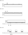
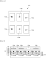
- FIG. 1 is a sectional view of a display apparatus according to a first exemplary embodiment of the present disclosure
- FIG. 2 is a perspective view of a light emitting part of the display apparatus according to the first exemplary embodiment of the present disclosure.
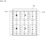
- a display apparatus 100 includes a light emitting diode part 110, a TFT panel unit 130, and an anisotropic conductive film 150.
- the light emitting diode part 110 includes light emitting diodes 112, a support substrate 114, transparent electrodes 116, a blocking part 118, an insulation layer 120, and first connection electrodes 122.
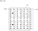
- the light emitting diode part 110 includes a plurality of light emitting diodes 112, and the plurality of light emitting diodes 112 is regularly arranged on the support substrate 114.
- the plurality of light emitting diodes 112 may be arranged in a matrix form thereon, as shown in FIG. 2 .
- the plurality of light emitting diodes 112 includes a plurality of blue light emitting diodes 112a emitting blue light, a plurality of green light emitting diodes 112b emitting green light, and a plurality of red light emitting diodes 112c emitting red light.
- the plural blue light emitting diodes 112a, the plural green light emitting diodes 112b and the plural red light emitting diodes 112c are alternately arranged such that the blue light emitting diode 112a, the green light emitting diode 112b and the red light emitting diode 112c are adjacent to one another.
- the light emitting diode part 110 allows the display apparatus 100 to be driven by power applied from an exterior power source. That is, an image can be reproduced through on-off combination of the light emitting diodes 112 in the light emitting diode part 110 without using a separate LCD. Accordingly, a region including a single light emitting diode 112 may be used as a sub-pixel in the display apparatus 100. As shown in FIG. 2 , in the light emitting diode part 110, one sub-pixel may have a larger size than the light emitting diode 112 disposed inside the sub-pixel.
- each of the light emitting diodes 112 may include an n-type semiconductor layer 23, an active layer 25, a p-type semiconductor layer 27, an n-type electrode 31, a p-type electrode 33, and a wall 35.
- the n-type semiconductor layer 23, the active layer 25 and the p-type semiconductor layer 27 may include Group III-V based compound semiconductors.
- the n-type semiconductor layer 23, the active layer 25 and the p-type semiconductor layer 27 may include nitride semiconductors such as (Al, Ga, In)N.
- locations of the n-type semiconductor layer 23 and the p-type semiconductor layer 27 can be interchanged.
- the n-type semiconductor layer 23 may include an n-type dopant (for example, Si) and the p-type semiconductor layer 27 may include a p-type dopant (for example, Mg).
- the active layer 25 is interposed between the n-type semiconductor layer 23 and the p-type semiconductor layer 27.
- the active layer 25 may have a multi-quantum well (MQW) structure and a composition of the active layer 25 may be determined so as to emit light having a desired peak wavelength.
- MQW multi-quantum well
- the light emitting structure including the n-type semiconductor layer 23, the active layer 25 and the p-type semiconductor layer 27 may be formed similar to a vertical type light emitting diode 112.
- the n-type electrode 31 may be formed on an outer surface of the n-type semiconductor layer 23 and the p-type electrode 33 may be formed on an outer surface of the p-type semiconductor layer 27.
- a bonding portion S may be formed between the p-type electrode 33 and the transparent electrode 116, and the wall 35 may be formed to prevent the bonding portion S from escaping from a space between the p-type electrode 33 and the transparent electrode 116.
- the wall 35 may be formed to cover a portion of the p-type electrode 33 such that the p-type electrode 33 can be exposed on the p-type semiconductor layer 27, and may be composed of a plurality of layers, as shown in the drawings.
- the wall 35 may include a first layer and a second layer, and may be formed by forming the first layer including SiN on the p-type semiconductor layer 27 so as to cover a portion of the p-type electrode 33, followed by forming the second layer including SiO 2 on the first layer.
- the second layer may have a greater thickness and a smaller width than the first layer.
- the support substrate 114 is a substrate on which the plurality of light emitting diodes 112 will be mounted, and may be an insulation substrate, a conductive substrate, or a circuit board.
- the support substrate 114 may be a sapphire substrate, a gallium nitride substrate, a glass substrate, a silicon carbide substrate, a silicon substrate, a metal substrate, or a ceramic substrate.
- the support substrate 114 is formed on an upper surface thereof with the plurality of conductive patterns 35 to be electrically connected to the plurality of light emitting diodes 112 and may include a circuit pattern therein, as needed.
- the support substrate 114 may be a flexible substrate.
- the transparent electrode 116 may be formed on the support substrate 114 and may be electrically connected to the p-type electrode 33 of the light emitting diode 112.
- a plurality of transparent electrodes 116 may be formed on the support substrate 114, and one light emitting diode 112 may be coupled to one transparent electrode 116, or the plurality of light emitting diodes 112 may be coupled to one transparent electrode 116, as needed.
- the plural transparent electrodes 116 may be separated from each other on the support substrate 114.
- the transparent electrodes 116 may be formed of indium tin oxide (ITO) and the like.
- the blocking part 118 is formed on the support substrate 114 and is provided in plural.
- the blocking part 118 allows light emitted from the light emitting diodes 112 to be emitted to the outside only through the transparent electrodes 116 and prevents light emitted from a certain light emitting diode from mixing with light emitted from adjacent light emitting diodes 112. Accordingly, the blocking part 118 may be formed between the transparent electrodes 116 separated from each other and may be formed to cover a portion of each of the transparent electrodes 116, as needed.
- the blocking part 118 is formed of chromium (Cr).
- the insulation layer 120 surrounds each of the light emitting diodes 112 and covers an exposed surface of a connecting plane between the light emitting diodes 112. With this structure, the insulation layer 120 may be formed to partially cover the blocking part 118. In the structure wherein the insulation layer 120 surrounds each of the light emitting diodes 112, the n-type semiconductor layer 23 and the n-type electrode 31 of each of the light emitting diodes 112 can be exposed through the insulation layer 120.
- the first connection electrodes 122 cover the insulation layer 120 and may also cover the n-type semiconductor layer 23 and the n-type electrode 31 not covered by the insulation layer 120. Accordingly, the first connection electrodes 122 may be electrically connected to the n-type semiconductor layer 23.
- the TFT panel unit 130 includes a panel substrate 132 and second connection electrodes 134 and is coupled to the light emitting diode part 110 to supply power to the light emitting diode part 110.
- the TFT panel unit 130 controls power supplied to the light emitting diode part 110 to allow only some of the light emitting diodes 112 in the light emitting diode part 110 to emit light.
- the panel substrate 132 has a TFT drive circuit therein.
- the TFT drive circuit may be a circuit for driving an active matrix (AM) or a circuit for driving a passive matrix (PM).
- the second connection electrode 134 may be electrically connected to the TFT drive circuit of the panel substrate 132 and to the first connection electrode 122 of the light emitting diode part 110.
- power supplied through the TFT drive circuit can be supplied to each of the light emitting diodes 112 through the first and second connection electrodes 122, 134.
- the second connection electrode 134 may be covered by a separate protective layer, which may include SiNx.
- the anisotropic conductive film 150 serves to electrically connect the light emitting diode part 110 to the TFT panel unit 130.
- the anisotropic conductive film 150 includes an adhesive organic insulation material and contains conductive particles uniformly dispersed therein to achieve electrical connection.
- the anisotropic conductive film 150 exhibits conductivity in the thickness direction thereof and insulation properties in the plane direction thereof.
- the anisotropic conductive film exhibits adhesive properties and can be used to bond the light emitting diode part 110 to the TFT panel such that the light emitting diode part 110 can be electrically connected to the TFT panel therethrough.
- the anisotropic conductive film 150 can be advantageously used to connect ITO electrodes which are difficult to solder at high temperature.
- the first connection electrode 122 of the light emitting diode part 110 is electrically connected to the second connection electrode 134 of the TFT panel unit 130, thereby forming an electrode connection portion 152.
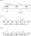
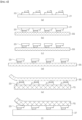
- FIG. 3 and FIG. 4 are sectional views and plan views illustrating a process of forming the light emitting diode part 110 of the display apparatus 100 according to the first exemplary embodiment of the present disclosure.
- an n-type semiconductor layer 23, an active layer 25 and a p-type semiconductor layer 27 are sequentially grown on a growth substrate.
- a p-type electrode 33 is formed on the p-type semiconductor layer 27.
- a plurality of p-type electrodes 33 may be formed to be separated from each other by a predetermined distance such that one p-type electrode 33 is provided to one light emitting diode 112.
- a wall 35 is formed on the p-type semiconductor layer 27.
- the wall 35 may be composed of first and second layers.
- the first layer includes SiN and is formed to cover the entirety of the p-type semiconductor layer 27 while covering a portion of each of the p-type electrodes 33.
- the second layer includes SiO 2 and is formed on the first layer.
- the second layer may have a greater thickness than the first layer and may be formed on a region of the first layer in which the p-type electrode 33 is not formed.
- the grown semiconductor layers are coupled to a first substrate.
- the second layer of the wall 35 is coupled to the first substrate.
- the first substrate may be the same as the support substrate 114 and may be a sapphire substrate in this exemplary embodiment.
- the growth substrate may be removed from the semiconductor layers by LLO and the semiconductor layers may be divided into individual light emitting diodes 112 by etching.
- division of the semiconductor layers into individual light emitting diodes 112 may be performed by dry etching.
- n-type electrodes 31 may be formed on the n-type semiconductor layer 23. Alternatively, the n-type electrodes 31 may be formed before division of the semiconductor layers into the individual light emitting diodes 112. Then, as shown in FIG. 3F , the light emitting diodes 112 are coupled to a second substrate such that the n-type electrodes 31 can be coupled to the second substrate, followed by removing the first substrate.
- the second substrate may be the same kind of substrate as the first substrate.
- the light emitting diodes 112 are coupled to a third substrate such that the wall 35 can be coupled to the third substrate, followed by removing the second substrate.
- the third substrate may be a stretchable substrate that is stretchable in the plane direction thereof.
- the stretchable third substrate is stretched to enlarge distances between the light emitting diodes 112.
- the light emitting diodes 112 are coupled to a fourth substrate such that the n-type electrodes 31 can be coupled to the fourth substrate, as shown in FIG. 3I .
- the fourth substrate may include a flexible base and a bonding layer formed on the base.
- the plurality of light emitting diodes 112 arranged on the fourth substrate is bonded to the support substrate 114, which may be formed with a bonding portion S at a location corresponding to each of the light emitting diodes 112.
- the bonding portion S is formed at a mounting location of each of the light emitting diodes 112 on the support substrate 114. Accordingly, even when the entire plural light emitting diodes coupled to the fourth substrate are transferred to an upper surface of the support substrate 114, the light emitting diodes 112 can be transferred only to locations of the support substrate 114 at which the bonding portions S are formed.
- external force may be applied only to the light emitting diodes 112 disposed corresponding to the locations of the bonding portions S on the support substrate 114 among the light emitting diodes 112 coupled to the fourth substrate, such that only the light emitting diodes 112 disposed corresponding to the bonding portions S can be bonded to the support substrate 114.
- the light emitting diodes 112 can be coupled to the support substrate at the locations of the bonding portions S thereon.
- the stretchable third substrate may be omitted. That is, only some light emitting diodes 112 may be coupled to the support substrate 114 by selectively applying external force only to target light emitting diodes to be coupled to the support substrate 114 using a flexible fourth substrate instead of the second substrate shown in FIG. 3F .
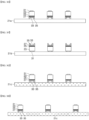
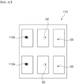
- FIG. 4A shows the bonding portions S formed on the support substrate 114, in which the bonding portions S are formed at all locations on the support substrate 114 at which the blue light emitting diodes 112a, the green light emitting diodes 112b and the red light emitting diodes 112c are coupled, respectively.
- the bonding portions S may be classified into first to third bonding portions S1, S2, S3.
- the first bonding portion S1 is formed to bond the blue light emitting diodes 112a to the support substrate and the second bonding portion S2 is formed to bond the green light emitting diodes 112b thereto.
- the third bonding portion S3 is formed to bond the red light emitting diodes 112c thereto.
- the first to third bonding portions S1, S2, S3 may have different bonding temperatures. Specifically, the first bonding portion S1 has the highest bonding temperature and the third bonding portion S3 has the lowest bonding temperature.
- the first bonding portion S1 is formed of AgSn and has a bonding temperature of about 230°C and the second bonding portion S2 is formed of ZnSn and has a bonding temperature of about 198°C.
- the third bonding portion S3 is formed of In and has a bonding temperature of about 157°C.
- the bonding temperatures of the first to third bonding portions S1, S2, S3 are differently set due to different bonding sequences of the light emitting diodes 112 to the respective bonding portions S.
- the first bonding portion S1 Since the blue light emitting diodes 112a are first bonded to the support substrate 114, the first bonding portion S1 has the highest bonding temperature. Thus, since the first bonding portion S1 has a higher bonding temperature than the second bonding portion S2 or the third bonding portion S3, the first bonding portion S1 can maintain a bonded state of the blue light emitting diodes 112a during bonding of the green light emitting diodes 112b or the red light emitting diodes 112c.
- the fourth substrate on which the blue light emitting diodes 112a are formed is placed at a corresponding location on the support substrate 114, and the blue light emitting diodes 112a are coupled to the support substrate 114, as shown in FIG. 4B .
- the distances between the blue light emitting diodes 112a formed on the fourth substrate are widened by the stretchable substrate, which is provided as the third substrate, as compared with the distances between the blue light emitting diodes 112a formed on the growth substrate.
- each of the blue light emitting diodes 112a is not disposed at a location corresponding to the second bonding portion S2 or the third bonding portion S3. Then, with the blue light emitting diodes 112a contacting the first bonding portion S1, the first bonding portion S1 is heated to about 230°C and cooled to bond the blue light emitting diodes 112a to the support substrate 114 via the first bonding portion S1.
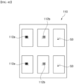
- FIG. 4C shows the blue light emitting diodes 112a bonded to the support substrate 114.
- the fourth substrate on which the green light emitting diodes 112b are formed is placed at a corresponding location on the support substrate 114, and the green light emitting diodes 112b are bonded to the support substrate 114, as shown in FIG. 4D .
- the distances between the green light emitting diodes 112b formed on the fourth substrate are greater than the distances between the green light emitting diodes 112b formed on the growth substrate, as described above.
- FIG. 4E shows the blue light emitting diodes 112a and the green light emitting diodes 112b bonded to the support substrate 114.
- the fourth substrate on which the red light emitting diodes 112c are formed is placed at a corresponding location on the support substrate 114, and the red light emitting diodes 112c are bonded to the support substrate 114, as shown in FIG. 4F .
- the distances between the red light emitting diodes 112c formed on the fourth substrate are greater than the distances between the red light emitting diodes 112c formed on the growth substrate, as described above, thereby preventing interference with the blue light emitting diodes 112a or the green light emitting diodes 112b disposed on the support substrate 114.
- FIG. 4G shows the blue light emitting diode 112a, the green light emitting diode 112b and the red light emitting diode 112c bonded to the support substrate 114.
- separation distances between the blue light emitting diode 112a, the green light emitting diode 112b and the red light emitting diode 112c formed on the different fourth substrates may be at least twice the width of each of the light emitting diodes 112. In this way, with the distances between the light emitting diodes maintained at at least twice the width of each of the light emitting diodes on the support substrate 114, the light emitting diodes 112 are bonded to the support substrate 114, thereby preventing interference between the other light emitting diodes 112.
- FIG. 3M is a sectional view corresponding to the plan view shown in FIG. 4G . That is, referring to FIG. 3M , each of the blue light emitting diodes 112a, the green light emitting diodes 112b and the red light emitting diodes 112c is bonded to the support substrate 114. In this state, an insulation layer 120 may be formed to cover the entirety of each of the light emitting diodes 112 excluding a portion thereof, as shown in FIG. 3N . The insulation layer 120 is formed to cover both the transparent electrodes 116 and the blocking part 118 while surrounding each of the light emitting diodes 112.
- the insulation layer 120 can prevent the transparent electrode 116 electrically connected to each of the light emitting diodes 112 from being exposed to the outside.
- An upper surface of the n-type semiconductor layer 23 and the n-type electrode 31 of each of the light emitting diodes 112 can be exposed through an upper surface of the insulation layer 120.
- first connection electrodes 122 may be formed on the upper surface of the insulation layer 120 to cover the n-type semiconductor layer 23 and the n-type electrodes 31, as shown in FIG. 3O .
- the light emitting diode part 110 according to this exemplary embodiment can be formed.
- the light emitting diode part 110 is bonded to the TFT panel unit 130 via an anisotropic connection film, as shown in FIG. 3P , thereby providing the display apparatus 100 according to the first exemplary embodiment, as shown in FIG. 1 .
- FIG. 5 is a sectional view of a display apparatus according to a second exemplary embodiment of the present disclosure.
- a display apparatus 100 includes a light emitting diode part 110, a TFT panel unit 130, and an anisotropic conductive film 150. Description of the same components as those of the first exemplary embodiment will be omitted.
- the light emitting diode part 110 includes light emitting diodes 112, transparent electrodes 116, a blocking part 118, an insulation layer 120, first connection electrodes 122, a transparent substrate 124, a phosphor layer 126, and a protective substrate 128.
- the light emitting diode part 110 includes a plurality of light emitting diodes 112, and blue light emitting diodes 112a emitting blue light may be used as the light emitting diodes 112.
- the blue light emitting diodes 112a are electrically connected to the transparent electrodes 116 and the blocking part 118 may be formed between the transparent electrodes 116.
- the transparent substrate 124 may be formed on the transparent electrode 116.
- the transparent substrate 124 may serve as the support substrate 114 of the display apparatus 100 according to the first exemplary embodiment.
- the support substrate 114 may be removed therefrom and the transparent substrate 124 may be formed again.
- the phosphor layer 126 may be formed on an upper surface of the transparent substrate 124.
- the phosphor layer 126 may be formed on the blue light emitting diodes 112a such that one of a green phosphor layer 126b, a red phosphor layer 126c and a transparent layer 126e is formed thereon.
- a blocking layer 126d may be formed between the green phosphor layer 126b, the red phosphor layer 126c and the transparent layer 126e.
- the green phosphor layer 126b converts wavelengths of light emitted from the blue light emitting diode 112a such that green light can be emitted from the green phosphor layer 126b
- the red phosphor layer 126c converts wavelengths of light emitted from the blue light emitting diode 112a such that red light can be emitted from the red phosphor layer 126c.
- the transparent layer 126e is placed near the green phosphor layer 126b and the red phosphor layer 126c to allow blue light emitted from the blue light emitting diode 112a to pass therethrough. Accordingly, red light, green light and blue light can be emitted through the phosphor layer 126.
- the protective substrate 128 may be formed on an upper surface of the phosphor layer 126.
- the protective substrate 128 can prevent the phosphor layer 126 from being exposed to the outside and may be formed of a transparent material as in the transparent substrate 124.
- FIG. 6 is a sectional view of a display apparatus according to a third exemplary embodiment of the present disclosure.
- a display apparatus 100 includes a light emitting diode part 110, a TFT panel unit 130, and an anisotropic conductive film 150. Description of the same components as those of the first exemplary embodiment will be omitted.
- the light emitting diode part 110 includes light emitting diodes 112, transparent electrodes 116, a blocking part 118, a white phosphor film 125, and a color film.
- the light emitting diode part 110 includes a plurality of light emitting diodes 112, and blue light emitting diodes 112a are used as in the second exemplary embodiment.
- the blue light emitting diodes 112a are electrically connected to the transparent electrodes 116 and the blocking part 118 may be formed between the transparent electrodes 116.
- the white phosphor film 125 may be formed on an upper surface of the transparent electrode 116.
- the white phosphor film 125 converts blue light emitted from the blue light emitting diode 112a into white light.
- the white phosphor film 125 may include a green phosphor and a red phosphor.
- the color filter 127 may be formed on an upper surface of the white phosphor film 125.
- the color filter 127 may be formed in a film shape and filters white light emitted from the white phosphor film 125 excluding one of blue light, green light and red light of the white light.
- the color filter 127 may include a blue light portion 127a that filters white light to allow blue light to pass therethrough, a green light portion 127b that filters white light to allow green light to pass therethrough, and a red light portion 127c that filters white light to allow red light to pass therethrough.
- the color filter 127 may further include a transparent portion 127e to allow white light to pass therethrough without wavelength conversion.
- the blue light portion 127a, the green light portion 127b, the red light portion 127c and the transparent portion 127e may be disposed adjacent one another.
- a light blocking portion 127d may be formed between the blue light portion 127a, the green light portion 127b, the red light portion 127c and the transparent portion 127e.
- FIG. 7 is a sectional view of a display apparatus according to a fourth exemplary embodiment of the present disclosure.
- a display apparatus 100 includes a light emitting diode part 110, a TFT panel unit 130, and an anisotropic conductive film 150. Description of the same components as those of the first and third exemplary embodiments will be omitted.
- the light emitting diode part 110 includes light emitting diodes 112, transparent electrodes 116, a blocking part 118, a transparent substrate 124, a white phosphor film 125, and a color film.
- the light emitting diode part 110 includes a plurality of light emitting diodes 112, and blue light emitting diodes 112a are used as in the second exemplary embodiment.
- the blue light emitting diodes 112a are electrically connected to the transparent electrodes 116 and the blocking part 118 may be formed between the transparent electrodes 116.
- the transparent substrate 124 may be formed on an upper surface of the transparent electrode 116.
- the transparent substrate 124 may serve as the support substrate 114 of the display apparatus 100 according to the first exemplary embodiment.
- the support substrate 114 may be removed therefrom and the transparent substrate 124 may be formed again.
- the white phosphor film 125 may be formed on an upper surface of the transparent electrode 116 and the color filter 127 may be formed on an upper surface of the white phosphor film 125.
- the white phosphor film 125 and the color filter 127 are the same as those of the display apparatus according to the third exemplary embodiment and detailed descriptions thereof will be omitted.
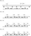
- FIG. 8 shows sectional views of a display apparatus according to a fifth exemplary embodiment of the present disclosure.
- FIG. 8(a) to FIG. 8(f) are sectional views illustrating a process of manufacturing the display apparatus according to the fifth exemplary embodiment, in which a plurality of light emitting structures grown on a growth substrate is coupled to a support substrate after adjustment of separation distances between the light emitting structures using a stretchable sheet SS.
- the display apparatus includes light emitting structures 23, n-type bumps 31, p-type bumps 33, a support substrate 37, and a wavelength conversion part 43. Description of the same components as those of the above exemplary embodiments will be omitted. The following description will focus on a process of coupling light emitting structures 23 grown on the growth substrate 21 to the support substrate 37 with reference to FIG. 8 .
- the light emitting structure 23 may include a partially exposed region of the n-type semiconductor layer 25, which is formed by partially removing the p-type semiconductor layer 29 and the active layer 27.
- An n-type electrode pad may be placed on the exposed region of the n-type semiconductor layer 25 and a p-type electrode pad may be placed on the p-type semiconductor layer 29.
- the light emitting structure 23 uses a flip-chip type light emitting diode in this exemplary embodiment, it should be understood that a vertical type light emitting diode or a lateral type light emitting diode may also be used.
- the growth substrate 21 may be selected from among any substrates allowing growth of nitride semiconductor layers thereon and may be an insulation or conductive substrate.
- the growth substrate 21 may be a sapphire substrate, a silicon substrate, a silicon carbide substrate, an aluminum nitride substrate, or a gallium nitride substrate.
- the growth substrate 21 may be a sapphire substrate and may include a C-plane as a growth plane on which nitride semiconductor layers are grown.
- the plurality of light emitting structures 23 is grown on the growth substrate 21.
- the plural light emitting structures 23 are arranged in a predetermined pattern on the growth substrate 21 and are separated from each other during growth.
- the light emitting structures 23 grown on the growth substrate 21 are coupled to an upper surface of the stretchable sheet, as shown in FIG. 8(b) .
- the growth substrate 21 is removed from the light emitting structures by LLO and the like, as shown in FIG. 8(c) .
- FIG. 8(d) shows one example in which the separation distances between the light emitting structures 23 are enlarged by stretching the stretchable sheet (SS).
- the stretchable sheet (SS) may be a blue sheet.
- the stretchable sheet (SS) is turned upside down in a stretched state and coupled to a fixing sheet (FS) via the light emitting structures 23 such that the light emitting structures 23 are coupled to the fixing sheet.
- This state is shown in FIG. 8(e) , and after the plurality of light emitting structures 23 is coupled to the fixing sheet (FS), the stretchable sheet (SS) is removed from the upper surfaces of the plurality of light emitting structures 23.
- the stretchable sheet (SS) can be uniformly stretchable in two dimensions, the distances between the plural light emitting structures 23 can be uniformly widened. The distances between the plural light emitting structures 23 can be adjusted in various ways as needed.
- the fixing sheet (FS) serves to fix the locations of the light emitting structure 23 in order to maintain the distances between the plural light emitting structures 23 adjusted by the stretchable sheet (SS).
- the support substrate 37 includes conductive patterns 35 or interconnection circuits, and may be a general PCB, a flexible substrate, or a stretchable substrate like the stretchable sheet (SS).
- the separation distances between the plural light emitting structures 23 may be adjusted using the stretchable sheet (SS), the light emitting structures 23 may be simultaneously transferred to the support substrate after uniformly increasing the distances therebetween. Accordingly, the plurality of light emitting structures 23 used in the display apparatus according to the present disclosure may also be used not only in a small wearable apparatus, but also in a large display.
- display apparatus 110 light emitting diode part 112: light emitting diode 112a: blue light emitting diode 112b: green light emitting diode 112c: red light emitting diode 23: n-type semiconductor layer 25: active layer 27: p-type semiconductor layer 31: n-type electrode 33: p-type electrode 35: wall 114: support substrate 116: transparent electrode 118: blocking portion 120: insulation layer 122: first connection electrode 124: transparent substrate 125: white phosphor film 126: phosphor layer 126b: green phosphor layer 126c: red phosphor layer 126d: blocking layer 126e: transparent layer 127: color filter 127a: blue light portion 127b: green light portion 127c: red light portion 127d: light blocking portion 127e: transparent portion 128: protective substrate 130: TFT panel unit 132: panel substrate 134: second connection electrode 150: anisotropic conductive film 152: electrode connection portion 200:
Landscapes
- Engineering & Computer Science (AREA)
- Manufacturing & Machinery (AREA)
- Physics & Mathematics (AREA)
- General Physics & Mathematics (AREA)
- Theoretical Computer Science (AREA)
- Led Device Packages (AREA)
- Devices For Indicating Variable Information By Combining Individual Elements (AREA)
- Led Devices (AREA)
- Computer Hardware Design (AREA)
Abstract
Description
- Exemplary embodiments of the present disclosure relate to a display apparatus and a method of manufacturing the same, and more particularly, to a display apparatus using micro-light emitting diodes and a method of manufacturing the same.
- A light emitting diode refers to an inorganic semiconductor device configured to emit light through recombination of electrons and holes and has been used in various fields including displays, automobile lamps, general lighting, and the like. Since the light emitting diode has various advantages such as long lifespan, low power consumption, and rapid response, it is expected that a light emitting device using the light emitting diode will replace existing light sources.
- Recently, smart TVs or monitors realize colors using a thin film transistor liquid crystal display (TFT LCD) panel and tend to use light emitting diodes (LEDs) as a light source for a backlight unit for color realization. In addition, a display apparatus is often manufactured using organic light emitting diodes (OLEDs). However, for a TFT-LCD, since one LED is used as a light source for many pixels, a light source of a backlight unit is always turned on. Accordingly, the TFT-LCD suffers from constant power consumption regardless of brightness on a displayed screen. In order to compensate for this problem, some display apparatuses are configured to divide a screen into several regions so as to allow control of brightness in these regions. However, since several to dozens of thousands of pixels are used as a unit for division of the screen, it is difficult to achieve accurate regulation of brightness while reducing power consumption. On the other hand, although an OLED has continuously reduced power consumption through development of technology, the OLED still has much higher power consumption than LEDs formed of inorganic semiconductors and thus has low efficiency.
- In addition, a PM drive type OLED can suffer from deterioration in response speed upon pulse amplitude modulation (PAM) of the OLED having large capacitance, and can suffer from deterioration in lifespan upon high current driving through pulse width modulation (PWM) for realizing a low duty ratio. Moreover, an AM driving type OLED requires connection of TFTs for each pixel, thereby causing increase in manufacturing costs and non-uniform brightness according to characteristics of TFTs.
-
Japanese Patent Laid-open Publication No. 2015-500562 (January 5, 2015 - Exemplary embodiments provide a display apparatus using micro-light emitting diodes providing low power consumption to be applicable to a wearable apparatus, a smartphone or a TV, and a method of manufacturing the same.
- Exemplary embodiments provide a display apparatus providing low power consumption and enabling accurate regulation of brightness and a method of manufacturing the same.
- In accordance with one aspect of the present disclosure, a display apparatus includes: a first substrate including a light emitting diode part including a plurality of light emitting diodes regularly arranged on the first substrate; and a second substrate including a TFT panel unit including a plurality of TFTs driving the light emitting diodes, wherein the first substrate and the second substrate are coupled to each other so as to face each other such that the light emitting diodes are electrically connected to the TFTs, respectively.
- The light emitting diode part may include: a support substrate; a plurality of blue light emitting diodes arranged on an upper surface of the support substrate; a plurality of green light emitting diodes arranged on the upper surface of the support substrate to be placed adjacent the plurality of blue light emitting diodes; and a plurality of red light emitting diodes arranged on the upper surface of the support substrate to be placed adjacent either the plurality of blue light emitting diodes or the plurality of green light emitting diodes.
- Each of the plurality of blue light emitting diodes, the plurality of green light emitting diodes and the plurality of red light emitting diodes may include an n-type semiconductor layer; a p-type semiconductor layer; an active layer interposed between the n-type semiconductor layer and the p-type semiconductor layer; an n-type electrode coupled to the n-type semiconductor layer; a p-type electrode coupled to the p-type semiconductor layer; and a wall surrounding the p-type electrode.
- The light emitting diode part may further include a first bonding portion bonding the plurality of blue light emitting diodes to the support substrate; a second bonding portion bonding the plurality of green light emitting diodes to the support substrate; and a third bonding portion bonding the plurality of red light emitting diodes to the support substrate, and the first to third bonding portions may have different melting points.
- The display apparatus may further include an anisotropic conductive film electrically connecting the light emitting diode part to the TFT panel unit.
- The plurality of light emitting diodes may include blue light emitting diodes emitting blue light, and the display apparatus may further include a wavelength conversion part including at least one of a blue light portion emitting the blue light, a green light portion emitting green light through conversion of the blue light into the green light, and a red light portion emitting red light through conversion of the blue light into the red light.
- The plurality of light emitting diodes may include blue light emitting diodes emitting blue light and red light emitting diodes emitting red light, and the display apparatus may further include a wavelength conversion part including at least one of a blue light portion emitting the blue light, a green light portion emitting green light through conversion of the blue light into the green light, and a red light portion emitting the red light.
- The wavelength conversion part may be formed on a third substrate and the first substrate may be coupled to the third substrate to allow wavelength conversion of light emitted from the plurality of light emitting diodes. The green light portion and the red light portion may include phosphors. Specifically, the green light portion may include nitride phosphors and the red light portion may include nitride or fluoride phosphors (KSF).
- At least one of the first to third substrates may be a transparent substrate or an opaque flexible substrate.
- The plurality of light emitting diodes may include blue light emitting diodes emitting blue light, and the display apparatus may further include a white phosphor portion converting blue light emitted from the blue light emitting diodes into white light; and a color filter including a blue light portion allowing blue light of the white light emitted through the white phosphor portion to pass therethrough, a green light portion allowing green light of the white light emitted through the white phosphor portion to pass therethrough, and a red light portion allowing red light of the white light emitted through the white phosphor portion to pass therethrough.
- Each of the light emitting diodes may include an n-type semiconductor layer, a p-type semiconductor layer, and an active layer interposed between the n-type semiconductor layer and the p-type semiconductor layer, and a wall may be formed on the p-type semiconductor layer.
- In accordance with a further aspect of the present disclosure, a method of manufacturing a display apparatus includes: forming a light emitting diode part such that a plurality of light emitting diodes is regularly arranged therein; and coupling the light emitting diode part to a TFT panel unit, wherein forming the light emitting diode part may include forming the plurality of light emitting diodes on a substrate to be regularly arranged thereon; transferring the plurality of light emitting diodes to a stretchable substrate; two-dimensionally enlarging the stretchable substrate such that a separation distance between the light emitting diodes is enlarged; and coupling at least one of the light emitting diodes to a support substrate, with the separation distance between the light emitting diodes enlarged by the stretchable substrate.
- The separation distance between the light emitting diodes enlarged by the stretchable substrate may be twice a width of the light emitting diodes.
- Coupling the light emitting diode part to the TFT panel unit may be performed using an anisotropic conductive film.
- According to exemplary embodiments, the display apparatus employs micro-light emitting diodes formed of nitride semiconductors and thus can provide high efficiency and high resolution to be applicable to a wearable apparatus while reducing power consumption.
- Further, the display apparatus according to the exemplary embodiments employs a stretchable substrate, thereby providing more convenience in manufacture of the display apparatus than manufacture of the display apparatus using micro-light emitting diodes.
-
-
FIG. 1 is a sectional view of a display apparatus according to a first exemplary embodiment of the present disclosure. -
FIG. 2 is a perspective view of a light emitting part of the display apparatus according to the first exemplary embodiment of the present disclosure. -
FIG. 3 andFIG. 4 are sectional views and plan views illustrating a process of forming the light emitting diode part of the display apparatus according to the first exemplary embodiment of the present disclosure. -
FIG. 5 is a sectional view of a display apparatus according to a second exemplary embodiment of the present disclosure. -
FIG. 6 is a sectional view of a display apparatus according to a third exemplary embodiment of the present disclosure. -
FIG. 7 is a sectional view of a display apparatus according to a fourth exemplary embodiment of the present disclosure. -
FIG. 8 shows sectional views of a display apparatus according to a fifth exemplary embodiment of the present disclosure. - Hereinafter, exemplary embodiments of the present disclosure will be described in detail with reference to the accompanying drawings.
-
FIG. 1 is a sectional view of a display apparatus according to a first exemplary embodiment of the present disclosure, andFIG. 2 is a perspective view of a light emitting part of the display apparatus according to the first exemplary embodiment of the present disclosure. - Referring to
FIG. 1 , adisplay apparatus 100 according to the first exemplary embodiment includes a lightemitting diode part 110, aTFT panel unit 130, and an anisotropicconductive film 150. - Referring to
FIG. 1 and FIG. 2 , the lightemitting diode part 110 includeslight emitting diodes 112, asupport substrate 114,transparent electrodes 116, a blockingpart 118, aninsulation layer 120, andfirst connection electrodes 122. - The light
emitting diode part 110 includes a plurality oflight emitting diodes 112, and the plurality oflight emitting diodes 112 is regularly arranged on thesupport substrate 114. For example, the plurality oflight emitting diodes 112 may be arranged in a matrix form thereon, as shown inFIG. 2 . In this exemplary embodiment, the plurality oflight emitting diodes 112 includes a plurality of bluelight emitting diodes 112a emitting blue light, a plurality of greenlight emitting diodes 112b emitting green light, and a plurality of redlight emitting diodes 112c emitting red light. The plural bluelight emitting diodes 112a, the plural greenlight emitting diodes 112b and the plural redlight emitting diodes 112c are alternately arranged such that the bluelight emitting diode 112a, the greenlight emitting diode 112b and the redlight emitting diode 112c are adjacent to one another. - In this exemplary embodiment, as shown in
FIG. 2 , the lightemitting diode part 110 allows thedisplay apparatus 100 to be driven by power applied from an exterior power source. That is, an image can be reproduced through on-off combination of thelight emitting diodes 112 in the lightemitting diode part 110 without using a separate LCD. Accordingly, a region including a singlelight emitting diode 112 may be used as a sub-pixel in thedisplay apparatus 100. As shown inFIG. 2 , in the lightemitting diode part 110, one sub-pixel may have a larger size than thelight emitting diode 112 disposed inside the sub-pixel. - Referring to
FIG. 1 again, each of thelight emitting diodes 112 may include an n-type semiconductor layer 23, anactive layer 25, a p-type semiconductor layer 27, an n-type electrode 31, a p-type electrode 33, and awall 35. The n-type semiconductor layer 23, theactive layer 25 and the p-type semiconductor layer 27 may include Group III-V based compound semiconductors. By way of example, the n-type semiconductor layer 23, theactive layer 25 and the p-type semiconductor layer 27 may include nitride semiconductors such as (Al, Ga, In)N. In other exemplary embodiments, locations of the n-type semiconductor layer 23 and the p-type semiconductor layer 27 can be interchanged. - The n-
type semiconductor layer 23 may include an n-type dopant (for example, Si) and the p-type semiconductor layer 27 may include a p-type dopant (for example, Mg). Theactive layer 25 is interposed between the n-type semiconductor layer 23 and the p-type semiconductor layer 27. Theactive layer 25 may have a multi-quantum well (MQW) structure and a composition of theactive layer 25 may be determined so as to emit light having a desired peak wavelength. - In addition, the light emitting structure including the n-
type semiconductor layer 23, theactive layer 25 and the p-type semiconductor layer 27 may be formed similar to a vertical typelight emitting diode 112. In this structure, the n-type electrode 31 may be formed on an outer surface of the n-type semiconductor layer 23 and the p-type electrode 33 may be formed on an outer surface of the p-type semiconductor layer 27. - Further, as shown in
FIG. 1 , in order to couple each of thelight emitting diodes 112 similar to the vertical type light emitting diode to thetransparent electrode 116 of thesupport substrate 114, a bonding portion S may be formed between the p-type electrode 33 and thetransparent electrode 116, and thewall 35 may be formed to prevent the bonding portion S from escaping from a space between the p-type electrode 33 and thetransparent electrode 116. - The
wall 35 may be formed to cover a portion of the p-type electrode 33 such that the p-type electrode 33 can be exposed on the p-type semiconductor layer 27, and may be composed of a plurality of layers, as shown in the drawings. Thewall 35 may include a first layer and a second layer, and may be formed by forming the first layer including SiN on the p-type semiconductor layer 27 so as to cover a portion of the p-type electrode 33, followed by forming the second layer including SiO2 on the first layer. The second layer may have a greater thickness and a smaller width than the first layer. - The
support substrate 114 is a substrate on which the plurality oflight emitting diodes 112 will be mounted, and may be an insulation substrate, a conductive substrate, or a circuit board. By way of example, thesupport substrate 114 may be a sapphire substrate, a gallium nitride substrate, a glass substrate, a silicon carbide substrate, a silicon substrate, a metal substrate, or a ceramic substrate. Thesupport substrate 114 is formed on an upper surface thereof with the plurality ofconductive patterns 35 to be electrically connected to the plurality oflight emitting diodes 112 and may include a circuit pattern therein, as needed. Thesupport substrate 114 may be a flexible substrate. - The
transparent electrode 116 may be formed on thesupport substrate 114 and may be electrically connected to the p-type electrode 33 of thelight emitting diode 112. In this exemplary embodiment, a plurality oftransparent electrodes 116 may be formed on thesupport substrate 114, and onelight emitting diode 112 may be coupled to onetransparent electrode 116, or the plurality oflight emitting diodes 112 may be coupled to onetransparent electrode 116, as needed. In addition, the pluraltransparent electrodes 116 may be separated from each other on thesupport substrate 114. By way of example, thetransparent electrodes 116 may be formed of indium tin oxide (ITO) and the like. - The blocking
part 118 is formed on thesupport substrate 114 and is provided in plural. The blockingpart 118 allows light emitted from thelight emitting diodes 112 to be emitted to the outside only through thetransparent electrodes 116 and prevents light emitted from a certain light emitting diode from mixing with light emitted from adjacentlight emitting diodes 112. Accordingly, the blockingpart 118 may be formed between thetransparent electrodes 116 separated from each other and may be formed to cover a portion of each of thetransparent electrodes 116, as needed. In this exemplary embodiment, the blockingpart 118 is formed of chromium (Cr). - The
insulation layer 120 surrounds each of thelight emitting diodes 112 and covers an exposed surface of a connecting plane between thelight emitting diodes 112. With this structure, theinsulation layer 120 may be formed to partially cover the blockingpart 118. In the structure wherein theinsulation layer 120 surrounds each of thelight emitting diodes 112, the n-type semiconductor layer 23 and the n-type electrode 31 of each of thelight emitting diodes 112 can be exposed through theinsulation layer 120. - The
first connection electrodes 122 cover theinsulation layer 120 and may also cover the n-type semiconductor layer 23 and the n-type electrode 31 not covered by theinsulation layer 120. Accordingly, thefirst connection electrodes 122 may be electrically connected to the n-type semiconductor layer 23. - The
TFT panel unit 130 includes apanel substrate 132 andsecond connection electrodes 134 and is coupled to the light emittingdiode part 110 to supply power to the light emittingdiode part 110. TheTFT panel unit 130 controls power supplied to the light emittingdiode part 110 to allow only some of thelight emitting diodes 112 in the light emittingdiode part 110 to emit light. - The
panel substrate 132 has a TFT drive circuit therein. The TFT drive circuit may be a circuit for driving an active matrix (AM) or a circuit for driving a passive matrix (PM). - The
second connection electrode 134 may be electrically connected to the TFT drive circuit of thepanel substrate 132 and to thefirst connection electrode 122 of the light emittingdiode part 110. In this structure, power supplied through the TFT drive circuit can be supplied to each of thelight emitting diodes 112 through the first andsecond connection electrodes second connection electrode 134 may be covered by a separate protective layer, which may include SiNx. - The anisotropic
conductive film 150 serves to electrically connect the light emittingdiode part 110 to theTFT panel unit 130. The anisotropicconductive film 150 includes an adhesive organic insulation material and contains conductive particles uniformly dispersed therein to achieve electrical connection. The anisotropicconductive film 150 exhibits conductivity in the thickness direction thereof and insulation properties in the plane direction thereof. In addition, the anisotropic conductive film exhibits adhesive properties and can be used to bond the light emittingdiode part 110 to the TFT panel such that the light emittingdiode part 110 can be electrically connected to the TFT panel therethrough. Particularly, the anisotropicconductive film 150 can be advantageously used to connect ITO electrodes which are difficult to solder at high temperature. - As such, in the structure wherein the light emitting
diode part 110 is coupled to the TFT panel via the anisotropicconductive film 150, thefirst connection electrode 122 of the light emittingdiode part 110 is electrically connected to thesecond connection electrode 134 of theTFT panel unit 130, thereby forming anelectrode connection portion 152. -
FIG. 3 andFIG. 4 are sectional views and plan views illustrating a process of forming the light emittingdiode part 110 of thedisplay apparatus 100 according to the first exemplary embodiment of the present disclosure. - The process of forming the light emitting
diode part 110 according to this exemplary embodiment will be described with reference toFIG. 3 andFIG. 4 . First, as shown inFIG. 3A , an n-type semiconductor layer 23, anactive layer 25 and a p-type semiconductor layer 27 are sequentially grown on a growth substrate. Then, a p-type electrode 33 is formed on the p-type semiconductor layer 27. In this exemplary embodiment, a plurality of p-type electrodes 33 may be formed to be separated from each other by a predetermined distance such that one p-type electrode 33 is provided to onelight emitting diode 112. - Referring to
FIG. 3B , after forming the p-type electrodes 33, awall 35 is formed on the p-type semiconductor layer 27. Thewall 35 may be composed of first and second layers. The first layer includes SiN and is formed to cover the entirety of the p-type semiconductor layer 27 while covering a portion of each of the p-type electrodes 33. The second layer includes SiO2 and is formed on the first layer. The second layer may have a greater thickness than the first layer and may be formed on a region of the first layer in which the p-type electrode 33 is not formed. - Referring to
FIG. 3C , after thewall 35 is formed on the p-type semiconductor layer 27, the grown semiconductor layers are coupled to a first substrate. In this process, the second layer of thewall 35 is coupled to the first substrate. The first substrate may be the same as thesupport substrate 114 and may be a sapphire substrate in this exemplary embodiment. - Referring to
FIG. 3D , with the semiconductor layers coupled to the first substrate, the growth substrate may be removed from the semiconductor layers by LLO and the semiconductor layers may be divided into individuallight emitting diodes 112 by etching. Here, division of the semiconductor layers into individuallight emitting diodes 112 may be performed by dry etching. - Referring to
FIG. 3E , after the semiconductor layers are divided into the individuallight emitting diodes 112, n-type electrodes 31 may be formed on the n-type semiconductor layer 23. Alternatively, the n-type electrodes 31 may be formed before division of the semiconductor layers into the individuallight emitting diodes 112. Then, as shown inFIG. 3F , thelight emitting diodes 112 are coupled to a second substrate such that the n-type electrodes 31 can be coupled to the second substrate, followed by removing the first substrate. The second substrate may be the same kind of substrate as the first substrate. - Then, as shown in
FIG. 3G , thelight emitting diodes 112 are coupled to a third substrate such that thewall 35 can be coupled to the third substrate, followed by removing the second substrate. In this exemplary embodiment, the third substrate may be a stretchable substrate that is stretchable in the plane direction thereof. Thus, as shown inFIG. 3H , the stretchable third substrate is stretched to enlarge distances between thelight emitting diodes 112. - With the distances between the
light emitting diodes 112 enlarged, thelight emitting diodes 112 are coupled to a fourth substrate such that the n-type electrodes 31 can be coupled to the fourth substrate, as shown inFIG. 3I . As a result, the distances between thelight emitting diodes 112 can be maintained by the stretchable third substrate. In this exemplary embodiment, the fourth substrate may include a flexible base and a bonding layer formed on the base. - Then, referring to
FIG. 3J , the plurality oflight emitting diodes 112 arranged on the fourth substrate is bonded to thesupport substrate 114, which may be formed with a bonding portion S at a location corresponding to each of thelight emitting diodes 112. With thetransparent electrodes 116 and the blockingpart 118 formed on thesupport substrate 114, the bonding portion S is formed at a mounting location of each of thelight emitting diodes 112 on thesupport substrate 114. Accordingly, even when the entire plural light emitting diodes coupled to the fourth substrate are transferred to an upper surface of thesupport substrate 114, thelight emitting diodes 112 can be transferred only to locations of thesupport substrate 114 at which the bonding portions S are formed. - Referring to
FIG. 3K , external force may be applied only to thelight emitting diodes 112 disposed corresponding to the locations of the bonding portions S on thesupport substrate 114 among thelight emitting diodes 112 coupled to the fourth substrate, such that only thelight emitting diodes 112 disposed corresponding to the bonding portions S can be bonded to thesupport substrate 114. As a result, as shown inFIG. 3L , thelight emitting diodes 112 can be coupled to the support substrate at the locations of the bonding portions S thereon. - Although not shown in the drawings, in the case where only some
light emitting diodes 112 are selectively coupled to thesupport substrate 114 by applying external force only to target light emitting diodes among the plurality oflight emitting diodes 112 arranged on the fourth substrate as shown inFIG. 3K , the stretchable third substrate may be omitted. That is, only somelight emitting diodes 112 may be coupled to thesupport substrate 114 by selectively applying external force only to target light emitting diodes to be coupled to thesupport substrate 114 using a flexible fourth substrate instead of the second substrate shown inFIG. 3F . - In this exemplary embodiment, with regard to mounting the
light emitting diodes 112 on thesupport substrate 114 as shown inFIG. 3L , the following description will be given of mounting bluelight emitting diodes 112a, greenlight emitting diodes 112b and redlight emitting diodes 112c on thesupport substrate 114 with reference toFIG. 4 . Here, the processes of manufacturing each of the bluelight emitting diodes 112a, the greenlight emitting diodes 112b and the redlight emitting diodes 112c are the same those shown inFIG. 3A to FIG. 3I . - Like
FIG. 3J ,FIG. 4A shows the bonding portions S formed on thesupport substrate 114, in which the bonding portions S are formed at all locations on thesupport substrate 114 at which the bluelight emitting diodes 112a, the greenlight emitting diodes 112b and the redlight emitting diodes 112c are coupled, respectively. The bonding portions S may be classified into first to third bonding portions S1, S2, S3. The first bonding portion S1 is formed to bond the bluelight emitting diodes 112a to the support substrate and the second bonding portion S2 is formed to bond the greenlight emitting diodes 112b thereto. The third bonding portion S3 is formed to bond the redlight emitting diodes 112c thereto. - The first to third bonding portions S1, S2, S3 may have different bonding temperatures. Specifically, the first bonding portion S1 has the highest bonding temperature and the third bonding portion S3 has the lowest bonding temperature. For example, the first bonding portion S1 is formed of AgSn and has a bonding temperature of about 230°C and the second bonding portion S2 is formed of ZnSn and has a bonding temperature of about 198°C. The third bonding portion S3 is formed of In and has a bonding temperature of about 157°C. The bonding temperatures of the first to third bonding portions S1, S2, S3 are differently set due to different bonding sequences of the
light emitting diodes 112 to the respective bonding portions S. - Since the blue
light emitting diodes 112a are first bonded to thesupport substrate 114, the first bonding portion S1 has the highest bonding temperature. Thus, since the first bonding portion S1 has a higher bonding temperature than the second bonding portion S2 or the third bonding portion S3, the first bonding portion S1 can maintain a bonded state of the bluelight emitting diodes 112a during bonding of the greenlight emitting diodes 112b or the redlight emitting diodes 112c. - After the first to third bonding portions S1, S2, S3 are formed on the
support substrate 114 as shown inFIG. 4A , the fourth substrate on which the bluelight emitting diodes 112a are formed is placed at a corresponding location on thesupport substrate 114, and the bluelight emitting diodes 112a are coupled to thesupport substrate 114, as shown inFIG. 4B . Here, the distances between the bluelight emitting diodes 112a formed on the fourth substrate are widened by the stretchable substrate, which is provided as the third substrate, as compared with the distances between the bluelight emitting diodes 112a formed on the growth substrate. Accordingly, each of the bluelight emitting diodes 112a is not disposed at a location corresponding to the second bonding portion S2 or the third bonding portion S3. Then, with the bluelight emitting diodes 112a contacting the first bonding portion S1, the first bonding portion S1 is heated to about 230°C and cooled to bond the bluelight emitting diodes 112a to thesupport substrate 114 via the first bonding portion S1. -
FIG. 4C shows the bluelight emitting diodes 112a bonded to thesupport substrate 114. Thereafter, the fourth substrate on which the greenlight emitting diodes 112b are formed is placed at a corresponding location on thesupport substrate 114, and the greenlight emitting diodes 112b are bonded to thesupport substrate 114, as shown inFIG. 4D . Here, the distances between the greenlight emitting diodes 112b formed on the fourth substrate are greater than the distances between the greenlight emitting diodes 112b formed on the growth substrate, as described above. Accordingly, there is no interference between the bluelight emitting diode 112a and the greenlight emitting diode 112b placed at locations corresponding to the second bonding portion S2 formed on thesupport substrate 114. Then, with the greenlight emitting diodes 112b contacting the second bonding portion S2, the second bonding portion S2 is heated to about 198°C and cooled to bond the greenlight emitting diodes 112b to thesupport substrate 114 via the second bonding portion S2. In this way, the greenlight emitting diodes 112b can be bonded to thesupport substrate 114. -
FIG. 4E shows the bluelight emitting diodes 112a and the greenlight emitting diodes 112b bonded to thesupport substrate 114. Thereafter, the fourth substrate on which the redlight emitting diodes 112c are formed is placed at a corresponding location on thesupport substrate 114, and the redlight emitting diodes 112c are bonded to thesupport substrate 114, as shown inFIG. 4F . Here, the distances between the redlight emitting diodes 112c formed on the fourth substrate are greater than the distances between the redlight emitting diodes 112c formed on the growth substrate, as described above, thereby preventing interference with the bluelight emitting diodes 112a or the greenlight emitting diodes 112b disposed on thesupport substrate 114. Then, with the redlight emitting diodes 112c contacting the third bonding portion S3, the third bonding portion S3 are heated to about 157°C and cooled to bond the redlight emitting diodes 112c to thesupport substrate 114 via the third bonding portion S3. In this way, the greenlight emitting diodes 112b can be bonded to thesupport substrate 114.FIG. 4G shows the bluelight emitting diode 112a, the greenlight emitting diode 112b and the redlight emitting diode 112c bonded to thesupport substrate 114. - In this exemplary embodiment, separation distances between the blue
light emitting diode 112a, the greenlight emitting diode 112b and the redlight emitting diode 112c formed on the different fourth substrates may be at least twice the width of each of thelight emitting diodes 112. In this way, with the distances between the light emitting diodes maintained at at least twice the width of each of the light emitting diodes on thesupport substrate 114, thelight emitting diodes 112 are bonded to thesupport substrate 114, thereby preventing interference between the otherlight emitting diodes 112. -
FIG. 3M is a sectional view corresponding to the plan view shown inFIG. 4G . That is, referring toFIG. 3M , each of the bluelight emitting diodes 112a, the greenlight emitting diodes 112b and the redlight emitting diodes 112c is bonded to thesupport substrate 114. In this state, aninsulation layer 120 may be formed to cover the entirety of each of thelight emitting diodes 112 excluding a portion thereof, as shown inFIG. 3N . Theinsulation layer 120 is formed to cover both thetransparent electrodes 116 and the blockingpart 118 while surrounding each of thelight emitting diodes 112. With this structure, theinsulation layer 120 can prevent thetransparent electrode 116 electrically connected to each of thelight emitting diodes 112 from being exposed to the outside. An upper surface of the n-type semiconductor layer 23 and the n-type electrode 31 of each of thelight emitting diodes 112 can be exposed through an upper surface of theinsulation layer 120. - With the n-
type semiconductor layer 23 and the n-type electrode 31 exposed through the upper surface of theinsulation layer 120,first connection electrodes 122 may be formed on the upper surface of theinsulation layer 120 to cover the n-type semiconductor layer 23 and the n-type electrodes 31, as shown inFIG. 3O . As a result, the light emittingdiode part 110 according to this exemplary embodiment can be formed. - Thereafter, the light emitting
diode part 110 is bonded to theTFT panel unit 130 via an anisotropic connection film, as shown inFIG. 3P , thereby providing thedisplay apparatus 100 according to the first exemplary embodiment, as shown inFIG. 1 . -
FIG. 5 is a sectional view of a display apparatus according to a second exemplary embodiment of the present disclosure. - Referring to
FIG. 5 , adisplay apparatus 100 according to the second exemplary embodiment of the present disclosure includes a light emittingdiode part 110, aTFT panel unit 130, and an anisotropicconductive film 150. Description of the same components as those of the first exemplary embodiment will be omitted. - The light emitting
diode part 110 includeslight emitting diodes 112,transparent electrodes 116, a blockingpart 118, aninsulation layer 120,first connection electrodes 122, atransparent substrate 124, aphosphor layer 126, and aprotective substrate 128. - The light emitting
diode part 110 includes a plurality oflight emitting diodes 112, and bluelight emitting diodes 112a emitting blue light may be used as thelight emitting diodes 112. The bluelight emitting diodes 112a are electrically connected to thetransparent electrodes 116 and the blockingpart 118 may be formed between thetransparent electrodes 116. In addition, thetransparent substrate 124 may be formed on thetransparent electrode 116. Thetransparent substrate 124 may serve as thesupport substrate 114 of thedisplay apparatus 100 according to the first exemplary embodiment. Alternatively, as in the first exemplary embodiment, after forming the light emittingdiode part 110 using thesupport substrate 114, thesupport substrate 114 may be removed therefrom and thetransparent substrate 124 may be formed again. - The
phosphor layer 126 may be formed on an upper surface of thetransparent substrate 124. Thephosphor layer 126 may be formed on the bluelight emitting diodes 112a such that one of agreen phosphor layer 126b, ared phosphor layer 126c and atransparent layer 126e is formed thereon. In addition, ablocking layer 126d may be formed between thegreen phosphor layer 126b, thered phosphor layer 126c and thetransparent layer 126e. Thegreen phosphor layer 126b converts wavelengths of light emitted from the bluelight emitting diode 112a such that green light can be emitted from thegreen phosphor layer 126b, and thered phosphor layer 126c converts wavelengths of light emitted from the bluelight emitting diode 112a such that red light can be emitted from thered phosphor layer 126c. Thetransparent layer 126e is placed near thegreen phosphor layer 126b and thered phosphor layer 126c to allow blue light emitted from the bluelight emitting diode 112a to pass therethrough. Accordingly, red light, green light and blue light can be emitted through thephosphor layer 126. - The
protective substrate 128 may be formed on an upper surface of thephosphor layer 126. Theprotective substrate 128 can prevent thephosphor layer 126 from being exposed to the outside and may be formed of a transparent material as in thetransparent substrate 124. -
FIG. 6 is a sectional view of a display apparatus according to a third exemplary embodiment of the present disclosure. - Referring to
FIG. 6 , adisplay apparatus 100 according to the third exemplary embodiment includes a light emittingdiode part 110, aTFT panel unit 130, and an anisotropicconductive film 150. Description of the same components as those of the first exemplary embodiment will be omitted. - The light emitting
diode part 110 includeslight emitting diodes 112,transparent electrodes 116, a blockingpart 118, awhite phosphor film 125, and a color film. - The light emitting
diode part 110 includes a plurality oflight emitting diodes 112, and bluelight emitting diodes 112a are used as in the second exemplary embodiment. The bluelight emitting diodes 112a are electrically connected to thetransparent electrodes 116 and the blockingpart 118 may be formed between thetransparent electrodes 116. Thewhite phosphor film 125 may be formed on an upper surface of thetransparent electrode 116. - The
white phosphor film 125 converts blue light emitted from the bluelight emitting diode 112a into white light. To this end, thewhite phosphor film 125 may include a green phosphor and a red phosphor. - The
color filter 127 may be formed on an upper surface of thewhite phosphor film 125. Thecolor filter 127 may be formed in a film shape and filters white light emitted from thewhite phosphor film 125 excluding one of blue light, green light and red light of the white light. Thecolor filter 127 may include ablue light portion 127a that filters white light to allow blue light to pass therethrough, agreen light portion 127b that filters white light to allow green light to pass therethrough, and ared light portion 127c that filters white light to allow red light to pass therethrough. Thecolor filter 127 may further include atransparent portion 127e to allow white light to pass therethrough without wavelength conversion. - The
blue light portion 127a, thegreen light portion 127b, thered light portion 127c and thetransparent portion 127e may be disposed adjacent one another. Alternatively, alight blocking portion 127d may be formed between theblue light portion 127a, thegreen light portion 127b, thered light portion 127c and thetransparent portion 127e. -
FIG. 7 is a sectional view of a display apparatus according to a fourth exemplary embodiment of the present disclosure. - Referring to
FIG. 7 , adisplay apparatus 100 according to the fourth exemplary embodiment includes a light emittingdiode part 110, aTFT panel unit 130, and an anisotropicconductive film 150. Description of the same components as those of the first and third exemplary embodiments will be omitted. - The light emitting
diode part 110 includeslight emitting diodes 112,transparent electrodes 116, a blockingpart 118, atransparent substrate 124, awhite phosphor film 125, and a color film. - The light emitting
diode part 110 includes a plurality oflight emitting diodes 112, and bluelight emitting diodes 112a are used as in the second exemplary embodiment. The bluelight emitting diodes 112a are electrically connected to thetransparent electrodes 116 and the blockingpart 118 may be formed between thetransparent electrodes 116. Thetransparent substrate 124 may be formed on an upper surface of thetransparent electrode 116. - The
transparent substrate 124 may serve as thesupport substrate 114 of thedisplay apparatus 100 according to the first exemplary embodiment. Alternatively, as in the first exemplary embodiment, after forming the light emittingdiode part 110 using thesupport substrate 114, thesupport substrate 114 may be removed therefrom and thetransparent substrate 124 may be formed again. - The
white phosphor film 125 may be formed on an upper surface of thetransparent electrode 116 and thecolor filter 127 may be formed on an upper surface of thewhite phosphor film 125. Thewhite phosphor film 125 and thecolor filter 127 are the same as those of the display apparatus according to the third exemplary embodiment and detailed descriptions thereof will be omitted. -
FIG. 8 shows sectional views of a display apparatus according to a fifth exemplary embodiment of the present disclosure.FIG. 8(a) to FIG. 8(f) are sectional views illustrating a process of manufacturing the display apparatus according to the fifth exemplary embodiment, in which a plurality of light emitting structures grown on a growth substrate is coupled to a support substrate after adjustment of separation distances between the light emitting structures using a stretchable sheet SS. - The display apparatus according to the fifth exemplary embodiment includes
light emitting structures 23, n-type bumps 31, p-type bumps 33, asupport substrate 37, and a wavelength conversion part 43. Description of the same components as those of the above exemplary embodiments will be omitted. The following description will focus on a process of couplinglight emitting structures 23 grown on thegrowth substrate 21 to thesupport substrate 37 with reference toFIG. 8 . - The
light emitting structure 23 may include a partially exposed region of the n-type semiconductor layer 25, which is formed by partially removing the p-type semiconductor layer 29 and theactive layer 27. An n-type electrode pad may be placed on the exposed region of the n-type semiconductor layer 25 and a p-type electrode pad may be placed on the p-type semiconductor layer 29. - Although the
light emitting structure 23 uses a flip-chip type light emitting diode in this exemplary embodiment, it should be understood that a vertical type light emitting diode or a lateral type light emitting diode may also be used. - The
growth substrate 21 may be selected from among any substrates allowing growth of nitride semiconductor layers thereon and may be an insulation or conductive substrate. By way of example, thegrowth substrate 21 may be a sapphire substrate, a silicon substrate, a silicon carbide substrate, an aluminum nitride substrate, or a gallium nitride substrate. In this exemplary embodiment, thegrowth substrate 21 may be a sapphire substrate and may include a C-plane as a growth plane on which nitride semiconductor layers are grown. - As shown in
FIG. 8(a) , the plurality of light emittingstructures 23 is grown on thegrowth substrate 21. In this exemplary embodiment, the plurallight emitting structures 23 are arranged in a predetermined pattern on thegrowth substrate 21 and are separated from each other during growth. - With the
growth substrate 21 turned upside down, thelight emitting structures 23 grown on thegrowth substrate 21 are coupled to an upper surface of the stretchable sheet, as shown inFIG. 8(b) . In addition, after the plurality of light emittingstructures 23 is coupled to the stretchable sheet (SS), thegrowth substrate 21 is removed from the light emitting structures by LLO and the like, as shown inFIG. 8(c) . - Thereafter, as shown in
FIG. 8(d) , since the stretchable sheet (SS) can be two-dimensionally stretched or compressed, the separation distances between the light emittingstructures 23 can be adjusted by stretching or compressing the stretchable sheet (SS).FIG. 8(d) shows one example in which the separation distances between the light emittingstructures 23 are enlarged by stretching the stretchable sheet (SS). In one embodiment, the stretchable sheet (SS) may be a blue sheet. - In this way, the stretchable sheet (SS) is turned upside down in a stretched state and coupled to a fixing sheet (FS) via the
light emitting structures 23 such that thelight emitting structures 23 are coupled to the fixing sheet. This state is shown inFIG. 8(e) , and after the plurality of light emittingstructures 23 is coupled to the fixing sheet (FS), the stretchable sheet (SS) is removed from the upper surfaces of the plurality of light emittingstructures 23. In this exemplary embodiment, since the stretchable sheet (SS) can be uniformly stretchable in two dimensions, the distances between the plurallight emitting structures 23 can be uniformly widened. The distances between the plurallight emitting structures 23 can be adjusted in various ways as needed. The fixing sheet (FS) serves to fix the locations of thelight emitting structure 23 in order to maintain the distances between the plurallight emitting structures 23 adjusted by the stretchable sheet (SS). - After each of the
light emitting structures 23 is coupled to the fixing sheet (FS), the plurality of light emittingstructures 23 is coupled to thesupport substrate 37 and the fixing sheet (FS) is removed from the light emitting structures, as shown inFIG. 8(f) . In this exemplary embodiment, thesupport substrate 37 includesconductive patterns 35 or interconnection circuits, and may be a general PCB, a flexible substrate, or a stretchable substrate like the stretchable sheet (SS). - As described above, since the separation distances between the plural
light emitting structures 23 may be adjusted using the stretchable sheet (SS), thelight emitting structures 23 may be simultaneously transferred to the support substrate after uniformly increasing the distances therebetween. Accordingly, the plurality of light emittingstructures 23 used in the display apparatus according to the present disclosure may also be used not only in a small wearable apparatus, but also in a large display. - Although certain exemplary embodiments have been described herein, it should be understood by those skilled in the art that these embodiments are given by way of illustration only, and that various modifications, variations, and alterations can be made without departing from the spirit and scope of the invention. Therefore, the scope of the invention should be limited only by the accompanying claims and equivalents thereof.
< Legend of Reference Numerals> 100: display apparatus 110: light emitting diode part 112: light emitting diode 112a: blue light emitting diode 112b: green light emitting diode 112c: red light emitting diode 23: n-type semiconductor layer 25: active layer 27: p-type semiconductor layer 31: n-type electrode 33: p-type electrode 35: wall 114: support substrate 116: transparent electrode 118: blocking portion 120: insulation layer 122: first connection electrode 124: transparent substrate 125: white phosphor film 126: phosphor layer 126b: green phosphor layer 126c: red phosphor layer 126d: blocking layer 126e: transparent layer 127: color filter 127a: blue light portion 127b: green light portion 127c: red light portion 127d: light blocking portion 127e: transparent portion 128: protective substrate 130: TFT panel unit 132: panel substrate 134: second connection electrode 150: anisotropic conductive film 152: electrode connection portion 200: backlight unit 260: first driver 300: TFT-LCD panel unit 310: second driver P: pixel S: bonding portion S1: first bonding portion S2: second bonding portion S3: third bonding portion
Claims (15)
- A display device comprising:a light emitting diode part (110) having a plurality of sub-pixels; anda panel substrate (132) having a circuit for driving an active matrix and electrically connected to the plurality of sub-pixels,wherein the plurality of sub-pixels comprises blue light emitters (112a), green light emitters (112b) to be placed adjacent the plurality of blue light emitters (112a), and red light emitters (112c) to be placed adjacent either the plurality of blue light emitters (112a) or the plurality of green light emitters (112b),wherein each sub-pixel comprises:a light emitting diode (112) having an n-type semiconductor layer (23), a p-type semiconductor layer (27), an active layer (25) disposed between the n-type semiconductor layer (23) and the p-type semiconductor layer (27), an n-type electrode (31) electrically connected to the n-type semiconductor layer, and a p-type electrode (33) electrically connected to the p-type semiconductor layer,a transparent electrode (116) electrically connected to the p-type electrode,an insulation layer (120) covering a side of the light emitting diode (112) and exposing at least region of the n-type electrode (31), anda first connection electrode (122) covering the n-type electrode (31) not covered by the insulation layer (120) and electrically connected the n-type semiconductor layer (23),wherein the panel substrate (132) comprises a second connection electrode (143) and the second connection electrode (134) electrically connects to the circuit and the first connection electrode (122).
- The display device of claim 1, wherein the insulation layer (120) surrounds the light emitting diodes (112) and covers an exposed surface of a connecting plane between the light emitting diodes (112).
- The display device of claim 1, wherein the sub-pixel has a larger size that the light emitting diode (112).
- The display device of claim 1, wherein the panel substrate (132) controls power supplied to the plurality of sub-pixels to allow only some of the light emitting diodes (112) in plurality of sub-pixels to emit light.
- The display device of claim 1, wherein the second connection electrode (134) is covered by a separate protective layer.
- The display device of claim 5, wherein the separate protective layer includes SiNx.
- The display device of claim 1, wherein the sub-pixel comprises a wavelength conversion layer (126).
- The display device of claim 7, wherein the green light emitter comprises a green wavelength conversion layer (126b) which converts wavelength of light emitted from the light emitting diode (112b) such that green light is emitted from the green light emitter.
- The display device of claim 7, wherein the red light emitter comprises a red wavelength conversion layer (126c) which converts wavelength of light emitted from the light emitting diode (112c) such that red light is emitted from the red light emitter.
- The display device of claim 7, further comprises a protective substrate (128) disposed on the wavelength conversion layer (126).
- The display device of claim 10, wherein the protective substrate (128) is formed of a transparent material.
- The display device of claim 7, further comprises a color filter (127) disposed on the wavelength conversion layer (126).
- The display device of claim 12, wherein the color filter (127) filters light emitted from the wavelength conversion layer (126) excluding one of blue light, green light and red light of the light.
- The display device of claim 7, further comprises a light blocking portion (126d) disposed between the blue light emitter, the green light emitter and the red light emitter.
- The display device of claim 1, wherein the display device is applied to a wearable apparatus.
Applications Claiming Priority (5)
| Application Number | Priority Date | Filing Date | Title |
|---|---|---|---|
| US201562196282P | 2015-07-23 | 2015-07-23 | |
| US201562267770P | 2015-12-15 | 2015-12-15 | |
| EP16828068.3A EP3328162B1 (en) | 2015-07-23 | 2016-07-20 | Display device and method for manufacturing same |
| EP20203976.4A EP3790361B1 (en) | 2015-07-23 | 2016-07-20 | Display apparatus |
| PCT/KR2016/007923 WO2017014564A1 (en) | 2015-07-23 | 2016-07-20 | Display device and method for manufacturing same |
Related Parent Applications (2)
| Application Number | Title | Priority Date | Filing Date |
|---|---|---|---|
| EP16828068.3A Division EP3328162B1 (en) | 2015-07-23 | 2016-07-20 | Display device and method for manufacturing same |
| EP20203976.4A Division EP3790361B1 (en) | 2015-07-23 | 2016-07-20 | Display apparatus |
Publications (1)
| Publication Number | Publication Date |
|---|---|
| EP4178317A1 true EP4178317A1 (en) | 2023-05-10 |
Family
ID=57834527
Family Applications (3)
| Application Number | Title | Priority Date | Filing Date |
|---|---|---|---|
| EP22202273.3A Pending EP4178317A1 (en) | 2015-07-23 | 2016-07-20 | Display apparatus |
| EP16828068.3A Active EP3328162B1 (en) | 2015-07-23 | 2016-07-20 | Display device and method for manufacturing same |
| EP20203976.4A Active EP3790361B1 (en) | 2015-07-23 | 2016-07-20 | Display apparatus |
Family Applications After (2)
| Application Number | Title | Priority Date | Filing Date |
|---|---|---|---|
| EP16828068.3A Active EP3328162B1 (en) | 2015-07-23 | 2016-07-20 | Display device and method for manufacturing same |
| EP20203976.4A Active EP3790361B1 (en) | 2015-07-23 | 2016-07-20 | Display apparatus |
Country Status (6)
| Country | Link |
|---|---|
| US (9) | US9887184B2 (en) |
| EP (3) | EP4178317A1 (en) |
| JP (4) | JP6995739B2 (en) |
| KR (1) | KR102923700B1 (en) |
| CN (3) | CN111028715A (en) |
| WO (1) | WO2017014564A1 (en) |
Cited By (1)
| Publication number | Priority date | Publication date | Assignee | Title |
|---|---|---|---|---|
| US12288799B2 (en) | 2019-06-21 | 2025-04-29 | Semiconductor Energy Laboratory Co., Ltd. | Display device, display module, electronic device, and manufacturing method of display device |
Families Citing this family (130)
| Publication number | Priority date | Publication date | Assignee | Title |
|---|---|---|---|---|
| CN111028715A (en) * | 2015-07-23 | 2020-04-17 | 首尔半导体株式会社 | display device |
| US10177127B2 (en) * | 2015-09-04 | 2019-01-08 | Hong Kong Beida Jade Bird Display Limited | Semiconductor apparatus and method of manufacturing the same |
| WO2017146477A1 (en) * | 2016-02-26 | 2017-08-31 | 서울반도체주식회사 | Display apparatus and method for producing same |
| WO2017171478A1 (en) * | 2016-04-01 | 2017-10-05 | 서울반도체주식회사 | Display device and manufacturing method therefor |
| DE102016220915A1 (en) | 2016-10-25 | 2018-04-26 | Osram Opto Semiconductors Gmbh | Process for the production of optoelectronic semiconductor components and optoelectronic semiconductor component |
| US10998352B2 (en) | 2016-11-25 | 2021-05-04 | Vuereal Inc. | Integration of microdevices into system substrate |
| US10978530B2 (en) | 2016-11-25 | 2021-04-13 | Vuereal Inc. | Integration of microdevices into system substrate |
| KR102689789B1 (en) * | 2016-11-25 | 2024-07-29 | 뷰리얼 인크. | Integration of micro-devices into system substrate |
| US10916523B2 (en) | 2016-11-25 | 2021-02-09 | Vuereal Inc. | Microdevice transfer setup and integration of micro-devices into system substrate |
| US12464822B2 (en) | 2016-11-25 | 2025-11-04 | Vuereal Inc. | Integration of microdevices into system substrate |
| KR102555383B1 (en) * | 2016-12-07 | 2023-07-12 | 엘지디스플레이 주식회사 | Lighting apparatus using organic light emitting diode and method of fabricating the same |
| KR102831200B1 (en) * | 2017-02-02 | 2025-07-10 | 서울반도체 주식회사 | Light emitting diode package |
| CN108573660B (en) * | 2017-03-12 | 2021-04-09 | 美科米尚技术有限公司 | display device |
| US10141290B2 (en) | 2017-03-12 | 2018-11-27 | Mikro Mesa Technology Co., Ltd. | Display device and method for manufacturing the same |
| US10026757B1 (en) * | 2017-03-12 | 2018-07-17 | Mikro Mesa Technology Co., Ltd. | Micro-light emitting display device |
| US10497845B2 (en) * | 2017-03-27 | 2019-12-03 | Seoul Semiconductor Co., Ltd. | Display apparatus and method of manufacturing the same |
| US11275245B2 (en) * | 2017-03-30 | 2022-03-15 | Intel Corporation | Light emitting display |
| US10073294B1 (en) * | 2017-03-31 | 2018-09-11 | Innolux Corporation | Display device |
| US10707265B2 (en) * | 2017-05-31 | 2020-07-07 | Iinolux Corporation | Display devices |
| CN108987423B (en) | 2017-06-05 | 2023-09-12 | 三星电子株式会社 | display device |
| TWI627740B (en) * | 2017-06-09 | 2018-06-21 | 晶典有限公司 | Micro light emitting diode display module and manufacturing method thereof |
| KR102455483B1 (en) * | 2017-06-30 | 2022-10-19 | 삼성전자주식회사 | Light emitting diode apparatus and manufacturing method thereof |
| FR3069089B1 (en) * | 2017-07-13 | 2019-08-09 | Thales | TRANSPARENT DISPLAY WITH ACTIVE MATRIX COMPRISING PIXELS EMISSIFS WITH COLORLESS ELECTROLUMINESCENT DIODES |
| US10353243B2 (en) * | 2017-08-01 | 2019-07-16 | Innolux Corporation | Display device |
| KR102009492B1 (en) * | 2017-09-27 | 2019-08-12 | 한국과학기술원 | transferring and packaging apparatus for fabricating flexible electronic device |
| EP3665671B8 (en) * | 2017-10-13 | 2025-03-05 | Hewlett-Packard Development Company L.P. | Displays with movable privacy gates |
| CN107871752B (en) * | 2017-10-17 | 2019-11-15 | 深圳市华星光电技术有限公司 | Micro LED Display Panel and Micro LED Display |
| CN107680983B (en) * | 2017-10-30 | 2022-03-29 | 厦门乾照光电股份有限公司 | Micro LED array device, pickup device, related manufacturing method and transferring method |
| KR101956231B1 (en) * | 2017-11-20 | 2019-03-08 | 엘지디스플레이 주식회사 | Display device and method of manufacturing the same |
| CN107731864B (en) * | 2017-11-20 | 2020-06-12 | 开发晶照明(厦门)有限公司 | Micro light emitting diode display and method of manufacture |
| EP3692518A1 (en) * | 2017-11-24 | 2020-08-12 | Huawei Technologies Co., Ltd. | Display arrangement and thereto related integrated circuit and method and user equipment |
| US10797027B2 (en) * | 2017-12-05 | 2020-10-06 | Seoul Semiconductor Co., Ltd. | Displaying apparatus having light emitting device, method of manufacturing the same and method of transferring light emitting device |
| US20190198564A1 (en) | 2017-12-20 | 2019-06-27 | Lumileds Llc | Monolithic segmented led array architecture with islanded epitaxial growth |
| US11961875B2 (en) | 2017-12-20 | 2024-04-16 | Lumileds Llc | Monolithic segmented LED array architecture with islanded epitaxial growth |
| US20190198720A1 (en) | 2017-12-22 | 2019-06-27 | Lumileds Llc | Particle systems and patterning for monolithic led arrays |
| CN108183117A (en) * | 2017-12-26 | 2018-06-19 | 深圳市华星光电技术有限公司 | Micro-led display panel and preparation method thereof |
| KR102012238B1 (en) * | 2017-12-28 | 2019-08-21 | 한국기계연구원 | Method of manufacturing stretchable device using transfer process |
| KR102433873B1 (en) * | 2018-01-29 | 2022-08-19 | 삼성전자주식회사 | Light emitting diode panel and manufacturing method of the light emitting diode panel |
| JP7072977B2 (en) | 2018-03-05 | 2022-05-23 | 株式会社ディスコ | How to relocate the device |
| KR20190114368A (en) * | 2018-03-30 | 2019-10-10 | (주)포인트엔지니어링 | Micro led semi-product module |
| KR102486735B1 (en) * | 2018-04-04 | 2023-01-10 | 한국광기술원 | Micro LED Package and Method for Manufacturing Thereof |
| US10839740B2 (en) * | 2018-04-18 | 2020-11-17 | Innolux Corporation | Panel and tiled device thereof |
| US20190326268A1 (en) * | 2018-04-19 | 2019-10-24 | Innolux Corporation | Electronic device |
| CN110391264A (en) * | 2018-04-19 | 2019-10-29 | 群创光电股份有限公司 | electronic device |
| JP7289294B2 (en) | 2018-05-18 | 2023-06-09 | 株式会社半導体エネルギー研究所 | DISPLAY DEVICE, DISPLAY MODULE, ELECTRONIC DEVICE, AND METHOD FOR MANUFACTURING DISPLAY DEVICE |
| US11605760B2 (en) * | 2018-05-21 | 2023-03-14 | Intel Corporation | Micro light-emitting diode displays having nanophosphors |
| WO2019226788A1 (en) | 2018-05-24 | 2019-11-28 | Lumiode, Inc. | Led display structures and fabrication of same |
| CN108493209B (en) * | 2018-05-24 | 2020-06-23 | 京东方科技集团股份有限公司 | A display substrate, a display device, and a manufacturing method of the display substrate |
| CN112236809B (en) * | 2018-06-06 | 2024-09-24 | 株式会社半导体能源研究所 | Display panel, display device, input/output device, and data processing device |
| CN110546751A (en) * | 2018-06-11 | 2019-12-06 | 厦门三安光电有限公司 | Light emitting assembly |
| JP7076294B2 (en) * | 2018-06-18 | 2022-05-27 | 日機装株式会社 | Manufacturing method of light emitting device |
| CN108873454A (en) * | 2018-07-02 | 2018-11-23 | 厦门乾照光电股份有限公司 | Actively shine integrated form color display panel and preparation method thereof, display device |
| CN108899332A (en) * | 2018-07-17 | 2018-11-27 | 南方科技大学 | Micro-L ED display panel and manufacturing method thereof |
| WO2020018344A1 (en) | 2018-07-18 | 2020-01-23 | Optonomous Technologies Inc. | Illumination system with high intensity projection mechanism and method of operation thereof |
| CN110875344A (en) * | 2018-08-31 | 2020-03-10 | 昆山工研院新型平板显示技术中心有限公司 | Preparation method of LED display device and LED display device |
| KR102747777B1 (en) * | 2018-09-19 | 2024-12-27 | 가부시키가이샤 고무라테크 | Method of transferring elements and transfer trial using the same |
| US10811460B2 (en) | 2018-09-27 | 2020-10-20 | Lumileds Holding B.V. | Micrometer scale light emitting diode displays on patterned templates and substrates |
| US10923628B2 (en) | 2018-09-27 | 2021-02-16 | Lumileds Llc | Micrometer scale light emitting diode displays on patterned templates and substrates |
| US11201265B2 (en) | 2018-09-27 | 2021-12-14 | Lumileds Llc | Micro light emitting devices |
| US10964845B2 (en) | 2018-09-27 | 2021-03-30 | Lumileds Llc | Micro light emitting devices |
| JPWO2020065472A1 (en) * | 2018-09-28 | 2021-11-04 | 株式会社半導体エネルギー研究所 | Display device manufacturing method, display device manufacturing device |
| TWI706397B (en) * | 2018-10-12 | 2020-10-01 | 友達光電股份有限公司 | Display device and method for forming the same |
| US11664363B2 (en) * | 2018-10-17 | 2023-05-30 | Seoul Viosys Co., Ltd. | Light emitting device and method of manufacturing the same |
| CN109410775A (en) * | 2018-10-24 | 2019-03-01 | 京东方科技集团股份有限公司 | A kind of micro- LED display panel, its production method and display device |
| KR102666627B1 (en) | 2018-11-27 | 2024-05-17 | 삼성디스플레이 주식회사 | Display device |
| US20220029059A1 (en) * | 2018-12-12 | 2022-01-27 | Sakai Display Products Corporation | Micro led device, and method for manufacturing micro led device |
| CN111354841A (en) * | 2018-12-20 | 2020-06-30 | 茂丞科技股份有限公司 | Method for transferring mass of micro light-emitting diode and light-emitting panel assembly thereof |
| US11380252B2 (en) | 2018-12-21 | 2022-07-05 | Lumiode, Inc. | Addressing for emissive displays |
| CN109817798A (en) * | 2018-12-29 | 2019-05-28 | 惠科股份有限公司 | Display panel and method for manufacturing the same |
| WO2020146108A1 (en) * | 2019-01-07 | 2020-07-16 | Lumiode, Inc. | Processes, articles and apparatus that incorporate semiconductor switches and drive circuitry on compound semiconductor chiplets |
| CN111445843B (en) * | 2019-01-17 | 2021-05-04 | 米彩股份有限公司 | Display driver module and driving method |
| JP6989786B2 (en) * | 2019-01-30 | 2022-01-12 | 日亜化学工業株式会社 | Wavelength conversion parts and light emitting devices using them |
| JP7264669B2 (en) * | 2019-03-01 | 2023-04-25 | 株式会社ジャパンディスプレイ | Display device |
| CN109980078B (en) * | 2019-04-18 | 2020-06-23 | 京东方科技集团股份有限公司 | Light-emitting module and its manufacturing method, display device |
| CN111863871A (en) * | 2019-04-29 | 2020-10-30 | 云谷(固安)科技有限公司 | Display panel and preparation method thereof |
| US11322645B1 (en) * | 2019-05-24 | 2022-05-03 | Innolux Corporation | Electronic device and manufacturing method thereof |
| TWI706537B (en) * | 2019-05-28 | 2020-10-01 | 友達光電股份有限公司 | Self-emissive element and manufacturing method of light emitting apparatus |
| US10861381B1 (en) * | 2019-06-06 | 2020-12-08 | Mikro Mesa Technology Co., Ltd. | Micro light-emitting diode display having two or more types of data lines |
| DE102019117534B4 (en) | 2019-06-28 | 2022-03-03 | Infineon Technologies Ag | Inorganic encapsulant for an electronic component with adhesion promoter |
| JP2021034398A (en) * | 2019-08-14 | 2021-03-01 | 株式会社ジャパンディスプレイ | Element transfer apparatus and element transfer method |
| JP7333226B2 (en) * | 2019-08-28 | 2023-08-24 | 株式会社ジャパンディスプレイ | Display device manufacturing method and display device |
| CN110600590B (en) | 2019-09-25 | 2021-02-02 | 深圳市华星光电半导体显示技术有限公司 | Transfer method of micro light-emitting diode and display panel |
| CN110676282B (en) * | 2019-10-16 | 2022-07-05 | 福州大学 | Full-color mu LED micro-display device without electrical contact and manufacturing method thereof |
| KR102840850B1 (en) * | 2019-11-04 | 2025-07-30 | 엘지디스플레이 주식회사 | Stretchable display device |
| US11302561B2 (en) | 2019-11-12 | 2022-04-12 | Palo Alto Research Center Incorporated | Transfer elements that selectably hold and release objects based on changes in stiffness |
| US12402476B2 (en) | 2019-11-12 | 2025-08-26 | Beijing Boe Display Technology Co., Ltd. | Backplane, display substrate and display device |
| CN111063675A (en) * | 2019-11-27 | 2020-04-24 | 晶能光电(江西)有限公司 | Preparation method of Mini LED display module |
| US11404473B2 (en) | 2019-12-23 | 2022-08-02 | Lumileds Llc | III-nitride multi-wavelength LED arrays |
| US11923398B2 (en) | 2019-12-23 | 2024-03-05 | Lumileds Llc | III-nitride multi-wavelength LED arrays |
| US11521543B2 (en) * | 2019-12-27 | 2022-12-06 | Meta Platforms Technologies, Llc | Macro-pixel display backplane |
| WO2021137625A1 (en) * | 2019-12-31 | 2021-07-08 | 주식회사 에이맵플러스 | Display panel, display device, and method for manufacturing same |
| CN113270437B (en) | 2020-02-17 | 2025-03-28 | 京东方科技集团股份有限公司 | Back panel and preparation method thereof, and display device |
| US11348905B2 (en) * | 2020-03-02 | 2022-05-31 | Palo Alto Research Center Incorporated | Method and system for assembly of micro-LEDs onto a substrate |
| US11569415B2 (en) | 2020-03-11 | 2023-01-31 | Lumileds Llc | Light emitting diode devices with defined hard mask opening |
| US11942507B2 (en) | 2020-03-11 | 2024-03-26 | Lumileds Llc | Light emitting diode devices |
| US11848402B2 (en) | 2020-03-11 | 2023-12-19 | Lumileds Llc | Light emitting diode devices with multilayer composite film including current spreading layer |
| US11735695B2 (en) | 2020-03-11 | 2023-08-22 | Lumileds Llc | Light emitting diode devices with current spreading layer |
| KR102364729B1 (en) * | 2020-04-29 | 2022-02-22 | 한국광기술원 | Method of transferring micro light emitting device |
| US11495718B2 (en) | 2020-05-13 | 2022-11-08 | Beijing Boe Technology Development Co., Ltd. | Driving substrate, method for preparing the same, and display device |
| CN111599284B (en) * | 2020-05-29 | 2022-02-25 | 上海天马微电子有限公司 | Manufacturing method of splicing display screen and splicing display screen |
| CN111584538A (en) * | 2020-06-05 | 2020-08-25 | 武汉华星光电技术有限公司 | Micro light emitting diode display device and manufacturing method thereof |
| KR102755663B1 (en) | 2020-08-27 | 2025-01-20 | 삼성디스플레이 주식회사 | Display device |
| KR102844142B1 (en) * | 2020-08-28 | 2025-08-11 | 삼성전자주식회사 | Light emitting diode package and display module having the same |
| KR102601746B1 (en) * | 2020-08-31 | 2023-11-13 | 연세대학교 산학협력단 | Manufacturing method of led display |
| US12439758B2 (en) * | 2020-10-09 | 2025-10-07 | Seoul Viosys Co., Ltd. | Wafer having auxiliary pattern for aligning light emitting device and method of fabricating unit pixel using the same |
| US11626538B2 (en) | 2020-10-29 | 2023-04-11 | Lumileds Llc | Light emitting diode device with tunable emission |
| US11901491B2 (en) | 2020-10-29 | 2024-02-13 | Lumileds Llc | Light emitting diode devices |
| CN114698401B (en) | 2020-10-30 | 2025-03-21 | 京东方科技集团股份有限公司 | Light-emitting diode substrate and manufacturing method thereof, and display device |
| US12040432B2 (en) | 2020-10-30 | 2024-07-16 | Lumileds Llc | Light emitting diode devices with patterned TCO layer including different thicknesses |
| US11631786B2 (en) | 2020-11-12 | 2023-04-18 | Lumileds Llc | III-nitride multi-wavelength LED arrays with etch stop layer |
| US11705534B2 (en) | 2020-12-01 | 2023-07-18 | Lumileds Llc | Methods of making flip chip micro light emitting diodes |
| US11955583B2 (en) | 2020-12-01 | 2024-04-09 | Lumileds Llc | Flip chip micro light emitting diodes |
| US11600656B2 (en) | 2020-12-14 | 2023-03-07 | Lumileds Llc | Light emitting diode device |
| US20220216188A1 (en) * | 2021-01-06 | 2022-07-07 | Seoul Viosys Co., Ltd. | Light emitting device and light emitting module having the same |
| KR20220149885A (en) | 2021-04-30 | 2022-11-09 | 삼성디스플레이 주식회사 | Apparatus and method for manufacturing display device |
| US12484346B2 (en) | 2021-09-03 | 2025-11-25 | Lumileds Singapore Pte. Ltd. | Light emitting diode devices with bonding and/or ohmic contact-reflective material |
| US12402440B2 (en) | 2021-09-03 | 2025-08-26 | Lumileds Llc | Light emitting diode devices with bonding and/or ohmic contact-reflective material |
| US12419137B2 (en) | 2021-09-10 | 2025-09-16 | Lumileds Llc | Light emitting diodes with segmented anodes by pixel |
| WO2023043231A1 (en) * | 2021-09-15 | 2023-03-23 | 서울바이오시스주식회사 | Light-emitting diode display device |
| US12431478B2 (en) | 2021-09-29 | 2025-09-30 | Lumileds Singapore Pte. Ltd. | Hybrid CMOS micro-LED display layout |
| US12568728B2 (en) | 2021-09-29 | 2026-03-03 | Lumileds Singapore Pte. Ltd. | Hybrid CMOS micro-LED display layout |
| US12433080B2 (en) | 2021-09-29 | 2025-09-30 | Lumileds Singapore Pte. Ltd. | Hybrid CMOS micro-LED display layout |
| US11935987B2 (en) | 2021-11-03 | 2024-03-19 | Lumileds Llc | Light emitting diode arrays with a light-emitting pixel area |
| US12588326B2 (en) | 2021-11-12 | 2026-03-24 | Lumileds Singapore Pte. Ltd. | Composite cathode contact for monolithically integrated micro-LEDs, mini-LEDs and LED arrays |
| US12490570B2 (en) | 2021-11-12 | 2025-12-02 | Lumileds Singapore Pte. Ltd. | Thin-film LED array with low refractive index patterned structures |
| US20240222575A1 (en) * | 2021-11-19 | 2024-07-04 | Boe Technology Group Co., Ltd. | Display panel and display apparatus |
| CN114967231B (en) * | 2022-05-16 | 2024-07-09 | 高创(苏州)电子有限公司 | Light-emitting component, backlight module and driving method thereof, and display device |
| WO2024014568A1 (en) * | 2022-07-12 | 2024-01-18 | 엘지전자 주식회사 | Display device using light-emitting element, and manufacturing method therefor |
| KR20260016474A (en) * | 2023-05-26 | 2026-02-03 | 도판 홀딩스 가부시키가이샤 | display device |
| KR20250102197A (en) * | 2023-12-27 | 2025-07-07 | 삼성디스플레이 주식회사 | Display device and method for manufacturing of the display device |
Citations (3)
| Publication number | Priority date | Publication date | Assignee | Title |
|---|---|---|---|---|
| KR20130092896A (en) * | 2012-02-13 | 2013-08-21 | 엘지전자 주식회사 | Led display apparatus and manufacturing method thereof |
| JP2015500562A (en) | 2011-11-18 | 2015-01-05 | ルクスビュー テクノロジー コーポレイション | Micro light emitting diode |
| US20150137153A1 (en) * | 2013-06-17 | 2015-05-21 | LuxVue Technology Corporation | Method for integrating a light emitting device |
Family Cites Families (56)
| Publication number | Priority date | Publication date | Assignee | Title |
|---|---|---|---|---|
| JPS5617384B2 (en) | 1973-04-03 | 1981-04-22 | ||
| JPS5617384A (en) * | 1979-07-20 | 1981-02-19 | Tokyo Shibaura Electric Co | Production of display device |
| JPH1098076A (en) * | 1996-09-24 | 1998-04-14 | Oki Electric Ind Co Ltd | Semiconductor element mounting method |
| JP4403434B2 (en) * | 2000-07-18 | 2010-01-27 | ソニー株式会社 | Image display device |
| JP2002158237A (en) * | 2000-11-20 | 2002-05-31 | Sony Corp | Device transfer method and device mounting method |
| JP3959988B2 (en) * | 2001-06-27 | 2007-08-15 | ソニー株式会社 | Element transfer method |
| JP2002313981A (en) * | 2001-04-18 | 2002-10-25 | Sony Corp | Method of manufacturing chip component, method of arranging elements using the same, and method of manufacturing image display device |
| JP2002314123A (en) * | 2001-04-18 | 2002-10-25 | Sony Corp | Element transfer method, element arrangement method using the same, and image display device manufacturing method |
| JP2002314053A (en) * | 2001-04-19 | 2002-10-25 | Sony Corp | Method for transferring chip components, method for arranging elements using the same, and method for manufacturing image display device |
| JP2003093961A (en) | 2001-09-21 | 2003-04-02 | Sony Corp | Liquid coating method, element mounting method, element transfer method, element arrangement method, and image display device manufacturing method |
| WO2005099310A2 (en) | 2004-03-29 | 2005-10-20 | Articulated Technologies, Llc | Roll-to-roll fabricated light sheet and encapsulated semiconductor circuit devices |
| KR100735371B1 (en) * | 2005-09-29 | 2007-07-04 | 삼성전기주식회사 | White light emitting device package |
| JP5226935B2 (en) * | 2005-12-28 | 2013-07-03 | エルジー ディスプレイ カンパニー リミテッド | Liquid crystal display |
| KR101198374B1 (en) | 2006-02-23 | 2012-11-07 | 삼성디스플레이 주식회사 | Light emitting diode substrate and manufacturing method thereof and liquid crystal display using the same |
| JP2009212171A (en) * | 2008-03-01 | 2009-09-17 | Yoshiaki Sonoda | Mounting method of chip type led |
| TW200941758A (en) * | 2008-03-25 | 2009-10-01 | Bright Led Electronics Corp | LED-based surface light-source device |
| US9147812B2 (en) | 2008-06-24 | 2015-09-29 | Cree, Inc. | Methods of assembly for a semiconductor light emitting device package |
| JP4917582B2 (en) * | 2008-07-25 | 2012-04-18 | 住友化学株式会社 | Active matrix substrate, display panel, display device, and method of manufacturing active matrix substrate |
| KR20100030244A (en) * | 2008-09-10 | 2010-03-18 | 엘지전자 주식회사 | Organic light emitting display device and method for fabricating the same |
| JP2010141169A (en) * | 2008-12-12 | 2010-06-24 | Fujitsu Ltd | Electrode substrate, method for inspection of electrode substrate, and method of mounting semiconductor element |
| US8110839B2 (en) * | 2009-07-13 | 2012-02-07 | Luxingtek, Ltd. | Lighting device, display, and method for manufacturing the same |
| CN102237348B (en) | 2010-04-20 | 2015-08-05 | 鸿富锦精密工业(深圳)有限公司 | LED microarray packaging structure and manufacture method thereof |
| KR101710179B1 (en) * | 2010-06-03 | 2017-02-27 | 삼성디스플레이 주식회사 | Flat panel display apparatus and manufacturing method of the same |
| JP5617384B2 (en) | 2010-06-29 | 2014-11-05 | 株式会社リコー | Continuous paper printing tandem system and control method for continuous paper printing tandem system |
| JP5519440B2 (en) * | 2010-08-03 | 2014-06-11 | 日東電工株式会社 | Light emitting device |
| KR20120039947A (en) * | 2010-10-18 | 2012-04-26 | 삼성모바일디스플레이주식회사 | Display device and method for manufacturing the same |
| KR101951782B1 (en) * | 2010-10-25 | 2019-02-25 | (주)아모레퍼시픽 | Cosmetic composition for whitening containing green tea extract |
| KR101736926B1 (en) * | 2010-12-28 | 2017-05-18 | 엘지디스플레이 주식회사 | Back light unit and liquid crystal display device having thereof |
| CN103329625B (en) * | 2011-02-07 | 2015-11-25 | 夏普株式会社 | Organic EL display device and manufacturing method thereof |
| KR20120092000A (en) * | 2011-02-09 | 2012-08-20 | 서울반도체 주식회사 | Light emitting device having wavelength converting layer |
| JP5729194B2 (en) | 2011-07-22 | 2015-06-03 | Jsr株式会社 | Colorant, coloring composition, color filter and display element |
| KR101825642B1 (en) * | 2011-08-18 | 2018-02-06 | 삼성디스플레이 주식회사 | Organic light emitting diode display and manufacturing method thereof |
| JP6215207B2 (en) * | 2011-09-08 | 2017-10-18 | エルジー イノテック カンパニー リミテッド | Lighting device and lighting control method |
| US20130240934A1 (en) * | 2012-03-14 | 2013-09-19 | Samsung Electronics Co., Ltd. | Light emitting element package and method of manufacturing the same |
| KR101476207B1 (en) * | 2012-06-08 | 2014-12-24 | 엘지전자 주식회사 | Display device using semiconductor light emitting device |
| US20150249069A1 (en) | 2012-09-25 | 2015-09-03 | Sharp Kabushiki Kaisha | Display device and method for manufacturing display device |
| JP5966843B2 (en) * | 2012-10-18 | 2016-08-10 | ソニー株式会社 | Light source device and image display device |
| DE102012112302B4 (en) | 2012-12-14 | 2026-03-26 | OSRAM Opto Semiconductors Gesellschaft mit beschränkter Haftung | Display device and method for manufacturing a display device |
| KR101362516B1 (en) * | 2013-02-07 | 2014-02-14 | 한국과학기술원 | Flexible vertical light emitting diode and manufacturing method for the same |
| US9202903B2 (en) | 2013-03-01 | 2015-12-01 | Cree, Inc. | Tunnel junction field effect transistors having self-aligned source and gate electrodes and methods of forming the same |
| US9147815B2 (en) * | 2013-03-15 | 2015-09-29 | Luxo-Led Taiwan Limited | Light emitting diode |
| KR102108196B1 (en) * | 2013-04-05 | 2020-05-08 | 서울바이오시스 주식회사 | Deep ultraviolet light emitting device separated from growth substrate and method for fabricating the same |
| JP6102763B2 (en) * | 2013-04-26 | 2017-03-29 | 日亜化学工業株式会社 | Phosphor, light emitting device using the same, and method for producing phosphor |
| TW201501283A (en) * | 2013-06-25 | 2015-01-01 | 鴻海精密工業股份有限公司 | Illuminated display |
| KR101436123B1 (en) * | 2013-07-09 | 2014-11-03 | 피에스아이 주식회사 | Display including nano-scale LED and method for manufacturing thereof |
| US9214614B2 (en) | 2013-07-23 | 2015-12-15 | Grote Industries, Llc | Flexible lighting device having unobtrusive conductive layers |
| JP6010003B2 (en) | 2013-08-02 | 2016-10-19 | 富士フイルム株式会社 | Light emitting device and manufacturing method thereof |
| US9153548B2 (en) * | 2013-09-16 | 2015-10-06 | Lux Vue Technology Corporation | Adhesive wafer bonding with sacrificial spacers for controlled thickness variation |
| US9240528B2 (en) * | 2013-10-03 | 2016-01-19 | Cree, Inc. | Solid state lighting apparatus with high scotopic/photopic (S/P) ratio |
| KR101937241B1 (en) * | 2013-11-13 | 2019-01-11 | 나노코 테크놀로지스 리미티드 | LED Cap Containing Quantum Dot Phosphors |
| TWI748456B (en) * | 2014-02-28 | 2021-12-01 | 日商半導體能源研究所股份有限公司 | Method for manufacturing display device and method for manufacturing electronic device |
| CN104269432B (en) * | 2014-10-22 | 2017-03-15 | 京东方科技集团股份有限公司 | A kind of display device and its making, driving method |
| KR102327582B1 (en) * | 2015-01-06 | 2021-11-17 | 삼성디스플레이 주식회사 | Stretchable display and manufacturing method thereof |
| JP5952938B1 (en) * | 2015-04-21 | 2016-07-13 | シャープ株式会社 | Light emitting device and image display device |
| CN111028715A (en) * | 2015-07-23 | 2020-04-17 | 首尔半导体株式会社 | display device |
| WO2017217703A1 (en) * | 2016-06-13 | 2017-12-21 | Seoul Semiconductor Co., Ltd | Display apparatus and manufacturing method thereof |
-
2016
- 2016-07-20 CN CN201911394786.9A patent/CN111028715A/en active Pending
- 2016-07-20 CN CN201680043353.7A patent/CN107852794B/en active Active
- 2016-07-20 JP JP2018503192A patent/JP6995739B2/en active Active
- 2016-07-20 KR KR1020177036742A patent/KR102923700B1/en active Active
- 2016-07-20 WO PCT/KR2016/007923 patent/WO2017014564A1/en not_active Ceased
- 2016-07-20 EP EP22202273.3A patent/EP4178317A1/en active Pending
- 2016-07-20 CN CN201911319466.7A patent/CN111048463A/en active Pending
- 2016-07-20 EP EP16828068.3A patent/EP3328162B1/en active Active
- 2016-07-20 EP EP20203976.4A patent/EP3790361B1/en active Active
- 2016-07-25 US US15/218,514 patent/US9887184B2/en active Active
-
2017
- 2017-12-21 US US15/851,718 patent/US10312225B2/en active Active
-
2019
- 2019-02-26 US US16/285,692 patent/US10833057B2/en active Active
-
2020
- 2020-06-29 US US16/915,026 patent/US11417640B2/en active Active
-
2021
- 2021-11-23 US US17/534,360 patent/US11817440B2/en active Active
- 2021-12-15 JP JP2021203435A patent/JP7387699B2/en active Active
- 2021-12-15 JP JP2021203434A patent/JP7469287B2/en active Active
-
2022
- 2022-08-12 US US17/886,847 patent/US11848316B2/en active Active
-
2023
- 2023-08-07 US US18/366,513 patent/US12300685B2/en active Active
- 2023-12-18 US US18/543,133 patent/US12368145B2/en active Active
-
2024
- 2024-04-04 JP JP2024060773A patent/JP2024088724A/en active Pending
-
2025
- 2025-07-17 US US19/272,353 patent/US20250343217A1/en active Pending
Patent Citations (3)
| Publication number | Priority date | Publication date | Assignee | Title |
|---|---|---|---|---|
| JP2015500562A (en) | 2011-11-18 | 2015-01-05 | ルクスビュー テクノロジー コーポレイション | Micro light emitting diode |
| KR20130092896A (en) * | 2012-02-13 | 2013-08-21 | 엘지전자 주식회사 | Led display apparatus and manufacturing method thereof |
| US20150137153A1 (en) * | 2013-06-17 | 2015-05-21 | LuxVue Technology Corporation | Method for integrating a light emitting device |
Cited By (1)
| Publication number | Priority date | Publication date | Assignee | Title |
|---|---|---|---|---|
| US12288799B2 (en) | 2019-06-21 | 2025-04-29 | Semiconductor Energy Laboratory Co., Ltd. | Display device, display module, electronic device, and manufacturing method of display device |
Also Published As
Similar Documents
| Publication | Publication Date | Title |
|---|---|---|
| EP3328162B1 (en) | Display device and method for manufacturing same | |
| US12155024B2 (en) | Display apparatus and manufacturing method thereof | |
| EP3439042B1 (en) | Display device and manufacturing method therefor | |
| US10096647B2 (en) | Display apparatus having a plurality of reflective electrodes | |
| US10332949B2 (en) | Display apparatus |
Legal Events
| Date | Code | Title | Description |
|---|---|---|---|
| PUAI | Public reference made under article 153(3) epc to a published international application that has entered the european phase |
Free format text: ORIGINAL CODE: 0009012 |
|
| STAA | Information on the status of an ep patent application or granted ep patent |
Free format text: STATUS: THE APPLICATION HAS BEEN PUBLISHED |
|
| AC | Divisional application: reference to earlier application |
Ref document number: 3328162 Country of ref document: EP Kind code of ref document: P Ref document number: 3790361 Country of ref document: EP Kind code of ref document: P |
|
| AK | Designated contracting states |
Kind code of ref document: A1 Designated state(s): AL AT BE BG CH CY CZ DE DK EE ES FI FR GB GR HR HU IE IS IT LI LT LU LV MC MK MT NL NO PL PT RO RS SE SI SK SM TR |
|
| STAA | Information on the status of an ep patent application or granted ep patent |
Free format text: STATUS: REQUEST FOR EXAMINATION WAS MADE |
|
| 17P | Request for examination filed |
Effective date: 20231110 |
|
| RBV | Designated contracting states (corrected) |
Designated state(s): AL AT BE BG CH CY CZ DE DK EE ES FI FR GB GR HR HU IE IS IT LI LT LU LV MC MK MT NL NO PL PT RO RS SE SI SK SM TR |
|
| STAA | Information on the status of an ep patent application or granted ep patent |
Free format text: STATUS: EXAMINATION IS IN PROGRESS |
|
| 17Q | First examination report despatched |
Effective date: 20241008 |