EP4170699A1 - Steuerungsvorrichtung für laserglühvorrichtung und laserglühverfahren - Google Patents
Steuerungsvorrichtung für laserglühvorrichtung und laserglühverfahren Download PDFInfo
- Publication number
- EP4170699A1 EP4170699A1 EP21826251.7A EP21826251A EP4170699A1 EP 4170699 A1 EP4170699 A1 EP 4170699A1 EP 21826251 A EP21826251 A EP 21826251A EP 4170699 A1 EP4170699 A1 EP 4170699A1
- Authority
- EP
- European Patent Office
- Prior art keywords
- semiconductor wafer
- laser
- irradiation surface
- sweep speed
- control device
- Prior art date
- Legal status (The legal status is an assumption and is not a legal conclusion. Google has not performed a legal analysis and makes no representation as to the accuracy of the status listed.)
- Pending
Links
Images


Classifications
-
- B—PERFORMING OPERATIONS; TRANSPORTING
- B23—MACHINE TOOLS; METAL-WORKING NOT OTHERWISE PROVIDED FOR
- B23K—SOLDERING OR UNSOLDERING; WELDING; CLADDING OR PLATING BY SOLDERING OR WELDING; CUTTING BY APPLYING HEAT LOCALLY, e.g. FLAME CUTTING; WORKING BY LASER BEAM
- B23K26/00—Working by laser beam, e.g. welding, cutting or boring
- B23K26/351—Working by laser beam, e.g. welding, cutting or boring for trimming or tuning of electrical components
-
- B—PERFORMING OPERATIONS; TRANSPORTING
- B23—MACHINE TOOLS; METAL-WORKING NOT OTHERWISE PROVIDED FOR
- B23K—SOLDERING OR UNSOLDERING; WELDING; CLADDING OR PLATING BY SOLDERING OR WELDING; CUTTING BY APPLYING HEAT LOCALLY, e.g. FLAME CUTTING; WORKING BY LASER BEAM
- B23K26/00—Working by laser beam, e.g. welding, cutting or boring
- B23K26/08—Devices involving relative movement between laser beam and workpiece
- B23K26/083—Devices involving movement of the workpiece in at least one axial direction
- B23K26/0853—Devices involving movement of the workpiece in at least two axial directions, e.g. in a plane
-
- B—PERFORMING OPERATIONS; TRANSPORTING
- B23—MACHINE TOOLS; METAL-WORKING NOT OTHERWISE PROVIDED FOR
- B23K—SOLDERING OR UNSOLDERING; WELDING; CLADDING OR PLATING BY SOLDERING OR WELDING; CUTTING BY APPLYING HEAT LOCALLY, e.g. FLAME CUTTING; WORKING BY LASER BEAM
- B23K26/00—Working by laser beam, e.g. welding, cutting or boring
- B23K26/02—Positioning or observing the workpiece, e.g. with respect to the point of impact; Aligning, aiming or focusing the laser beam
- B23K26/06—Shaping the laser beam, e.g. by masks or multi-focusing
- B23K26/062—Shaping the laser beam, e.g. by masks or multi-focusing by direct control of the laser beam
- B23K26/0622—Shaping the laser beam, e.g. by masks or multi-focusing by direct control of the laser beam by shaping pulses
- B23K26/0624—Shaping the laser beam, e.g. by masks or multi-focusing by direct control of the laser beam by shaping pulses using ultrashort pulses, i.e. pulses of 1 ns or less
-
- B—PERFORMING OPERATIONS; TRANSPORTING
- B23—MACHINE TOOLS; METAL-WORKING NOT OTHERWISE PROVIDED FOR
- B23K—SOLDERING OR UNSOLDERING; WELDING; CLADDING OR PLATING BY SOLDERING OR WELDING; CUTTING BY APPLYING HEAT LOCALLY, e.g. FLAME CUTTING; WORKING BY LASER BEAM
- B23K26/00—Working by laser beam, e.g. welding, cutting or boring
- B23K26/02—Positioning or observing the workpiece, e.g. with respect to the point of impact; Aligning, aiming or focusing the laser beam
- B23K26/06—Shaping the laser beam, e.g. by masks or multi-focusing
- B23K26/073—Shaping the laser spot
-
- B—PERFORMING OPERATIONS; TRANSPORTING
- B23—MACHINE TOOLS; METAL-WORKING NOT OTHERWISE PROVIDED FOR
- B23K—SOLDERING OR UNSOLDERING; WELDING; CLADDING OR PLATING BY SOLDERING OR WELDING; CUTTING BY APPLYING HEAT LOCALLY, e.g. FLAME CUTTING; WORKING BY LASER BEAM
- B23K26/00—Working by laser beam, e.g. welding, cutting or boring
- B23K26/08—Devices involving relative movement between laser beam and workpiece
- B23K26/082—Scanning systems, i.e. devices involving movement of the laser beam relative to the laser head
-
- B—PERFORMING OPERATIONS; TRANSPORTING
- B23—MACHINE TOOLS; METAL-WORKING NOT OTHERWISE PROVIDED FOR
- B23K—SOLDERING OR UNSOLDERING; WELDING; CLADDING OR PLATING BY SOLDERING OR WELDING; CUTTING BY APPLYING HEAT LOCALLY, e.g. FLAME CUTTING; WORKING BY LASER BEAM
- B23K26/00—Working by laser beam, e.g. welding, cutting or boring
- B23K26/08—Devices involving relative movement between laser beam and workpiece
- B23K26/083—Devices involving movement of the workpiece in at least one axial direction
-
- B—PERFORMING OPERATIONS; TRANSPORTING
- B23—MACHINE TOOLS; METAL-WORKING NOT OTHERWISE PROVIDED FOR
- B23K—SOLDERING OR UNSOLDERING; WELDING; CLADDING OR PLATING BY SOLDERING OR WELDING; CUTTING BY APPLYING HEAT LOCALLY, e.g. FLAME CUTTING; WORKING BY LASER BEAM
- B23K26/00—Working by laser beam, e.g. welding, cutting or boring
- B23K26/08—Devices involving relative movement between laser beam and workpiece
- B23K26/0869—Devices involving movement of the laser head in at least one axial direction
-
- B—PERFORMING OPERATIONS; TRANSPORTING
- B23—MACHINE TOOLS; METAL-WORKING NOT OTHERWISE PROVIDED FOR
- B23K—SOLDERING OR UNSOLDERING; WELDING; CLADDING OR PLATING BY SOLDERING OR WELDING; CUTTING BY APPLYING HEAT LOCALLY, e.g. FLAME CUTTING; WORKING BY LASER BEAM
- B23K26/00—Working by laser beam, e.g. welding, cutting or boring
- B23K26/352—Working by laser beam, e.g. welding, cutting or boring for surface treatment
- B23K26/354—Working by laser beam, e.g. welding, cutting or boring for surface treatment by melting
-
- H—ELECTRICITY
- H01—ELECTRIC ELEMENTS
- H01S—DEVICES USING THE PROCESS OF LIGHT AMPLIFICATION BY STIMULATED EMISSION OF RADIATION [LASER] TO AMPLIFY OR GENERATE LIGHT; DEVICES USING STIMULATED EMISSION OF ELECTROMAGNETIC RADIATION IN WAVE RANGES OTHER THAN OPTICAL
- H01S3/00—Lasers, i.e. devices using stimulated emission of electromagnetic radiation in the infrared, visible or ultraviolet wave range
- H01S3/005—Optical devices external to the laser cavity, specially adapted for lasers, e.g. for homogenisation of the beam or for manipulating laser pulses, e.g. pulse shaping
- H01S3/0085—Modulating the output, i.e. the laser beam is modulated outside the laser cavity
-
- H—ELECTRICITY
- H10—SEMICONDUCTOR DEVICES; ELECTRIC SOLID-STATE DEVICES NOT OTHERWISE PROVIDED FOR
- H10P—GENERIC PROCESSES OR APPARATUS FOR THE MANUFACTURE OR TREATMENT OF DEVICES COVERED BY CLASS H10
- H10P30/00—Ion implantation into wafers, substrates or parts of devices
- H10P30/20—Ion implantation into wafers, substrates or parts of devices into semiconductor materials, e.g. for doping
-
- H—ELECTRICITY
- H10—SEMICONDUCTOR DEVICES; ELECTRIC SOLID-STATE DEVICES NOT OTHERWISE PROVIDED FOR
- H10P—GENERIC PROCESSES OR APPARATUS FOR THE MANUFACTURE OR TREATMENT OF DEVICES COVERED BY CLASS H10
- H10P34/00—Irradiation with electromagnetic or particle radiation of wafers, substrates or parts of devices
- H10P34/40—Irradiation with electromagnetic or particle radiation of wafers, substrates or parts of devices with high-energy radiation
- H10P34/42—Irradiation with electromagnetic or particle radiation of wafers, substrates or parts of devices with high-energy radiation with electromagnetic radiation, e.g. laser annealing
-
- H—ELECTRICITY
- H10—SEMICONDUCTOR DEVICES; ELECTRIC SOLID-STATE DEVICES NOT OTHERWISE PROVIDED FOR
- H10P—GENERIC PROCESSES OR APPARATUS FOR THE MANUFACTURE OR TREATMENT OF DEVICES COVERED BY CLASS H10
- H10P72/00—Handling or holding of wafers, substrates or devices during manufacture or treatment thereof
- H10P72/04—Apparatus for manufacture or treatment
- H10P72/0431—Apparatus for thermal treatment
- H10P72/0436—Apparatus for thermal treatment mainly by radiation
-
- B—PERFORMING OPERATIONS; TRANSPORTING
- B23—MACHINE TOOLS; METAL-WORKING NOT OTHERWISE PROVIDED FOR
- B23K—SOLDERING OR UNSOLDERING; WELDING; CLADDING OR PLATING BY SOLDERING OR WELDING; CUTTING BY APPLYING HEAT LOCALLY, e.g. FLAME CUTTING; WORKING BY LASER BEAM
- B23K2101/00—Articles made by soldering, welding or cutting
- B23K2101/36—Electric or electronic devices
- B23K2101/40—Semiconductor devices
-
- B—PERFORMING OPERATIONS; TRANSPORTING
- B23—MACHINE TOOLS; METAL-WORKING NOT OTHERWISE PROVIDED FOR
- B23K—SOLDERING OR UNSOLDERING; WELDING; CLADDING OR PLATING BY SOLDERING OR WELDING; CUTTING BY APPLYING HEAT LOCALLY, e.g. FLAME CUTTING; WORKING BY LASER BEAM
- B23K2103/00—Materials to be soldered, welded or cut
- B23K2103/50—Inorganic materials other than metals or composite materials
- B23K2103/56—Inorganic materials other than metals or composite materials being semiconducting
-
- H—ELECTRICITY
- H10—SEMICONDUCTOR DEVICES; ELECTRIC SOLID-STATE DEVICES NOT OTHERWISE PROVIDED FOR
- H10P—GENERIC PROCESSES OR APPARATUS FOR THE MANUFACTURE OR TREATMENT OF DEVICES COVERED BY CLASS H10
- H10P95/00—Generic processes or apparatus for manufacture or treatments not covered by the other groups of this subclass
- H10P95/90—Thermal treatments, e.g. annealing or sintering
Definitions
- the present invention relates to a control device for a laser annealing apparatus, and a laser annealing method.
- a manufacturing process of an insulated gate bipolar transistor (IGBT) or the like includes a process of forming a circuit element on one surface of a semiconductor wafer and then doping the other surface with impurities and perform annealing.
- a protective tape made of resin is attached to a circuit forming surface. In order to prevent melting of the protective tape, it is desirable to suppress a temperature rise of the circuit forming surface.
- laser annealing of irradiating the surface on the side opposite to the circuit forming surface with laser light is used (for example, PTL 1 or the like) .
- a laser oscillator for annealing a continuous wave (CW) laser or a pulsed laser such as a Q-switched laser or an excimer laser is used.
- PTL 1 discloses a laser annealing technique using a laser diode-excited all-solid-state pulsed laser oscillator.
- An object of the present invention is to provide a control device for a laser annealing apparatus and a laser annealing method in which it is possible to sufficiently raise the temperature of a laser irradiation surface of a semiconductor wafer and suppress a temperature rise of a non-irradiation surface.
- a laser annealing method including:
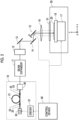
- a laser annealing apparatus will be described with reference to Figs. 1 to 7B .
- Fig. 1 is a schematic perspective view of a laser annealing apparatus according to an example.
- a laser light source 10 outputs a pulsed laser beam.
- the pulsed laser beam output from the laser light source 10 is incident on a laser irradiation surface of a semiconductor wafer 20, which is an annealing target, via a beam expander 11, a beam shaping optical element 12, folding mirrors 13 and 14, a beam scanner 15, and an f ⁇ lens 16.
- the semiconductor wafer 20 is held by a wafer chuck 18 supported by a moving mechanism 17.
- the moving mechanism 17 moves the wafer chuck 18 in two directions in the horizontal plane.
- an XY stage is used as the moving mechanism 17.
- the beam expander 11 adjusts a beam size (a diameter of a beam cross section) at an incident position of a laser beam on the beam shaping optical element 12.
- the beam shaping optical element 12 shapes the shape and intensity distribution of a beam spot on the beam irradiation surface of the semiconductor wafer 20.
- a diffraction optical element is used as the beam shaping optical element 12.
- the beam scanner 15 includes a galvanometer mirror 15A and a motor 15B.
- the motor 15B rotates the galvanometer mirror 15A within a certain range in a swing direction to perform scanning with the pulsed laser beam in one-dimensional direction.
- the f ⁇ lens 16 converges the pulsed laser beam for scanning by the beam scanner 15 onto the laser irradiation surface of the semiconductor wafer 20.
- Fig. 2 is a schematic diagram of the laser annealing apparatus according to the present example. The description of the content that overlaps with that in the description of Fig. 1 is omitted.
- a fiber laser oscillator is used as the laser light source 10.
- An input-side optical fiber 32 is connected to one end of a gain fiber 31 doped with a laser active medium, and an output-side optical fiber 34 is connected to the other end of the gain fiber 31.
- a high reflectance type fiber Bragg grating 33 is formed on the input-side optical fiber 32, and a low reflectance type fiber Bragg grating 35 is formed on the output-side optical fiber 34.
- An optical resonator is configured by the high reflectance type fiber Bragg grating 33 and the low reflectance type fiber Bragg grating 35.
- Excitation light output from a laser diode 30 is introduced into the gain fiber 31 through the input-side optical fiber 32.
- the laser active medium doped in the gain fiber 31 is excited by the excitation light. Stimulated emission occurs when the laser active medium transitions to a lower energy state, and laser light is generated.
- the laser light generated by the gain fiber 31 is incident into a wavelength conversion element 36 through the output-side optical fiber 34.
- the laser beam wavelength-converted by the wavelength conversion element 36 is incident on the semiconductor wafer 20 via the beam expander 11, the beam shaping optical element 12, the folding mirrors 13 and 14, the beam scanner 15, and the f ⁇ lens 16.
- the gain fiber 31 outputs, for example, infrared region laser light, and the wavelength conversion element 36 converts the infrared region laser light into green wavelength region laser light.
- a driver 37 drives the laser diode 30, based on an instruction from a control device 40.
- the instruction that is received from the control device 40 includes information designating the repetition frequency of a laser pulse that is output from the laser diode 30.
- the driver 37 causes the laser diode 30 to output excitation laser light at the repetition frequency of the laser pulse instructed by the control device 40. As a result, a pulsed laser beam is output from the laser light source 10 at the instructed repetition frequency.
- the moving mechanism 17 and the wafer chuck 18 are disposed in a chamber 50.
- a laser transmission window 51 is mounted on the wall surface of the chamber 50 above the semiconductor wafer 20 held by the wafer chuck 18.
- the pulsed laser beam that has passed through the f ⁇ lens 16 passes through the laser transmission window 51 and is incident on the laser irradiation surface of the semiconductor wafer 20.
- the laser annealing apparatus according to the present example performs, for example, activation annealing of a dopant doped in the semiconductor wafer 20.
- the semiconductor wafer 20 is, for example, a silicon wafer.
- the control device 40 includes a console that is operated by a user. The user operates the console to input information designating the pulse repetition frequency of the pulsed laser beam. The control device 40 provides the driver 37 with the information designating the repetition frequency of the input pulse.
- the control device 40 further controls the beam scanner 15 and the moving mechanism 17 to move the beam spot on the laser irradiation surface of the semiconductor wafer 20.
- An xyz orthogonal coordinate system is defined in which the direction in which the beam spot moves in the scanning with the pulsed laser beam by the beam scanner 15 is an x direction and the direction orthogonal to the x direction in the laser irradiation surface is a y direction.
- the movement of the beam spot in the x direction in the scanning with the pulsed laser beam by the beam scanner 15 is called "sweep".
- the control device 40 performs annealing of the semiconductor wafer 20 by sweeping the beam spot in the x direction by controlling the beam scanner 15 while moving the semiconductor wafer 20 in the y direction by controlling the moving mechanism 17.
- the maximum length in which the beam spot can sweep in the x direction depends on the swing angle of the pulsed laser beam by the beam scanner 15 and the performance of the f ⁇ lens 16. In a case where the maximum length of the sweep is shorter than the dimension of the semiconductor wafer 20, the processing of sweeping the beam spot in the x direction while moving the semiconductor wafer 20 in the y direction is repeated several times while moving the semiconductor wafer 20 in the x direction, so that almost the entire area of the semiconductor wafer 20 can be annealed.
- t is an elapsed time from the start of heating
- C is the specific heat of the semiconductor wafer
- ⁇ is the density of the semiconductor wafer
- ⁇ is the thermal conductivity of the semiconductor wafer 20.
- the unit of the surface temperature T is "K”
- the unit of the power density P is "W/cm 2 "
- the unit of the elapsed time t is "second”
- the unit of the specific heat C is "J/g ⁇ K”
- the unit of the density ⁇ is "g/cm3
- the unit of the thermal conductivity ⁇ is "W/cm ⁇ K".
- T a 2 P t 0 ⁇ C ⁇
- the power density P and the pulse width t 0 required to raise the temperature to the target value are determined.
- Fig. 3 is a graph showing calculated values in a temporal change of the surface temperature T when one shot of the pulsed laser beam is incident on a silicon wafer.
- the horizontal axis represents the elapsed time t from the point in time of rising of the laser pulse in the unit of "ns”
- the left vertical axis represents the surface temperature T of the semiconductor wafer 20 in the unit of "°C”
- the right vertical axis represents the power density P of the pulsed laser beam in the unit of "MW/cm 2 ".
- a dashed line in the graph indicates a temporal change in the power density P of the pulsed laser beam
- a solid line indicates a temporal change in the surface temperature T of the semiconductor wafer 20.
- the pulse width of the pulsed laser beam is t 0 and the peak power density is 5 MW/cm 2 .
- the surface temperature T rises according to Expression (1).
- the surface temperature T is gradually lowered.
- Fig. 4 is a sectional view of the semiconductor wafer 20 on which the pulsed laser beam is incident.
- the incident position of the laser beam becomes a heat source Pf.
- a temperature rise amount ⁇ T at the position Pr on the non-irradiation surface immediately below the heat source Pf is expressed by the following expression.
- ⁇ T Q 2 ⁇ h e ⁇ vh 2 k
- Q is input heat from the heat source Pf to the semiconductor wafer 20
- h is the thickness of the semiconductor wafer 20
- v is a sweep speed of the heat source Pr
- k is the thermal diffusivity of the semiconductor wafer 20.
- the unit of the input heat Q is "W”
- the unit of the thickness h of the semiconductor wafer 20 is "cm”
- the unit of the sweep speed v is "cm/s”
- the unit of the thermal diffusivity k is "cm 2 /s”.
- Figs. 5A and 5B are graphs showing examples of the calculation results of the temperature distribution within the cross section of the semiconductor wafer 20.
- Figs. 5A and 5B show the temperature distributions in the cross section of the wafer at a finite thickness and under an adiabatic condition of the non-irradiation surface.
- the horizontal axis represents the position of the heat source Pf in a sweep direction.
- the current position of the heat source Pf is set to be the origin of the horizontal axis, and a moving direction of the heat source is set to be positive.
- the vertical axis represents a depth from the beam irradiation surface in the unit of " ⁇ m". Figs.
- FIG. 5A and 5B show the temperature distributions in a case where the sweep speeds v of the heat source Pf are different.
- Fig. 5B shows the temperature distribution in a case where the sweep speed v of the heat source Pf is faster than that in Fig. 5A .
- the curves in the graph represent isothermal lines, and the numerical value attached to each curve represents a temperature in the unit of "°C".
- the temperature gradient in the thickness direction is gentler than that in a case where the sweep speed v is fast ( Fig. 5B ). That is, in a case where the sweep speed v is slow, the temperature rise amount ⁇ T of the non-irradiation surface is larger than that in a case where the sweep speed v is fast. In other words, the temperature rise amount ⁇ T of the non-irradiation surface can be reduced by increasing the sweep speed v.
- Fig. 6 is a flowchart showing the procedure of the laser annealing method according to the present example.
- the laser power and the beam size on the beam irradiation surface are determined from a first target value of the highest attainment temperature of the laser irradiation surface of the semiconductor wafer 20 (step S1).
- the power density P can be determined from the laser power and the beam size.
- the first target value of the highest attainment temperature can be determined based on the melting point of the semiconductor wafer 20. For example, in a case where it is desired to melt the surface layer portion of the semiconductor wafer 20, it is favorable if the highest attainment temperature is set to be equal to or higher than the melting point. In a case where it is desired to perform annealing without melting, it is favorable if the highest attainment temperature is set to be lower than the melting point.
- the pulse repetition frequency and the sweep speed v are determined under the condition that two consecutive shots of the beam spots partially overlap each other or are in contact with each other and under the condition that the highest attainment temperature of the non-irradiation surface is equal to or lower than a second target value (step S2) . It is favorable if the second target value of the highest attainment temperature of the non-irradiation surface is set to, for example, a temperature in the extent that the protective tape attached to the non-irradiation surface is not damaged.
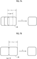
- Figs. 7A and 7B are schematic diagrams showing a movement history of a beam spot 25.
- Fig. 7A shows an example in which two consecutive shots of the beam spots 25 partially overlap each other
- Fig. 7B shows an example in which two consecutive shots of the beam spots 25 are in contact with each other.
- the dimension in the sweep direction of the beam spot is denoted by L
- the dimension in the sweep direction of the region where two consecutive shots of the beam spots overlap each other is denoted by Lov.
- Laser annealing is performed at the laser power and beam size determined in step S1 shown in Fig. 6 , and the pulse repetition frequency and the sweep speed of the beam spot determined in step S2 (step S3).
- the sweeping of the beam spot 25 is performed by performing scanning with the pulsed laser beam by the beam scanner 15. Therefore, by moving the semiconductor wafer 20 by operating the moving mechanism 17, it is possible to make the sweep speed v faster compared to a case of sweeping the beam spot on the laser irradiation surface.
- the upper limit value of the sweep speed v is limited by the product of the pulse repetition frequency f of the pulsed laser beam and the beam size L. In order to increase the upper limit value of the sweep speed v, it is desirable to increase the pulse repetition frequency f and increase the beam size L.
- the beam size L is increased under the condition that the laser power is kept constant, the power density P on the laser irradiation surface of the semiconductor wafer 20 is reduced.
- the pulse width t 0 has to be increased. If the pulse width t 0 is increased, the amount of heat transferred in the thickness direction during the period in which the laser pulse is incident is increased. As a result, the temperature of the irradiated surface increases. Therefore, the beam size L cannot be unconditionally increased.
- the pulse repetition frequency f is increased.
- the pulse repetition frequency f is preferably 15 kHz or more, and more preferably 100 kHz or more.
- the pulse repetition frequency f In a case where the pulse repetition frequency f is low, the influence of the temperature rise of the laser irradiation surface due to the immediately preceding shot is eliminated, and after the temperature has decreased to the original temperature, the next shot is incident on the semiconductor wafer 20. If the pulse repetition frequency f is increased, the next shot is performed in a state where the thermal effect due to the immediately preceding shot remains. In particular, if the pulse repetition frequency f is set to 15 kHz or more, the next shot is incident in a state where a temperature rise of 1% or more of the temperature rise amount ⁇ T of the laser irradiation surface due to the immediately preceding shot remains.
- the pulse repetition frequency f is set to 100 kHz or more, the next shot is incident in a state where a temperature rise of 5% or more of the temperature rise amount ⁇ T of the laser irradiation surface due to the immediately preceding shot remains. Therefore, the beam irradiation surface can be heated more efficiently.
- the fiber laser is used as the laser light source 10 ( Figs. 1 and 2 ).
- a mode-locked laser or the like may be used.
- the pulsed laser is used for laser annealing.
- a continuous wave (CW) laser may be used.
- the CW laser corresponds to a case where the pulse repetition frequency f of the pulsed laser is set to an infinity.
- the galvanometer scanner is used for sweeping of the beam spot at the sweep speed v.
- the beam spot may sweep on the laser irradiation surface of the semiconductor wafer 20 by fixing the path of the laser beam and moving the semiconductor wafer 20.
Landscapes
- Physics & Mathematics (AREA)
- Optics & Photonics (AREA)
- Engineering & Computer Science (AREA)
- Plasma & Fusion (AREA)
- Mechanical Engineering (AREA)
- Electromagnetism (AREA)
- Recrystallisation Techniques (AREA)
- Laser Beam Processing (AREA)
- Health & Medical Sciences (AREA)
- Toxicology (AREA)
Applications Claiming Priority (2)
| Application Number | Priority Date | Filing Date | Title |
|---|---|---|---|
| JP2020104999 | 2020-06-18 | ||
| PCT/JP2021/022562 WO2021256434A1 (ja) | 2020-06-18 | 2021-06-14 | レーザアニール装置の制御装置及びレーザアニール方法 |
Publications (2)
| Publication Number | Publication Date |
|---|---|
| EP4170699A1 true EP4170699A1 (de) | 2023-04-26 |
| EP4170699A4 EP4170699A4 (de) | 2023-12-13 |
Family
ID=79268055
Family Applications (1)
| Application Number | Title | Priority Date | Filing Date |
|---|---|---|---|
| EP21826251.7A Pending EP4170699A4 (de) | 2020-06-18 | 2021-06-14 | Steuerungsvorrichtung für laserglühvorrichtung und laserglühverfahren |
Country Status (6)
| Country | Link |
|---|---|
| US (1) | US12263537B2 (de) |
| EP (1) | EP4170699A4 (de) |
| JP (1) | JP7817930B2 (de) |
| KR (1) | KR20230028284A (de) |
| CN (1) | CN115803852B (de) |
| WO (1) | WO2021256434A1 (de) |
Families Citing this family (3)
| Publication number | Priority date | Publication date | Assignee | Title |
|---|---|---|---|---|
| WO2021256434A1 (ja) * | 2020-06-18 | 2021-12-23 | 住友重機械工業株式会社 | レーザアニール装置の制御装置及びレーザアニール方法 |
| WO2024018785A1 (ja) * | 2022-07-19 | 2024-01-25 | 住友重機械工業株式会社 | ビーム調整装置、レーザアニール装置 |
| CN117174622B (zh) * | 2023-10-31 | 2024-02-06 | 季华恒一(佛山)半导体科技有限公司 | 一种用于碳化硅晶圆的激光退火系统和方法 |
Family Cites Families (22)
| Publication number | Priority date | Publication date | Assignee | Title |
|---|---|---|---|---|
| RU1758964C (ru) * | 1991-01-31 | 1994-08-30 | Научно-исследовательский институт технологии и организации производства двигателей | Способ лазерной сварки |
| EP0542656A1 (de) * | 1991-10-31 | 1993-05-19 | International Business Machines Corporation | Musterübertragung durch überdeckende Beleuchtung von gemusterten Wärmeleitern und gemusterten Wärmeisolatoren auf einen thermischen Leiter |
| JPH0741845A (ja) * | 1993-07-30 | 1995-02-10 | A G Technol Kk | ビームアニール装置とそれを用いたtft製造方法 |
| JP4498716B2 (ja) * | 2002-10-03 | 2010-07-07 | 株式会社半導体エネルギー研究所 | レーザ照射装置及び前記レーザ照射装置を用いた半導体装置の作製方法 |
| US7259082B2 (en) * | 2002-10-03 | 2007-08-21 | Semiconductor Energy Laboratory Co., Ltd. | Method of manufacturing semiconductor device |
| US20050189329A1 (en) * | 2003-09-02 | 2005-09-01 | Somit Talwar | Laser thermal processing with laser diode radiation |
| WO2009039184A2 (en) * | 2007-09-19 | 2009-03-26 | Gsi Group Corporation | Link processing with high speed beam deflection |
| JP5605821B2 (ja) * | 2008-06-11 | 2014-10-15 | ワイエイシイフェトン株式会社 | レーザアニール装置 |
| RU2400907C1 (ru) * | 2009-06-23 | 2010-09-27 | Александр Владимирович Левин | Способ изготовления ротора высокооборотной электрической машины |
| JP5246716B2 (ja) | 2009-11-25 | 2013-07-24 | 株式会社日本製鋼所 | 半導体基板の製造方法及びレーザアニール装置 |
| JP4678700B1 (ja) | 2009-11-30 | 2011-04-27 | 株式会社日本製鋼所 | レーザアニール装置およびレーザアニール方法 |
| JP5590925B2 (ja) * | 2010-03-10 | 2014-09-17 | 住友重機械工業株式会社 | 半導体装置の製造方法及びレーザアニール装置 |
| JP2012011402A (ja) * | 2010-06-30 | 2012-01-19 | Sharp Corp | ワークの加工方法、ワークの加工用光照射装置およびそれに用いるプログラム |
| JP5786557B2 (ja) * | 2011-08-25 | 2015-09-30 | 株式会社Sumco | シミュレーションによるレーザースパイクアニールを施す際に生じる酸素析出物からの発生転位予測方法 |
| JP5679940B2 (ja) * | 2011-09-29 | 2015-03-04 | 住友重機械工業株式会社 | レーザアニール装置、及びレーザアニール方法 |
| SG10201503478UA (en) * | 2012-06-11 | 2015-06-29 | Ultratech Inc | Laser annealing systems and methods with ultra-short dwell times |
| JP6245678B2 (ja) * | 2012-08-08 | 2017-12-13 | 住友重機械工業株式会社 | 半導体装置の製造方法 |
| JP5865303B2 (ja) * | 2013-07-12 | 2016-02-17 | アイシン精機株式会社 | レーザ処理装置、およびレーザ処理方法 |
| US10083843B2 (en) * | 2014-12-17 | 2018-09-25 | Ultratech, Inc. | Laser annealing systems and methods with ultra-short dwell times |
| JP2019071373A (ja) * | 2017-10-11 | 2019-05-09 | 三菱電機株式会社 | 熱処理方法および熱処理装置 |
| JP7140338B2 (ja) * | 2017-12-21 | 2022-09-21 | ギガフォトン株式会社 | レーザ照射方法、及びレーザ照射システム |
| WO2021256434A1 (ja) * | 2020-06-18 | 2021-12-23 | 住友重機械工業株式会社 | レーザアニール装置の制御装置及びレーザアニール方法 |
-
2021
- 2021-06-14 WO PCT/JP2021/022562 patent/WO2021256434A1/ja not_active Ceased
- 2021-06-14 KR KR1020227044197A patent/KR20230028284A/ko active Pending
- 2021-06-14 CN CN202180043232.3A patent/CN115803852B/zh active Active
- 2021-06-14 EP EP21826251.7A patent/EP4170699A4/de active Pending
- 2021-06-14 JP JP2022531813A patent/JP7817930B2/ja active Active
-
2022
- 2022-12-16 US US18/067,121 patent/US12263537B2/en active Active
Also Published As
| Publication number | Publication date |
|---|---|
| WO2021256434A1 (ja) | 2021-12-23 |
| US20230120514A1 (en) | 2023-04-20 |
| EP4170699A4 (de) | 2023-12-13 |
| JP7817930B2 (ja) | 2026-02-19 |
| CN115803852A (zh) | 2023-03-14 |
| US12263537B2 (en) | 2025-04-01 |
| JPWO2021256434A1 (de) | 2021-12-23 |
| KR20230028284A (ko) | 2023-02-28 |
| CN115803852B (zh) | 2026-02-03 |
Similar Documents
| Publication | Publication Date | Title |
|---|---|---|
| US12263537B2 (en) | Control device for laser annealing apparatus and laser annealing method | |
| CN105719958B (zh) | 具有超短停留时间的激光退火系统及方法 | |
| US7879741B2 (en) | Laser thermal annealing of lightly doped silicon substrates | |
| JP4678700B1 (ja) | レーザアニール装置およびレーザアニール方法 | |
| JP5826027B2 (ja) | レーザベースの材料加工方法及びシステム | |
| CN1926728A (zh) | 工业用直接二极管泵浦超快速放大器系统 | |
| JP2002192368A (ja) | レーザ加工装置 | |
| KR102904611B1 (ko) | 레이저어닐링방법 및 레이저제어장치 | |
| CN103038862A (zh) | 激光退火方法及其装置 | |
| JP5661009B2 (ja) | 半導体装置の製造方法 | |
| EP4123685B1 (de) | Steuervorrichtung einer glühvorrichtung, glühvorrichtung und glühverfahren | |
| JP2012156390A (ja) | レーザアニール方法及びレーザアニール装置 | |
| JP2015115401A (ja) | レーザアニール方法およびレーザアニール装置 | |
| CN109455917B (zh) | 玻璃基板的残余应力降低方法及残余应力降低装置 | |
| JP6889922B2 (ja) | ガラス基板の残留応力低減方法及びガラス基板の残留応力低減装置 |
Legal Events
| Date | Code | Title | Description |
|---|---|---|---|
| STAA | Information on the status of an ep patent application or granted ep patent |
Free format text: STATUS: THE INTERNATIONAL PUBLICATION HAS BEEN MADE |
|
| PUAI | Public reference made under article 153(3) epc to a published international application that has entered the european phase |
Free format text: ORIGINAL CODE: 0009012 |
|
| STAA | Information on the status of an ep patent application or granted ep patent |
Free format text: STATUS: REQUEST FOR EXAMINATION WAS MADE |
|
| 17P | Request for examination filed |
Effective date: 20221221 |
|
| AK | Designated contracting states |
Kind code of ref document: A1 Designated state(s): AL AT BE BG CH CY CZ DE DK EE ES FI FR GB GR HR HU IE IS IT LI LT LU LV MC MK MT NL NO PL PT RO RS SE SI SK SM TR |
|
| DAV | Request for validation of the european patent (deleted) | ||
| DAX | Request for extension of the european patent (deleted) | ||
| STAA | Information on the status of an ep patent application or granted ep patent |
Free format text: STATUS: EXAMINATION IS IN PROGRESS |
|
| A4 | Supplementary search report drawn up and despatched |
Effective date: 20231115 |
|
| RIC1 | Information provided on ipc code assigned before grant |
Ipc: H01L 21/67 20060101ALI20231109BHEP Ipc: H01L 21/324 20060101ALI20231109BHEP Ipc: B23K 103/00 20060101ALI20231109BHEP Ipc: B23K 101/40 20060101ALI20231109BHEP Ipc: B23K 26/354 20140101ALI20231109BHEP Ipc: B23K 26/352 20140101ALI20231109BHEP Ipc: B23K 26/08 20140101ALI20231109BHEP Ipc: B23K 26/082 20140101ALI20231109BHEP Ipc: B23K 26/0622 20140101ALI20231109BHEP Ipc: H01L 21/268 20060101ALI20231109BHEP Ipc: H01L 21/265 20060101AFI20231109BHEP |
|
| 17Q | First examination report despatched |
Effective date: 20231127 |