EP4170635A1 - Anzeigetafel und anzeigevorrichtung - Google Patents
Anzeigetafel und anzeigevorrichtung Download PDFInfo
- Publication number
- EP4170635A1 EP4170635A1 EP20929681.3A EP20929681A EP4170635A1 EP 4170635 A1 EP4170635 A1 EP 4170635A1 EP 20929681 A EP20929681 A EP 20929681A EP 4170635 A1 EP4170635 A1 EP 4170635A1
- Authority
- EP
- European Patent Office
- Prior art keywords
- layer
- display panel
- substrate
- driving device
- driving circuit
- Prior art date
- Legal status (The legal status is an assumption and is not a legal conclusion. Google has not performed a legal analysis and makes no representation as to the accuracy of the status listed.)
- Pending
Links
- 239000000758 substrate Substances 0.000 claims abstract description 113
- 239000000463 material Substances 0.000 claims description 12
- 238000009413 insulation Methods 0.000 claims description 9
- 238000005538 encapsulation Methods 0.000 claims description 7
- 239000010410 layer Substances 0.000 description 207
- 239000010409 thin film Substances 0.000 description 12
- 238000005452 bending Methods 0.000 description 6
- 238000000034 method Methods 0.000 description 5
- 238000010586 diagram Methods 0.000 description 3
- 239000002184 metal Substances 0.000 description 3
- 230000005540 biological transmission Effects 0.000 description 2
- 230000000694 effects Effects 0.000 description 2
- 239000012044 organic layer Substances 0.000 description 2
- OFIYHXOOOISSDN-UHFFFAOYSA-N tellanylidenegallium Chemical compound [Te]=[Ga] OFIYHXOOOISSDN-UHFFFAOYSA-N 0.000 description 2
- 239000004642 Polyimide Substances 0.000 description 1
- 230000004888 barrier function Effects 0.000 description 1
- 230000009286 beneficial effect Effects 0.000 description 1
- 238000011161 development Methods 0.000 description 1
- 230000018109 developmental process Effects 0.000 description 1
- 238000005516 engineering process Methods 0.000 description 1
- 239000011521 glass Substances 0.000 description 1
- 238000004519 manufacturing process Methods 0.000 description 1
- 229920001721 polyimide Polymers 0.000 description 1
- 239000010453 quartz Substances 0.000 description 1
- VYPSYNLAJGMNEJ-UHFFFAOYSA-N silicon dioxide Inorganic materials O=[Si]=O VYPSYNLAJGMNEJ-UHFFFAOYSA-N 0.000 description 1
Images


Classifications
-
- H—ELECTRICITY
- H10—SEMICONDUCTOR DEVICES; ELECTRIC SOLID-STATE DEVICES NOT OTHERWISE PROVIDED FOR
- H10K—ORGANIC ELECTRIC SOLID-STATE DEVICES
- H10K59/00—Integrated devices, or assemblies of multiple devices, comprising at least one organic light-emitting element covered by group H10K50/00
- H10K59/10—OLED displays
- H10K59/12—Active-matrix OLED [AMOLED] displays
- H10K59/121—Active-matrix OLED [AMOLED] displays characterised by the geometry or disposition of pixel elements
- H10K59/1213—Active-matrix OLED [AMOLED] displays characterised by the geometry or disposition of pixel elements the pixel elements being TFTs
-
- G—PHYSICS
- G09—EDUCATION; CRYPTOGRAPHY; DISPLAY; ADVERTISING; SEALS
- G09F—DISPLAYING; ADVERTISING; SIGNS; LABELS OR NAME-PLATES; SEALS
- G09F9/00—Indicating arrangements for variable information in which the information is built-up on a support by selection or combination of individual elements
- G09F9/30—Indicating arrangements for variable information in which the information is built-up on a support by selection or combination of individual elements in which the desired character or characters are formed by combining individual elements
-
- G—PHYSICS
- G02—OPTICS
- G02F—OPTICAL DEVICES OR ARRANGEMENTS FOR THE CONTROL OF LIGHT BY MODIFICATION OF THE OPTICAL PROPERTIES OF THE MEDIA OF THE ELEMENTS INVOLVED THEREIN; NON-LINEAR OPTICS; FREQUENCY-CHANGING OF LIGHT; OPTICAL LOGIC ELEMENTS; OPTICAL ANALOGUE/DIGITAL CONVERTERS
- G02F1/00—Devices or arrangements for the control of the intensity, colour, phase, polarisation or direction of light arriving from an independent light source, e.g. switching, gating or modulating; Non-linear optics
- G02F1/01—Devices or arrangements for the control of the intensity, colour, phase, polarisation or direction of light arriving from an independent light source, e.g. switching, gating or modulating; Non-linear optics for the control of the intensity, phase, polarisation or colour
- G02F1/13—Devices or arrangements for the control of the intensity, colour, phase, polarisation or direction of light arriving from an independent light source, e.g. switching, gating or modulating; Non-linear optics for the control of the intensity, phase, polarisation or colour based on liquid crystals, e.g. single liquid crystal display cells
- G02F1/133—Constructional arrangements; Operation of liquid crystal cells; Circuit arrangements
- G02F1/1333—Constructional arrangements; Manufacturing methods
- G02F1/1345—Conductors connecting electrodes to cell terminals
- G02F1/13454—Drivers integrated on the active matrix substrate
-
- H—ELECTRICITY
- H10—SEMICONDUCTOR DEVICES; ELECTRIC SOLID-STATE DEVICES NOT OTHERWISE PROVIDED FOR
- H10D—INORGANIC ELECTRIC SEMICONDUCTOR DEVICES
- H10D86/00—Integrated devices formed in or on insulating or conducting substrates, e.g. formed in silicon-on-insulator [SOI] substrates or on stainless steel or glass substrates
- H10D86/40—Integrated devices formed in or on insulating or conducting substrates, e.g. formed in silicon-on-insulator [SOI] substrates or on stainless steel or glass substrates characterised by multiple TFTs
- H10D86/441—Interconnections, e.g. scanning lines
-
- H—ELECTRICITY
- H10—SEMICONDUCTOR DEVICES; ELECTRIC SOLID-STATE DEVICES NOT OTHERWISE PROVIDED FOR
- H10K—ORGANIC ELECTRIC SOLID-STATE DEVICES
- H10K50/00—Organic light-emitting devices
- H10K50/80—Constructional details
- H10K50/84—Passivation; Containers; Encapsulations
- H10K50/844—Encapsulations
-
- H—ELECTRICITY
- H10—SEMICONDUCTOR DEVICES; ELECTRIC SOLID-STATE DEVICES NOT OTHERWISE PROVIDED FOR
- H10K—ORGANIC ELECTRIC SOLID-STATE DEVICES
- H10K50/00—Organic light-emitting devices
- H10K50/80—Constructional details
- H10K50/86—Arrangements for improving contrast, e.g. preventing reflection of ambient light
-
- H—ELECTRICITY
- H10—SEMICONDUCTOR DEVICES; ELECTRIC SOLID-STATE DEVICES NOT OTHERWISE PROVIDED FOR
- H10K—ORGANIC ELECTRIC SOLID-STATE DEVICES
- H10K59/00—Integrated devices, or assemblies of multiple devices, comprising at least one organic light-emitting element covered by group H10K50/00
- H10K59/10—OLED displays
- H10K59/12—Active-matrix OLED [AMOLED] displays
- H10K59/122—Pixel-defining structures or layers, e.g. banks
-
- H—ELECTRICITY
- H10—SEMICONDUCTOR DEVICES; ELECTRIC SOLID-STATE DEVICES NOT OTHERWISE PROVIDED FOR
- H10K—ORGANIC ELECTRIC SOLID-STATE DEVICES
- H10K59/00—Integrated devices, or assemblies of multiple devices, comprising at least one organic light-emitting element covered by group H10K50/00
- H10K59/10—OLED displays
- H10K59/12—Active-matrix OLED [AMOLED] displays
- H10K59/127—Active-matrix OLED [AMOLED] displays comprising two substrates, e.g. display comprising OLED array and TFT driving circuitry on different substrates
- H10K59/1275—Electrical connections of the two substrates
-
- H—ELECTRICITY
- H10—SEMICONDUCTOR DEVICES; ELECTRIC SOLID-STATE DEVICES NOT OTHERWISE PROVIDED FOR
- H10K—ORGANIC ELECTRIC SOLID-STATE DEVICES
- H10K59/00—Integrated devices, or assemblies of multiple devices, comprising at least one organic light-emitting element covered by group H10K50/00
- H10K59/10—OLED displays
- H10K59/12—Active-matrix OLED [AMOLED] displays
- H10K59/129—Chiplets
-
- H—ELECTRICITY
- H10—SEMICONDUCTOR DEVICES; ELECTRIC SOLID-STATE DEVICES NOT OTHERWISE PROVIDED FOR
- H10K—ORGANIC ELECTRIC SOLID-STATE DEVICES
- H10K59/00—Integrated devices, or assemblies of multiple devices, comprising at least one organic light-emitting element covered by group H10K50/00
- H10K59/10—OLED displays
- H10K59/12—Active-matrix OLED [AMOLED] displays
- H10K59/131—Interconnections, e.g. wiring lines or terminals
-
- H—ELECTRICITY
- H10—SEMICONDUCTOR DEVICES; ELECTRIC SOLID-STATE DEVICES NOT OTHERWISE PROVIDED FOR
- H10K—ORGANIC ELECTRIC SOLID-STATE DEVICES
- H10K77/00—Constructional details of devices covered by this subclass and not covered by groups H10K10/80, H10K30/80, H10K50/80 or H10K59/80
- H10K77/10—Substrates, e.g. flexible substrates
- H10K77/111—Flexible substrates
-
- H—ELECTRICITY
- H10—SEMICONDUCTOR DEVICES; ELECTRIC SOLID-STATE DEVICES NOT OTHERWISE PROVIDED FOR
- H10K—ORGANIC ELECTRIC SOLID-STATE DEVICES
- H10K2102/00—Constructional details relating to the organic devices covered by this subclass
- H10K2102/301—Details of OLEDs
- H10K2102/311—Flexible OLED
-
- H—ELECTRICITY
- H10—SEMICONDUCTOR DEVICES; ELECTRIC SOLID-STATE DEVICES NOT OTHERWISE PROVIDED FOR
- H10K—ORGANIC ELECTRIC SOLID-STATE DEVICES
- H10K2102/00—Constructional details relating to the organic devices covered by this subclass
- H10K2102/301—Details of OLEDs
- H10K2102/351—Thickness
-
- H—ELECTRICITY
- H10—SEMICONDUCTOR DEVICES; ELECTRIC SOLID-STATE DEVICES NOT OTHERWISE PROVIDED FOR
- H10K—ORGANIC ELECTRIC SOLID-STATE DEVICES
- H10K59/00—Integrated devices, or assemblies of multiple devices, comprising at least one organic light-emitting element covered by group H10K50/00
- H10K59/10—OLED displays
- H10K59/12—Active-matrix OLED [AMOLED] displays
- H10K59/124—Insulating layers formed between TFT elements and OLED elements
-
- H—ELECTRICITY
- H10—SEMICONDUCTOR DEVICES; ELECTRIC SOLID-STATE DEVICES NOT OTHERWISE PROVIDED FOR
- H10K—ORGANIC ELECTRIC SOLID-STATE DEVICES
- H10K59/00—Integrated devices, or assemblies of multiple devices, comprising at least one organic light-emitting element covered by group H10K50/00
- H10K59/10—OLED displays
- H10K59/12—Active-matrix OLED [AMOLED] displays
- H10K59/127—Active-matrix OLED [AMOLED] displays comprising two substrates, e.g. display comprising OLED array and TFT driving circuitry on different substrates
-
- H—ELECTRICITY
- H10—SEMICONDUCTOR DEVICES; ELECTRIC SOLID-STATE DEVICES NOT OTHERWISE PROVIDED FOR
- H10K—ORGANIC ELECTRIC SOLID-STATE DEVICES
- H10K59/00—Integrated devices, or assemblies of multiple devices, comprising at least one organic light-emitting element covered by group H10K50/00
- H10K59/80—Constructional details
- H10K59/87—Passivation; Containers; Encapsulations
- H10K59/873—Encapsulations
-
- Y—GENERAL TAGGING OF NEW TECHNOLOGICAL DEVELOPMENTS; GENERAL TAGGING OF CROSS-SECTIONAL TECHNOLOGIES SPANNING OVER SEVERAL SECTIONS OF THE IPC; TECHNICAL SUBJECTS COVERED BY FORMER USPC CROSS-REFERENCE ART COLLECTIONS [XRACs] AND DIGESTS
- Y02—TECHNOLOGIES OR APPLICATIONS FOR MITIGATION OR ADAPTATION AGAINST CLIMATE CHANGE
- Y02E—REDUCTION OF GREENHOUSE GAS [GHG] EMISSIONS, RELATED TO ENERGY GENERATION, TRANSMISSION OR DISTRIBUTION
- Y02E10/00—Energy generation through renewable energy sources
- Y02E10/50—Photovoltaic [PV] energy
- Y02E10/549—Organic PV cells
Definitions
- the present disclosure relates to a field of display, and more particularly, to a display panel and a display device.
- Lower bezels of display panels of conventional mobile phones generally use a chip on FPC (COF) or a chip on Pi (COP) process to arrange a position of a driving chip, such that spacing of the lower bezels of the display panels are small.
- COF chip on FPC
- COP chip on Pi
- a bending portion and GOA circuits located on both lateral sides of the display panel still occupy certain spacing, so that reduction of the bezel can not be further realized.
- the present disclosure provides a display panel and a display device to solve the technical problem that the bezel spacing of the conventional display panel is too large.
- the present disclosure provides a display panel, including: a first substrate, a first driving circuit layer located on the first substrate, a second substrate located on the first driving circuit layer, a second driving circuit layer located on the second substrate, and a pixel electrode layer located on the second driving circuit layer; wherein orthographic projections of a gate driving device and a source driving device in the first driving circuit layer projected on the first substrate are located within a display area of the display panel.
- the first driving circuit layer includes the gate driving device located on at least one side of the display panel, the gate driving device includes at least one gate driving unit, and one said gate driving unit is electrically connected to at least one scanning line of the second driving circuit layer by a plurality of first via holes;
- the second driving circuit layer includes an active layer located on the second substrate, a gate insulating layer located on the active layer, a gate layer located on the gate insulating layer, an inter-insulation layer located on the gate layer, a source-drain layer located on the inter-insulation layer, and a planarization layer located on the source-drain layer; wherein the first via holes pass through the gate insulating layer and the second substrate, and the second via holes pass through the inter-insulating layer, the gate insulating layer and the second substrate.
- the first via holes and the second via holes are positioned near an edge of the display panel.
- the display panel further includes first fan-out traces connecting the gate driving device and a binding layer of the display panel, and second fan-out traces connecting the source driving device and the binding layer of the display panel;
- the third via holes and the fourth via holes pass through the first driving circuit layer and the first substrate.
- the first driving circuit layer includes a first gate driving device located on a first side of the display panel and a second gate driving device located on a third side of the display panel, and a first source driving device located on a second side of the display panel; an orthographic projection of a binding layer of the display panel on the first driving circuit layer is located within an area which surrounded by the first gate driving device, the second gate driving device, and the first source driving device.
- the gate driving device and the source driving device are located in a non-pixel area between adjacent pixel units of the display panel.
- the first substrate and the second substrate are made of flexible materials, and each of the first substrate and the second substrate has a thickness being from 1 micrometer to 10 micrometers.
- the display panel further includes a light emitting device layer located on the second driving circuit layer, and an encapsulation layer located on the light emitting device layer.
- the present disclosure further provides a display device, the display device includes a display panel, and a polarizer layer and a cover layer located on the display panel, the display panel includes a first substrate, a first driving circuit layer located on the first substrate, a second substrate located on the first driving circuit layer, a second driving circuit layer located on the second substrate, and a pixel electrode layer located on the second driving circuit layer; wherein orthographic projections of a gate driving device and a source driving device in the first driving circuit layer projected on the first substrate are located within a display area of the display panel.
- the first driving circuit layer includes the gate driving device located on at least one side of the display panel, the gate driving device includes at least one gate driving unit, and one said gate driving unit is electrically connected to at least one scanning line of the second driving circuit layer by a plurality of first via holes;
- the second driving circuit layer includes an active layer located on the second substrate, a gate insulating layer located on the active layer, a gate layer located on the gate insulating layer, an inter-insulation layer located on the gate layer, a source-drain layer located on the inter-insulation layer, and a planarization layer located on the source-drain layer; wherein the first via holes pass through the gate insulating layer and the second substrate, and the second via holes pass through the inter-insulating layer, the gate insulating layer and the second substrate.
- the first via holes and the second via holes are positioned near an edge of the display panel.
- the display panel further includes first fan-out traces connecting the gate driving device and a binding layer of the display panel, and second fan-out traces connecting the source driving device and the binding layer of the display panel;
- the third via holes and the fourth via holes pass through the first driving circuit layer and the first substrate.
- the first driving circuit layer includes a first gate driving device located on a first side of the display panel and a second gate driving device located on a third side of the display panel, and a first source driving device located on a second side of the display panel; an orthographic projection of a binding layer of the display panel on the first driving circuit layer is located within an area which surrounded by the first gate driving device, the second gate driving device, and the first source driving device.
- the gate driving device and the source driving device are located in a non-pixel area between adjacent pixel units of the display panel.
- the first substrate and the second substrate are made of flexible materials, and each of the first substrate and the second substrate has a thickness being from 1 micrometer to 10 micrometers.
- the display panel further includes a light emitting device layer located on the second driving circuit layer, and an encapsulation layer located on the light emitting device layer.
- the present disclosure removes a source driving device and an gate driving device originally occupying the bezel spacing, and realizes the narrow bezel design of the display panel by disposing the gate driving device and the source driving device of the display panel below the array driving layer of the display panel, and making the orthographic projections of the gate driving device and the source driving device projected on the first substrate be within the display area of the display panel.
- Lower bezels of display panels of conventional mobile phones generally use a COF or COP process to arrange a position of a driving chip, so that spacing of the lower bezels of the display panels are small.
- a bending area and GOA circuits on both lateral sides of the display panel still occupy certain spacing, so that reduction of the bezel can not be further realized.
- the present disclosure provides the following technical solutions to solve the above technical problems.
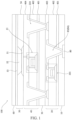
- the present disclosure provides a display panel 100 including a first substrate 1010, a first driving circuit layer 20 located on the first substrate 10, a second substrate 30 located on the first driving circuit layer 20, a second driving circuit layer 40 located on the second substrate 30, and a pixel electrode layer located on the second driving circuit layer 40;
- the orthographic projections of the gate driving device 21 and the source driving device 22 in the first driving circuit layer 20 projected on the first substrate 10 are within a display area of the display panel 100.
- the present disclosure removes a source driving device 22 and a gate driving device 21 originally occupying the bezel spacing, and realizes the narrow bezel design of the display panel 100 by disposing the gate driving device 21 and the source driving device 22 of the display panel 100 below the array driving layer of the display panel 100, and making the orthographic projections of the gate driving device 21 and the source driving device 22 projected on the first substrate 10 be within the display area of the display panel 100.
- the technical solution of the present disclosure can be applied to an OLED display panel 100 or an LCD display panel 100.
- Different types of display panels 100 correspond to different structures.
- the OLED display panel 100 is taken as an example to describe the technical solution of the present disclosure in connection with specific embodiments.
- the display panel 100 includes a first substrate 10, a first driving circuit layer 20 located on the first substrate 10, a second substrate 30 located on the first driving circuit layer 20, a second driving circuit layer 40 located on the second substrate 30, a light emitting device layer 50 located on the second driving circuit layer 40, and an encapsulation layer 60 located on the light emitting device layer 50.
- the first substrate 10 and the second substrate 30 may be rigid substrates or flexible substrates.
- the materials of the first substrate 10 and the second substrate 30 may be made of materials such as glass and quartz.
- the first substrate 10 and the second substrate 30 may be materials such as polyimide.
- the substrate structure may be a flexible substrate, which is not described in detail herein.
- the second driving circuit layer 40 includes a plurality of second thin film transistors 41.
- the second thin film transistor 41 may be a structure of an etch barrier type, a back channel etch type, or a top gate thin film transistor type etc., which is not specifically limited.
- the second thin film transistor 41 of the top gate thin film transistor type may include a buffer layer 401 located on the second substrate 30, an active layer located on the buffer layer 401, a gate insulating layer 402 located on the active layer, a gate layer located on the gate insulating layer 402, an inter-insulating layer 403 located on the gate layer, a source-drain layer located on the inter-insulation layer 403, and a planarization layer 404 located on the source-drain layer.
- the above-mentioned top-gate thin film transistor is not limited to a single-gate structure and can also be configured as a double-gate structure, etc., which is described in detail herein.
- the light emitting device layer 50 includes an anode layer 51, a light emitting layer 52, and a cathode layer 53 which are formed on the second driving circuit layer 40.
- the anode layer 51 is the pixel electrode layer described above herein.
- the anode layer 51 is formed on the planarization layer 404.
- the anode layer 51 is mainly used to provide empty holes for absorbing electrons.
- a top-emitting OLED device is taken as an example for description, and anode layer 51 may be a non-transparent or transparent metal electrode.
- the light emitting layer 52 is formed on the anode layer 51.
- the light-emitting layer 52 is divided into a plurality of light-emitting units by the pixel definition layer 54.
- the cathode layer 53 is formed on the light emitting layer 52.
- the cathode layer 53 covers the light-emitting layer 52 and the pixel define layer 54 located on the planarization layer 404.
- the materials of the anode layer 51 and the cathode layer 53 can be defined according to the light-emitting type of the display panel 100.
- the anode layer 51 may be made of a totally reflective material
- the cathode layer 53 may be made of a semi-reflective material.
- the materials of the cathode layer 53 are interchanged with the materials of the anode layer 51.
- the light emitting device layer 50 forms a microcavity effect by total reflection and semi-reflection of the anode layer 51 and the cathode layer 53 to increase the light emitting efficiency of the light emitting device layer 50.
- the display panel 100 Since a large number of light-shielding metal layers are disposed in the first driving circuit layer 20, if the display panel 100 is a bottom-emission type, a device to which the first driving circuit layer 20 corresponds can only be disposed in a non-light-transmissive area of the display panel 100, and the display panel 100 being a top-emitting type is not limited by the above. Therefore, the display panel 100 being a top emission type has a larger aperture ratio compared with the display panel 100 being a bottom emission type.
- the encapsulation layer 60 may be a thin-film encapsulation layer 60, which may include a first inorganic layer, a first organic layer located on the first inorganic layer, and a second inorganic layer located on the first organic layer.
- the specific structure is the same as or similar to the prior art and is not repeatedly described herein.
- the first driving circuit layer 20 is located between the first substrate 10 and the second substrate 30.
- the first driving circuit layer 20 is identical to the second driving circuit layer 40.
- the first driving circuit layer 20 is also provided with a plurality of first thin film transistors 201.
- first thin film transistors 201 refer to the second thin film transistor 41 in the second driving circuit layer 40.
- the structures of the first thin film transistors 201 is not repeatedly described herein.
- a combination of the plurality of first thin film transistors 201 in the first driving circuit layer 20 may constitute a corresponding gate driving device 21 or source driving device 22.
- the first driving circuit layer 20 includes the gate driving device 21 located on at least one side of the display panel 100.
- the gate driving device 21 includes at least one gate driving unit 213.
- One said gate driving unit 213 is electrically connected to at least one scan line 405 of the second driving circuit layer 40 by first via holes 214.
- the first driving circuit layer 20 may include a first gate driving device 211 located on a first side 701 of the display panel 100, and a second gate driving device 212 located on a third side 703 of the display panel 100.
- the GOA unit can scan one or more scan lines 405 simultaneously.
- the type of the gate driving unit 213 in the embodiment may be 2T1 C, 7T1C, etc. in the prior art, and is not specifically limited herein.
- the first via holes 214 pass through the second substrate 30 and a portion of the second driving circuit layer 40.
- the first via holes 214 pass through the gate insulating layer 402, the buffer layer 401, and the second substrate 30, such that the scan lines 405 in the gate layer are electrically connected with the gate driving device 21 in the first driving circuit layer 20 by the first via holes 214.
- the display panel 100 of the embodiment may input scan signals into the panel from the gate driving devices 21 on the both sides, or the first gate driving device 211 may be used to control the odd rows of scan lines 405, and the second gate driving device 212 is used to control the even rows of scan lines 405, etc.
- the specific scanning method is not introduced in detail in the present disclosure.
- the second driving circuit layer 40 includes the source driving device 22 located on at least one side of the display panel 100.
- the source driving device 22 includes at least one source driving unit 223, and one said source driving unit 223 is electrically connected with at least one data line 406 of the second driving circuit layer 40 by a second via hole 224.
- first side 701 and the third side 703 may be side bezels of the display panel 100, which are disposed oppositely.
- the display panel 100 further includes a second side 702 and a fourth side 704 disposed opposite the second side 702.
- the second side 702 and the fourth side 704 may be an upper bezel and a bottom bezel.
- the first driving circuit layer 20 may include a first source driving device 221 located on the second side 702 of the display panel 100.
- the data lines 406 of the display panel 100 extend along the direction of the first side 701 or the direction of the third side 703 toward the second side 702, and are electrically connected with the first source driving device 221 by the second via holes 224.
- the source driving units 223 in the first source driving device 221 may be electrically connected to at least one data line 406.
- the first driving circuit layer 20 may further include a second source driving device 22 located on the fourth side 704 of the display panel 100. Some of the data lines 406 are electrically connected with the first source driving device 221, and some of the data lines 406 are electrically connected with the second source driving device 22. The first source driving units 223 and the second source driving units 223 do not interfere with each other.
- the second via holes 224 pass through the second substrate 30 and a portion of the second driving circuit layer 40.
- the second via holes 224 pass through the inter-insulating layer 403, the gate insulating layer 402, the buffer layer 401, and the second substrate 30, so that the data lines 406 in the source-drain layer are electrically connected to the source driving device 22 in the first driving circuit layer 20 by the second via holes 224.
- the first via holes 214 and the second via holes 224 may be disposed near the edge of the display panel 100.
- the first via holes 214 and the second via holes 224 which are disposed at the edge of the display panel 100 may avoid the influence of the via holes on the internal structure of the panel.
- the display panel 100 may include a display layer 200 located on the first driving circuit layer 20, and a binding layer 80 located on a side of the first driving circuit layer 20 away from the display layer 200.
- the binding layer 80 is located in the first substrate 10 or located on a side of the first substrate 10 away from the light emitting device layer 50.
- the orthographic projection of the binding layer 80 on the first driving circuit layer 20 is within an area which surrounded by the first gate driving device 211, the second gate driving device 212, and the first source driving device 221 or/and the second source driving device 22.
- the display panel 100 further includes first fan-out traces 81 connecting the gate driving device 21with the binding layer 80 of the display panel 100, and the second fan-out traces 82 connecting the source driving device 22 with the binding layer 80 of the display panel 100.
- first fan-out traces 81 are electrically connected with the gate driving device 21 by third via holes 83, and the second fan-out traces 82 are electrically connected with the source driving device 22 by fourth via holes 84.
- the first fan-out traces 81 and the second fan-out traces 82 may be mounted on the same layer as the binding layer 80.
- the first fan-out traces 81 and the second fan-out traces 82 may be mounted in the first substrate 10.
- the third via holes 83 and the fourth via holes 84 pass through the first driving circuit layer 20 and the first substrate 10.
- the first fan-out traces 81 may extend along the bottom end of the gate driving device 21 near the second side 702 toward a first terminal area of the bonding layer 80, and be insulated from the second fan-out traces 82.
- the first fan-out traces 81 may extend from the bottom end of the gate driving device 21 near the fourth side 704 toward a second terminal area of the binding area.
- the technical solution of the embodiment can increase spacing between the signal lines in the first fan-out traces 81 and the second fan-out traces 82, thereby reducing the process and accuracy of the first fan-out traces 81 and the second fan-out traces 82, and preventing the signal lines from a technical problem of short circuit.
- the driver ICs or display ICs on the panel are disposed using a space in the back of the display panel 100 to reduce the lower bezel of the display panel 100.
- the bending structure of the flexible display panel 100 still has a certain bending radius, spacing of the lower bezel of the display panel 100 cannot be eliminated.
- the binding layer 80 of the embodiment is disposed on a side of the first substrate 10 away from the light emitting layer 52 of the display panel 100, such that the source driving device 22 and the gate driving device 21 of the display panel 100 can be connected with the binding layer 80 by the corresponding via holes, and the corresponding data signals are input or output directly from the bottom of the display panel 100, thereby eliminating the spacing of the lower bezel of the panel, and it can be realized that the spacing of the lower bezel of the display panel 100 is 0 .
- the gate driving device 21 and the source driving device 22 may be located in a non-pixel area between adjacent pixel units of the display panel 100.
- the light emitted by the light-emitting layer 52, or the light source of the backlight module is avoided from being blocked by the corresponding gate driving device 21 and the source driving device 22.
- each of the first substrate 10 and the second substrate 30 has a thickness being from 1 micrometer to 10 micrometers. Since the technical solution of the embodiment needs to prepare the thin film transistor on or in the flexible substrate, a certain thickness basis can ensure the planarization of the panel during a manufacturing process. In addition, the flexible substrate can also increase the bending ability or stress relief etc. of the panel.
- the data lines 406 or the scan lines 405 are electrically connected with the source and drain of each driving device in the first driving circuit layer 20 by corresponding via holes, and then transmitted to the bonding layer 80 by the signal lines in the same layer as the source and drain layers in the first driving circuit layer 20.
- the present disclosure is only illustrated with the above connection method as an example.
- the metal layers, such as the gate layer and the active layer, in the first thin film transistor 201 can be functioned as the transmission layers of the data signals, and are not limited to the above-mentioned embodiments of the present disclosure.
- the present disclosure removes a source driving device 22 and a gate driving device 21 originally occupying the bezel spacing, thereby realizing the narrow bezel design of the display panel 100, and may make the entire surface of the display panel be a display area, by disposing the gate driving device 21 and the source driving device 22 of the display panel 100 below the array driving layer of the display panel 100, and make the orthographic projections of the gate driving device 21 and the source driving device 22 projected on the first substrate 10 be within the display area of the display panel 100.
- the present disclosure also provides a display device, wherein the display device includes the above-mentioned display panel, a polarizer layer and a cover layer which are located on the display panel.
- the working principle of the display device in the embodiment is the same as or identical to the working principle of the above-mentioned display panel, and is not repeatedly described herein.
- the present disclosure provides a display panel and a display device.
- the display panel includes a first substrate, a first driving circuit layer located on the first substrate, a second substrate located on the first driving circuit layer, a second driving circuit layer on the second substrate and a pixel electrode layer located on the second driving circuit layer.
- the present disclosure removes a source driving device and a gate driving device originally occupying the bezel spacing, and realizes the narrow bezel design of the display panel by disposing the gate driving device and the source driving device of the display panel below the array driving layer of the display panel, and making the orthographic projection of the gate driving device and the source driving device projected on the first substrate be within the display area of the display panel.
Landscapes
- Engineering & Computer Science (AREA)
- Microelectronics & Electronic Packaging (AREA)
- Physics & Mathematics (AREA)
- Optics & Photonics (AREA)
- Nonlinear Science (AREA)
- General Physics & Mathematics (AREA)
- Geometry (AREA)
- Devices For Indicating Variable Information By Combining Individual Elements (AREA)
- Theoretical Computer Science (AREA)
- Mathematical Physics (AREA)
- Chemical & Material Sciences (AREA)
- Crystallography & Structural Chemistry (AREA)
- Electroluminescent Light Sources (AREA)
Applications Claiming Priority (2)
| Application Number | Priority Date | Filing Date | Title |
|---|---|---|---|
| CN202010571270.3A CN111768700B (zh) | 2020-06-22 | 2020-06-22 | 显示面板及显示装置 |
| PCT/CN2020/103058 WO2021258457A1 (zh) | 2020-06-22 | 2020-07-20 | 显示面板及显示装置 |
Publications (2)
| Publication Number | Publication Date |
|---|---|
| EP4170635A1 true EP4170635A1 (de) | 2023-04-26 |
| EP4170635A4 EP4170635A4 (de) | 2024-07-24 |
Family
ID=72721577
Family Applications (1)
| Application Number | Title | Priority Date | Filing Date |
|---|---|---|---|
| EP20929681.3A Pending EP4170635A4 (de) | 2020-06-22 | 2020-07-20 | Anzeigetafel und anzeigevorrichtung |
Country Status (6)
| Country | Link |
|---|---|
| US (1) | US11974471B2 (de) |
| EP (1) | EP4170635A4 (de) |
| JP (1) | JP7457717B2 (de) |
| KR (1) | KR102727791B1 (de) |
| CN (1) | CN111768700B (de) |
| WO (1) | WO2021258457A1 (de) |
Families Citing this family (18)
| Publication number | Priority date | Publication date | Assignee | Title |
|---|---|---|---|---|
| CN112086049A (zh) * | 2020-09-16 | 2020-12-15 | 武汉华星光电技术有限公司 | 显示面板以及电子设备 |
| JP7650654B2 (ja) * | 2020-12-22 | 2025-03-25 | 日本放送協会 | 表示装置及びその製造方法 |
| WO2022160331A1 (zh) * | 2021-02-01 | 2022-08-04 | 京东方科技集团股份有限公司 | 驱动背板及其制备方法、显示装置 |
| CN113257143A (zh) * | 2021-03-29 | 2021-08-13 | 北海惠科光电技术有限公司 | 一种显示面板、显示装置和显示面板的制造方法 |
| CN116072010A (zh) * | 2021-11-02 | 2023-05-05 | 武汉华星光电半导体显示技术有限公司 | 拼接显示面板和显示装置 |
| CN114122051B (zh) * | 2021-11-04 | 2023-07-25 | 武汉华星光电半导体显示技术有限公司 | 显示面板及其制作方法、显示装置 |
| CN114284319B (zh) * | 2021-12-14 | 2023-09-26 | 武汉华星光电半导体显示技术有限公司 | 显示面板及电子设备 |
| CN114335091A (zh) * | 2021-12-22 | 2022-04-12 | 深圳市华星光电半导体显示技术有限公司 | 柔性显示面板 |
| CN114428427B (zh) * | 2022-01-27 | 2023-10-03 | Tcl华星光电技术有限公司 | 显示面板及显示装置 |
| KR20230131316A (ko) | 2022-03-03 | 2023-09-13 | 삼성디스플레이 주식회사 | 표시 장치 및 이를 포함하는 타일형 표시 장치 |
| CN114725175A (zh) * | 2022-04-06 | 2022-07-08 | 京东方科技集团股份有限公司 | 显示面板、拼接屏及显示装置 |
| WO2023216201A1 (zh) * | 2022-05-12 | 2023-11-16 | 北京小米移动软件有限公司 | Oled显示面板、oled显示面板的像素电路及显示设备 |
| CN115207054B (zh) * | 2022-07-05 | 2024-12-27 | 武汉华星光电半导体显示技术有限公司 | 显示面板 |
| KR20240097047A (ko) | 2022-12-19 | 2024-06-27 | 삼성디스플레이 주식회사 | 표시 장치 |
| KR20240119947A (ko) | 2023-01-30 | 2024-08-07 | 삼성디스플레이 주식회사 | 화소 회로 및 화소 회로를 포함하는 표시 장치의 구동 방법 |
| CN117457697B (zh) * | 2023-02-07 | 2025-09-19 | 深圳市华星光电半导体显示技术有限公司 | 显示面板及拼接屏 |
| CN116404011B (zh) * | 2023-06-07 | 2024-05-28 | 惠科股份有限公司 | 显示面板和显示装置 |
| CN119905065B (zh) * | 2023-10-27 | 2025-09-30 | 武汉华星光电半导体显示技术有限公司 | 显示面板 |
Family Cites Families (25)
| Publication number | Priority date | Publication date | Assignee | Title |
|---|---|---|---|---|
| JPS5940072Y2 (ja) | 1982-11-27 | 1984-11-12 | 義雄 川添 | 洋凧における骨材の連結具 |
| CN102317851A (zh) | 2008-12-25 | 2012-01-11 | 株式会社普利司通 | 信息显示面板 |
| KR101456154B1 (ko) * | 2009-08-25 | 2014-11-04 | 삼성디스플레이 주식회사 | 유기 발광 조명 장치 |
| JP5304761B2 (ja) | 2010-09-28 | 2013-10-02 | カシオ計算機株式会社 | 発光装置及び電子機器 |
| JP5982094B2 (ja) * | 2011-03-22 | 2016-08-31 | セイコーエプソン株式会社 | 電気光学装置、投射型表示装置および電子機器 |
| KR20120130397A (ko) * | 2011-05-23 | 2012-12-03 | 삼성디스플레이 주식회사 | 렌즈 모듈 및 이를 갖는 표시 장치 |
| KR102006728B1 (ko) * | 2013-12-02 | 2019-08-02 | 가부시키가이샤 한도오따이 에네루기 켄큐쇼 | 표시 장치 및 그 제조방법 |
| JP2015138612A (ja) * | 2014-01-21 | 2015-07-30 | 株式会社ジャパンディスプレイ | 有機エレクトロルミネセンス表示装置 |
| JP6022118B2 (ja) | 2014-04-30 | 2016-11-09 | シャープ株式会社 | アクティブマトリクス基板及び当該アクティブマトリクス基板を備える表示装置 |
| US10582612B2 (en) * | 2014-06-30 | 2020-03-03 | Lg Display Co., Ltd. | Flexible display device with reduced bend stress wires and manufacturing method for the same |
| CN104536229B (zh) * | 2015-01-12 | 2017-02-01 | 京东方科技集团股份有限公司 | 一种阵列基板及显示面板 |
| CN104867450B (zh) | 2015-06-05 | 2017-09-19 | 京东方科技集团股份有限公司 | 阵列基板及其制作方法、显示装置 |
| JP6661904B2 (ja) * | 2015-07-01 | 2020-03-11 | Jsr株式会社 | 表示装置、および表示装置の製造方法 |
| US20170213872A1 (en) | 2016-01-27 | 2017-07-27 | Semiconductor Energy Laboratory Co., Ltd. | Display device |
| CN107256870A (zh) | 2017-06-09 | 2017-10-17 | 京东方科技集团股份有限公司 | 一种阵列基板及制作方法、柔性显示面板、显示装置 |
| CN115425052A (zh) * | 2017-06-29 | 2022-12-02 | 京东方科技集团股份有限公司 | 显示面板及显示装置 |
| KR20190010052A (ko) * | 2017-07-20 | 2019-01-30 | 엘지전자 주식회사 | 디스플레이 디바이스 |
| KR102452251B1 (ko) * | 2017-08-04 | 2022-10-11 | 삼성디스플레이 주식회사 | 표시 장치 |
| CN107978622B (zh) * | 2017-11-22 | 2020-08-11 | 上海天马有机发光显示技术有限公司 | 一种阵列基板、显示面板和显示装置 |
| WO2019215530A1 (ja) | 2018-05-11 | 2019-11-14 | 株式会社半導体エネルギー研究所 | 表示装置、及び表示装置の作製方法 |
| US11423844B2 (en) * | 2018-05-17 | 2022-08-23 | Semiconductor Energy Laboratory Co., Ltd. | Display device and electronic device |
| CN108630144A (zh) * | 2018-06-19 | 2018-10-09 | 武汉天马微电子有限公司 | 显示面板和显示装置 |
| TWI686648B (zh) * | 2019-01-08 | 2020-03-01 | 友達光電股份有限公司 | 顯示面板 |
| CN109857279B (zh) * | 2019-03-19 | 2022-04-12 | 厦门天马微电子有限公司 | 显示面板及显示装置 |
| CN110211525A (zh) | 2019-05-27 | 2019-09-06 | 福建华佳彩有限公司 | 一种面板设计架构 |
-
2020
- 2020-06-22 CN CN202010571270.3A patent/CN111768700B/zh active Active
- 2020-07-20 US US17/058,150 patent/US11974471B2/en active Active
- 2020-07-20 KR KR1020217015774A patent/KR102727791B1/ko active Active
- 2020-07-20 JP JP2021542514A patent/JP7457717B2/ja active Active
- 2020-07-20 EP EP20929681.3A patent/EP4170635A4/de active Pending
- 2020-07-20 WO PCT/CN2020/103058 patent/WO2021258457A1/zh not_active Ceased
Also Published As
| Publication number | Publication date |
|---|---|
| JP7457717B2 (ja) | 2024-03-28 |
| US11974471B2 (en) | 2024-04-30 |
| WO2021258457A1 (zh) | 2021-12-30 |
| KR102727791B1 (ko) | 2024-11-11 |
| KR20220000895A (ko) | 2022-01-04 |
| CN111768700A (zh) | 2020-10-13 |
| CN111768700B (zh) | 2021-10-08 |
| JP2022543943A (ja) | 2022-10-17 |
| US20220190074A1 (en) | 2022-06-16 |
| EP4170635A4 (de) | 2024-07-24 |
Similar Documents
| Publication | Publication Date | Title |
|---|---|---|
| US11974471B2 (en) | Display panel having a gate driving device and source driving device on different substrates | |
| US10741788B2 (en) | Display device | |
| KR102730281B1 (ko) | 관통홀이 구비된 표시장치 | |
| KR20230147024A (ko) | 표시 장치 | |
| CN107785394B (zh) | 显示装置 | |
| CN118510328A (zh) | 具有基板孔的显示设备 | |
| US12141431B2 (en) | Display device | |
| US11930688B2 (en) | Display device for blocking penetration of moisture into interior while extending cathode electrode | |
| KR102707629B1 (ko) | 표시장치 | |
| US20250275388A1 (en) | Display substrate | |
| CN118571898A (zh) | 显示装置 | |
| KR20210008739A (ko) | 디스플레이 장치 | |
| US12495682B2 (en) | Touch display device | |
| US20230413646A1 (en) | Display device | |
| JP7654044B2 (ja) | フレキシブル表示装置 | |
| US20230189573A1 (en) | Touch display device | |
| US20250266404A1 (en) | Display device | |
| US20240414984A1 (en) | Display Apparatus | |
| KR20250131516A (ko) | 표시 장치 | |
| CN120583836A (zh) | 显示装置和制造显示装置的方法 | |
| KR20250096403A (ko) | 표시 장치 | |
| KR20240103512A (ko) | 표시장치 | |
| KR20250131087A (ko) | 링크배선을 포함하는 표시장치 및 그 제조방법 | |
| KR20250055151A (ko) | 표시 장치 | |
| KR20240104893A (ko) | 표시 장치 |
Legal Events
| Date | Code | Title | Description |
|---|---|---|---|
| STAA | Information on the status of an ep patent application or granted ep patent |
Free format text: STATUS: UNKNOWN |
|
| STAA | Information on the status of an ep patent application or granted ep patent |
Free format text: STATUS: THE INTERNATIONAL PUBLICATION HAS BEEN MADE |
|
| PUAI | Public reference made under article 153(3) epc to a published international application that has entered the european phase |
Free format text: ORIGINAL CODE: 0009012 |
|
| STAA | Information on the status of an ep patent application or granted ep patent |
Free format text: STATUS: REQUEST FOR EXAMINATION WAS MADE |
|
| 17P | Request for examination filed |
Effective date: 20211014 |
|
| AK | Designated contracting states |
Kind code of ref document: A1 Designated state(s): AL AT BE BG CH CY CZ DE DK EE ES FI FR GB GR HR HU IE IS IT LI LT LU LV MC MK MT NL NO PL PT RO RS SE SI SK SM TR |
|
| DAV | Request for validation of the european patent (deleted) | ||
| DAX | Request for extension of the european patent (deleted) | ||
| A4 | Supplementary search report drawn up and despatched |
Effective date: 20240620 |
|
| RIC1 | Information provided on ipc code assigned before grant |
Ipc: H10K 59/127 20230101ALI20240614BHEP Ipc: H10K 59/12 20230101ALI20240614BHEP Ipc: H10K 59/121 20230101ALI20240614BHEP Ipc: G02F 1/1345 20060101ALI20240614BHEP Ipc: G09F 9/30 20060101AFI20240614BHEP |