EP4161052B1 - Pixeleinheit, photoelektrischer sensor, kameramodul und elektronische vorrichtung - Google Patents
Pixeleinheit, photoelektrischer sensor, kameramodul und elektronische vorrichtung Download PDFInfo
- Publication number
- EP4161052B1 EP4161052B1 EP21812616.7A EP21812616A EP4161052B1 EP 4161052 B1 EP4161052 B1 EP 4161052B1 EP 21812616 A EP21812616 A EP 21812616A EP 4161052 B1 EP4161052 B1 EP 4161052B1
- Authority
- EP
- European Patent Office
- Prior art keywords
- light
- photodiode
- lateral panel
- out surface
- photoelectric sensor
- Prior art date
- Legal status (The legal status is an assumption and is not a legal conclusion. Google has not performed a legal analysis and makes no representation as to the accuracy of the status listed.)
- Active
Links
Images


Classifications
-
- H—ELECTRICITY
- H04—ELECTRIC COMMUNICATION TECHNIQUE
- H04N—PICTORIAL COMMUNICATION, e.g. TELEVISION
- H04N23/00—Cameras or camera modules comprising electronic image sensors; Control thereof
- H04N23/10—Cameras or camera modules comprising electronic image sensors; Control thereof for generating image signals from different wavelengths
- H04N23/13—Cameras or camera modules comprising electronic image sensors; Control thereof for generating image signals from different wavelengths with multiple sensors
- H04N23/16—Optical arrangements associated therewith, e.g. for beam-splitting or for colour correction
-
- H—ELECTRICITY
- H10—SEMICONDUCTOR DEVICES; ELECTRIC SOLID-STATE DEVICES NOT OTHERWISE PROVIDED FOR
- H10F—INORGANIC SEMICONDUCTOR DEVICES SENSITIVE TO INFRARED RADIATION, LIGHT, ELECTROMAGNETIC RADIATION OF SHORTER WAVELENGTH OR CORPUSCULAR RADIATION
- H10F39/00—Integrated devices, or assemblies of multiple devices, comprising at least one element covered by group H10F30/00, e.g. radiation detectors comprising photodiode arrays
- H10F39/80—Constructional details of image sensors
- H10F39/802—Geometry or disposition of elements in pixels, e.g. address-lines or gate electrodes
-
- H—ELECTRICITY
- H04—ELECTRIC COMMUNICATION TECHNIQUE
- H04N—PICTORIAL COMMUNICATION, e.g. TELEVISION
- H04N23/00—Cameras or camera modules comprising electronic image sensors; Control thereof
- H04N23/50—Constructional details
- H04N23/54—Mounting of pick-up tubes, electronic image sensors, deviation or focusing coils
-
- G—PHYSICS
- G02—OPTICS
- G02B—OPTICAL ELEMENTS, SYSTEMS OR APPARATUS
- G02B27/00—Optical systems or apparatus not provided for by any of the groups G02B1/00 - G02B26/00, G02B30/00
- G02B27/10—Beam splitting or combining systems
-
- G—PHYSICS
- G02—OPTICS
- G02B—OPTICAL ELEMENTS, SYSTEMS OR APPARATUS
- G02B5/00—Optical elements other than lenses
- G02B5/20—Filters
- G02B5/201—Filters in the form of arrays
-
- H—ELECTRICITY
- H04—ELECTRIC COMMUNICATION TECHNIQUE
- H04N—PICTORIAL COMMUNICATION, e.g. TELEVISION
- H04N23/00—Cameras or camera modules comprising electronic image sensors; Control thereof
- H04N23/50—Constructional details
- H04N23/55—Optical parts specially adapted for electronic image sensors; Mounting thereof
-
- H—ELECTRICITY
- H04—ELECTRIC COMMUNICATION TECHNIQUE
- H04N—PICTORIAL COMMUNICATION, e.g. TELEVISION
- H04N25/00—Circuitry of solid-state image sensors [SSIS]; Control thereof
- H04N25/10—Circuitry of solid-state image sensors [SSIS]; Control thereof for transforming different wavelengths into image signals
-
- H—ELECTRICITY
- H04—ELECTRIC COMMUNICATION TECHNIQUE
- H04N—PICTORIAL COMMUNICATION, e.g. TELEVISION
- H04N5/00—Details of television systems
- H04N5/30—Transforming light or analogous information into electric information
-
- H—ELECTRICITY
- H10—SEMICONDUCTOR DEVICES; ELECTRIC SOLID-STATE DEVICES NOT OTHERWISE PROVIDED FOR
- H10F—INORGANIC SEMICONDUCTOR DEVICES SENSITIVE TO INFRARED RADIATION, LIGHT, ELECTROMAGNETIC RADIATION OF SHORTER WAVELENGTH OR CORPUSCULAR RADIATION
- H10F39/00—Integrated devices, or assemblies of multiple devices, comprising at least one element covered by group H10F30/00, e.g. radiation detectors comprising photodiode arrays
- H10F39/10—Integrated devices
- H10F39/12—Image sensors
- H10F39/18—Complementary metal-oxide-semiconductor [CMOS] image sensors; Photodiode array image sensors
- H10F39/182—Colour image sensors
-
- H—ELECTRICITY
- H10—SEMICONDUCTOR DEVICES; ELECTRIC SOLID-STATE DEVICES NOT OTHERWISE PROVIDED FOR
- H10F—INORGANIC SEMICONDUCTOR DEVICES SENSITIVE TO INFRARED RADIATION, LIGHT, ELECTROMAGNETIC RADIATION OF SHORTER WAVELENGTH OR CORPUSCULAR RADIATION
- H10F39/00—Integrated devices, or assemblies of multiple devices, comprising at least one element covered by group H10F30/00, e.g. radiation detectors comprising photodiode arrays
- H10F39/80—Constructional details of image sensors
- H10F39/802—Geometry or disposition of elements in pixels, e.g. address-lines or gate electrodes
- H10F39/8027—Geometry of the photosensitive area
-
- H—ELECTRICITY
- H10—SEMICONDUCTOR DEVICES; ELECTRIC SOLID-STATE DEVICES NOT OTHERWISE PROVIDED FOR
- H10F—INORGANIC SEMICONDUCTOR DEVICES SENSITIVE TO INFRARED RADIATION, LIGHT, ELECTROMAGNETIC RADIATION OF SHORTER WAVELENGTH OR CORPUSCULAR RADIATION
- H10F39/00—Integrated devices, or assemblies of multiple devices, comprising at least one element covered by group H10F30/00, e.g. radiation detectors comprising photodiode arrays
- H10F39/80—Constructional details of image sensors
- H10F39/806—Optical elements or arrangements associated with the image sensors
-
- G—PHYSICS
- G02—OPTICS
- G02B—OPTICAL ELEMENTS, SYSTEMS OR APPARATUS
- G02B27/00—Optical systems or apparatus not provided for by any of the groups G02B1/00 - G02B26/00, G02B30/00
- G02B27/10—Beam splitting or combining systems
- G02B27/1006—Beam splitting or combining systems for splitting or combining different wavelengths
- G02B27/1013—Beam splitting or combining systems for splitting or combining different wavelengths for colour or multispectral image sensors, e.g. splitting an image into monochromatic image components on respective sensors
-
- G—PHYSICS
- G02—OPTICS
- G02B—OPTICAL ELEMENTS, SYSTEMS OR APPARATUS
- G02B27/00—Optical systems or apparatus not provided for by any of the groups G02B1/00 - G02B26/00, G02B30/00
- G02B27/10—Beam splitting or combining systems
- G02B27/12—Beam splitting or combining systems operating by refraction only
Definitions
- adjacent pixel units share the base.
- part of the light incident through the lens 301 may pass through the filter 303 before being projected to the photoelectric sensor 200.
- the filter 303 can filter light to filter out excess infrared light and ultraviolet light, so as to filter out unwanted light from a photosensitive region of the photoelectric sensor 200, prevent formation of false colors or moire by the photoelectric sensor 200 during the shooting, and then improve effective resolution and color reduction of an image.
- the motor 302 may be located below the lens 301, and connected to a drive device on the lens 301 to drive the lens 301 to move.
- the motor 302 may be a zoom motor, so that the zoom motor can realize a zoom function in the process of driving the lens to move.
- the motor 302 may also be of another type. The type of the motor is not specifically limited in this embodiment of this application.
- the camera module disclosed in this embodiment of this application may further include a pedestal 304.
- the pedestal 304 is located above the circuit board 305.
- the motor 302 is disposed on the pedestal 304.
- light passing through the optical splitter is divided into three beams of light in different directions, which respectively enter the red photodiode, the green photodiode and the blue photodiode, so that the pixel unit can simultaneously acquire R, G and B signals, effectively eliminating the false color effects of the photoelectric sensor.
- an embodiment of this application further provides an electronic device.
- the disclosed electronic device includes the camera module described in the above embodiment.
- FIG. 8 is a schematic diagram of a hardware structure of an electronic device according to embodiments of the present disclosure.
- the electronic device may include the camera module in the above embodiment.
- the electronic device includes, but is not limited to, components such as a radio-frequency unit 401, a network module 402, an audio output unit 403, an input unit 404, a sensor 405, a display unit 406, a user input unit 407, an interface unit 408, a memory 409, a processor 410, and a power supply 411. It may be understood by a person skilled in the art that the structure of the electronic device shown in FIG.
- the electronic device 8 does not constitute a limitation on the electronic device.
- the electronic device may include more or fewer components than those illustrated, some components may be combined, or a different component arrangement may be used.
- the electronic device includes, but is not limited to, a mobile phone, a tablet computer, a notebook computer, a handheld computer, a vehicle-installed computer, a wearable device, a pedometer, and the like.
- the electronic device includes a camera module.
- the camera module includes a circuit board, a lens, and the photoelectric sensor as described in the above embodiment.
- the photoelectric sensor is installed on the circuit board and electrically connected to the circuit board.
- the photoelectric sensor is the photoelectric sensor described in the above embodiment.
- the lens is disposed on one side of the photoelectric sensor away from the circuit board.
- an embodiment of the present disclosure provides an electronic device.
- the electronic device includes a camera module.
- the camera module includes a photoelectric sensor.
- the photoelectric sensor includes a plurality of pixel units.
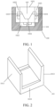
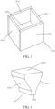
- the pixel units each may include a base, the base being provided with an installation space; a photodiode, the photodiode being installed in the installation space, and the photodiode including a red photodiode, a green photodiode, and a blue photodiode that are spaced from each other; and an optical splitter, the optical splitter being installed on the base, at least part of the optical splitter being located in the installation space, the optical splitter having a light-in surface, a first light-out surface, a second light-out surface and a third light-out surface, and the optical splitter being configured to disperse light entering the light-in surface and then emit the light from the first light-out surface, the second light-out surface and the third light-
- light passing through the optical splitter is divided into three beams of light in different directions, which respectively enter the red photodiode, the green photodiode and the blue photodiode, so that the pixel unit can simultaneously acquire R, G and B signals, effectively eliminating the false color effects of the photoelectric sensor.
- the radio frequency unit 401 may be configured to receive and send a signal during an information receiving and sending process or a call process. Specifically, the radio frequency unit receives downlink data from a base station, then delivers the downlink information to the processor 410 for processing, and sends related uplink data to the base station.
- the radio frequency unit 401 includes, but is not limited to, an antenna, at least one amplifier, a transceiver, a coupler, a low noise amplifier, a duplexer, and the like.
- the radio frequency unit 401 may further communicate with the network and another device through wireless communication system.
- the electronic device provides the user with wireless broadband Internet access in a network module 402, such as helping the user to send and receive emails, browse web pages, and access streaming media.
- the audio output unit 403 may convert audio data received by the radio frequency unit 401 or the network module 402 or stored in the memory 409 into an audio signal and output the audio signal as sound.
- the audio output unit 403 may further provide an audio output that is related to a particular function executed by the electronic device 400 (for example, a call signal receiving sound or a message receiving sound).
- the audio output unit 403 includes a speaker, a buzzer, a receiver, and the like.
- the input unit 404 is configured to receive an audio or video signal.
- the input unit 404 may include a graphics processing unit (Graphics Processing Unit, GPU) 4041 and a microphone 4042.
- the graphics processing unit 4041 performs processing on image data of a static picture or a video that is obtained by an image acquisition device (for example, a camera) in a video acquisition mode or an image acquisition mode.
- the processed image frame can be displayed on the display unit 406.
- An image frame that has been processed by the graphics processing unit 4041 may be stored in the memory 409 (or another storage medium) or sent by using the radio frequency unit 401 or the network module 402.
- the microphone 4042 may receive a sound, and can process the sound into audio data.
- the processed audio data may be transferred, in a phone talk mode, to a format that may be sent to a mobile communication base station via the radio frequency unit 401 to output.
- the electronic device 400 further includes at least one sensor 405, such as an optical sensor, a motion sensor, and other sensors.
- the optical sensor includes an ambient light sensor and a proximity sensor, where the ambient light sensor may adjust luminance of the display panel 4061 according to the luminance of the ambient light, and the proximity sensor may switch off the display panel 4061 and/or backlight when the electronic device 400 is moved to the ear.
- an acceleration sensor may detect magnitude of accelerations in various directions (which generally are triaxial), may detect magnitude and a direction of the gravity when static, and may be configured to identify an electronic device gesture (such as switchover between horizontal and vertical screens, a related game, and gesture calibration of a magnetometer), a related function of vibration identification (such as a pedometer and a knock).
- the sensor 405 may also include a fingerprint sensor, a pressure sensor, an iris sensor, a molecular sensor, a gyroscope, a barometer, a hygrometer, a thermometer, an infrared sensor, and the like, which are not be described herein again.
- the display unit 406 is configured to display information input by the user or information provided for the user.
- the display unit 406 may include a display panel 4061, and the display panel 4061 may be configured by using a liquid crystal display (liquid crystal display, LCD), an organic light-emitting diode (organic light-emitting diode, OLED), or the like.
- the user input unit 407 may be configured to receive input digit or character information, and generate key signal input related to the user setting and function control of the electronic device.
- the user input unit 407 includes a touch panel 4071 and another input device 4072.
- the touch panel 4071 also referred to as a touchscreen, may collect a touch operation of a user on or near the touch panel (such as an operation by a user on or near the touch panel 4071 by using any suitable object or attachment, such as a finger or a touch pen).
- the touch panel 4071 may include two parts: a touch detection apparatus and a touch controller.
- the touch detection apparatus detects a touch position of the user, detects a signal generated by the touch operation, and transfers the signal to the touch controller.
- the touch controller receives the touch information from the touch detection apparatus, converts the touch information into touch point coordinates, sends the touch point coordinates to the processor 410, and receives and executes a command sent from the processor 410.
- the touch panel 4071 may be implemented by using various types, such as a resistive type, a capacitive type, an infrared type, and a surface acoustic wave type.
- the user input unit 407 may further include the another input device 4072.
- the another input device 4072 may include, but is not limited to, a physical keyboard, a functional key (such as a volume control key or a switch key), a track ball, a mouse, and a joystick, which are not repeated herein.
- the touch panel 4071 may cover the display panel 4061. After detecting a touch operation on or near the touch panel, the touch panel 4071 transfers the touch operation to the processor 410, to determine a type of a touch event. Then, the processor 410 provides a corresponding visual output on the display panel 4061 according to the type of the touch event.
- the touch panel 4071 and the display panel 4061 implement, as two independent parts, input and output functions of the electronic device. However, in some embodiments, the touch panel 4071 and the display panel 4061 may be integrated to implement the input and output functions of the electronic device, which is not specifically limited herein.
- the interface unit 408 is an interface for connecting an external apparatus to the electronic device 400.
- the external apparatus may include a wired or wireless headset port, an external power supply (or battery charger) port, a wired or wireless data port, a memory card port, a port for connecting an apparatus with a recognition module, an audio input/output (I/O) port, a video I/O port, a headphone port, and the like.
- the interface unit 408 may be configured to receive an input (for example, data information or power) from an external apparatus, and transmit the received input to one or more elements in the electronic device 400, or may be configured to transmit data between the electronic device 400 and the external apparatus.
- the memory 409 may be configured to store a software program and various data.
- the memory 409 may mainly include a program storage area and a data storage area.
- the program storage area may store an operating system, an application program required by at least one function (for example, a sound playback function and an image display function), and the like.
- the data storage area may store data (for example, audio data and an address book) created according to the use of the mobile phone, and the like.
- the memory 409 may include a high-speed random access memory, and may also include a nonvolatile memory, for example, at least one magnetic disk storage device, a flash memory, or another volatile solid-state storage device.
- the processor 410 is a control center of the electronic device, and connects various parts of the entire electronic device by using various interfaces and lines. By running or executing the software program and/or module stored in the memory 409, and invoking data stored in the memory 409, the processor 410 performs various functions of the electronic device and processes data, thereby performing overall monitoring on the electronic device.
- the processor 410 may include one or more processing units.
- the processor 410 may integrate an application processor and a modem processor.
- the application processor mainly processes an operating system, a user interface, an application program, and the like.
- the modem processor mainly processes wireless communication. It may be understood that, the modem processor may alternatively not be integrated in the processor 410.
- the electronic device 400 may further include the power supply 411 (such as a battery) for supplying power to the components.
- the power supply 411 may logically connect to the processor 410 by using a power supply management system, thereby implementing functions, such as charging, discharging, and power consumption management, by using the power supply management system.
- the electronic device 400 includes some functional modules not shown, which are not described herein again.
- the embodiments of the present disclosure further provide an electronic device, including a processor 410, a memory 409, and a computer program on the memory 409 and executed on the processor 410, where when executed by the processor 410, the computer program implements the processes of the embodiments, and can achieve the same technical effects. To avoid repetition, details are not described herein again.
- the embodiments of the present disclosure may be provided as a method, a system, or a computer program product. Therefore, the present disclosure may use a form of hardware only embodiments, software only embodiments, or embodiments with a combination of software and hardware. Moreover, the present disclosure may use a form of a computer program product that is implemented on one or more computer-usable storage media (including but not limited to a disk memory, a CD-ROM, an optical memory, and the like) that include computer-usable program code.
- computer-usable storage media including but not limited to a disk memory, a CD-ROM, an optical memory, and the like
- These computer program instructions may be provided to a general-purpose computer, a special-purpose computer, an embedded processor, or a processor of another programmable data processing device to generate a machine, so that an apparatus configured to implement functions specified in one or more procedures in the flowcharts and/or one or more blocks in the block diagrams is generated by using instructions executed by the general-purpose computer or the processor of another programmable data processing device.
- These computer program instructions may also be stored in a computer readable memory that can instruct a computer or any other programmable data processing device to work in a specific manner, so that the instructions stored in the computer readable memory generate an artifact that includes an instruction apparatus.
- the instruction apparatus implements a specific function in one or more processes in the flowcharts and/or in one or more blocks in the block diagrams.
- These computer program instructions may also be loaded onto a computer or another programmable data processing device, so that a series of operations and steps are performed on the computer or the another programmable device, thereby generating computer-implemented processing. Therefore, the instructions executed on the computer or the another programmable device provide steps for implementing a specific function in one or more processes in the flowcharts and/or in one or more blocks in the schematic structural diagrams.
- a computing device includes one or more processors (CPUs), an input/output interface, a network interface, and an internal memory.
- processors CPUs
- input/output interface input/output interface
- network interface network interface
- internal memory volatile and non-volatile memory
- the memory may include a form such as a volatile memory, a random-access memory (RAM) and/or a non-volatile memory such as a read-only memory (ROM) or a flash RAM in a computer-readable medium.
- RAM random-access memory
- ROM read-only memory
- flash RAM flash RAM
- the memory is an example of the computer-readable medium.
Landscapes
- Physics & Mathematics (AREA)
- Engineering & Computer Science (AREA)
- Multimedia (AREA)
- Signal Processing (AREA)
- General Physics & Mathematics (AREA)
- Optics & Photonics (AREA)
- Spectroscopy & Molecular Physics (AREA)
- Color Television Image Signal Generators (AREA)
- Transforming Light Signals Into Electric Signals (AREA)
Claims (10)
- Pixeleinheit (100), umfassend:eine Basis, wobei die Basis mit einem Installationsraum versehen ist;eine Photodiode, wobei die Photodiode in dem Installationsraum installiert ist und die Photodiode eine rote Photodiode (1021), eine grüne Photodiode (1022) und eine blaue Photodiode (1023) umfasst, die voneinander beabstandet sind; undeinen optischen Splitter (103), wobei der optische Splitter (103) auf der Basis installiert ist, wobei sich zumindest ein Teil des optischen Splitters (103) im Installationsraum befindet, wobei der optische Splitter (103) eine Einleuchtfläche (1031), eine erste Ausleuchtfläche (1032), eine zweite Ausleuchtfläche (1033) und eine dritte Ausleuchtfläche (1034) aufweist, und wobei der optische Splitter (103) konfiguriert ist, um Licht, das in die Einleuchtfläche (1031) eintritt, zu zerstreuen und dann das Licht von der ersten Ausleuchtfläche (1032), der zweiten Ausleuchtfläche (1033) und der dritten Ausleuchtfläche (1034) zu emittieren, wobei die erste Ausleuchtfläche (1032) der roten Photodiode (1021) zugewandt ist, die zweite Ausleuchtfläche (1033) der grünen Photodiode (1022) zugewandt ist und die dritte Ausleuchtfläche (1034) der blauen Photodiode (1023) zugewandt ist,wobei die Basis Folgendes umfasst:eine Bodenplatte (1010), eine erstes Seitenpaneel (1011), ein zweites Seitenpaneel (1012), ein drittes Seitenpaneel (1013) und ein viertes Seitenpaneel (1014),wobei das erste Seitenpaneel (1011), das zweite Seitenpaneel (1012), das dritte Seitenpaneel (1013) und das vierte Seitenpaneel (1014) nacheinander ringförmig verbunden sind und das erste Seitenpaneel (1011), das zweite Seitenpaneel (1012), das dritte Seitenpaneel (1013) und das vierte Seitenpaneel (1014) jeweils mit Kanten der Bodenplatte (1010) verbunden sind, der Installationsraum zwischen der Bodenplatte (1010), dem ersten Seitenpaneel (1011), dem zweiten Seitenpaneel (1012), dem dritten Seitenpaneel (1013) und dem vierten Seitenpaneel (1014) gebildet ist und die Photodiode und der optische Splitter (103) beide in den Installationsraum installiert sind,dadurch gekennzeichnet, dassdie Bodenplatte (1010), das erste Seitenpaneel (1011) und das dritte Seitenpaneel (1013) jeweils mit einer der roten Photodiode (1021), der grünen Photodiode (1022) und der blauen Photodiode (1023) versehen sind.
- Pixeleinheit (100) nach Anspruch 1, wobei ein Querschnitt des optischen Splitters (103) die Form eines Trapezes aufweist, eine Fläche, in der sich eine Basis des Trapezes befindet, die Einleuchtfläche (1031) bildet, und eine Fläche, in der sich die andere Basis des Trapezes befindet, und Flächen, in denen sich zwei Schenkel des Trapezes befinden, jeweils eine von der ersten Ausleuchtfläche (1032), der zweiten Ausleuchtfläche (1033) und der dritten Ausleuchtfläche (1034) bilden.
- Pixeleinheit (100) nach Anspruch 2, wobei der Installationsraum eine Lichtdurchlassöffnung aufweist, die mit der Außenseite kommuniziert, der optische Splitter (103) in dem Installationsraum installiert ist und der Querschnitt des optischen Splitters (103) die Form eines gleichschenkligen Trapezes aufweist, wobei das gleichschenklige Trapez eine untere Basis aufweist, die der Lichtdurchlassöffnung zugewandt ist.
- Pixeleinheit (100) nach Anspruch 1, wobei die Basis ein Silikonelement ist.
- Photoelektrischer Sensor (200), dadurch gekennzeichnet, dass der photoelektrische Sensor Folgendes umfasst:eine Pixeleinheit (100), wobei die Pixeleinheit (100) die Pixeleinheit (100) nach einem der Ansprüche 1 bis 4 ist; undeine lichtempfindliche Steuerschaltung, wobei die lichtempfindliche Steuerschaltung eine erste lichtempfindliche Steuerschaltung, eine zweite lichtempfindliche Steuerschaltung und eine dritte lichtempfindliche Steuerschaltung umfasst, wobei die rote Photodiode (1021), die grüne Photodiode (1022) und die blaue Photodiode (1023) jeweils mit der ersten lichtempfindlichen Steuerschaltung, der zweiten lichtempfindlichen Steuerschaltung und der dritten lichtempfindlichen Steuerschaltung verbunden sind, um jeweils empfangene optische Signale in elektrische Signale umzuwandeln.
- Photoelektrischer Sensor (200) nach Anspruch 5, wobei die lichtempfindliche Steuerschaltung auf der Basis angeordnet ist.
- Photoelektrischer Sensor (200) nach Anspruch 5, wobei der photoelektrische Sensor (200) eine Vielzahl von Pixeleinheiten (100) umfasst, wobei die Vielzahl von Pixeleinheiten (100) in einem Array verbunden und angeordnet ist.
- Photoelektrischer Sensor (200) nach Anspruch 7, wobei benachbarte Pixeleinheiten (100) die Basis teilen.
- Kameramodul, umfassend: eine Leiterplatte (305), eine Linse (301) und einen photoelektrischen Sensor (200), wobei der photoelektrische Sensor (200) auf der Leiterplatte (305) installiert und elektrisch mit der Leiterplatte (305) verbunden ist,dadurch gekennzeichnet, dass der photoelektrische Sensor (200) der photoelektrische Sensor (200) nach Anspruch 5 oder 6 ist; unddie Linse (301) auf einer Seite des photoelektrischen Sensors (200) entfernt von der Leiterplatte (305) angeordnet ist.
- Elektronische Vorrichtung, umfassend das Kameramodul nach Anspruch 9.
Applications Claiming Priority (2)
| Application Number | Priority Date | Filing Date | Title |
|---|---|---|---|
| CN202010456160.2A CN111614878B (zh) | 2020-05-26 | 2020-05-26 | 像素单元、光电传感器、摄像模组及电子设备 |
| PCT/CN2021/095530 WO2021238869A1 (zh) | 2020-05-26 | 2021-05-24 | 像素单元、光电传感器、摄像模组及电子设备 |
Publications (3)
| Publication Number | Publication Date |
|---|---|
| EP4161052A1 EP4161052A1 (de) | 2023-04-05 |
| EP4161052A4 EP4161052A4 (de) | 2024-03-20 |
| EP4161052B1 true EP4161052B1 (de) | 2025-07-09 |
Family
ID=72203240
Family Applications (1)
| Application Number | Title | Priority Date | Filing Date |
|---|---|---|---|
| EP21812616.7A Active EP4161052B1 (de) | 2020-05-26 | 2021-05-24 | Pixeleinheit, photoelektrischer sensor, kameramodul und elektronische vorrichtung |
Country Status (7)
| Country | Link |
|---|---|
| US (1) | US12063424B2 (de) |
| EP (1) | EP4161052B1 (de) |
| JP (1) | JP7450070B2 (de) |
| KR (1) | KR102736556B1 (de) |
| CN (1) | CN111614878B (de) |
| ES (1) | ES3037554T3 (de) |
| WO (1) | WO2021238869A1 (de) |
Families Citing this family (2)
| Publication number | Priority date | Publication date | Assignee | Title |
|---|---|---|---|---|
| CN111614878B (zh) | 2020-05-26 | 2022-04-22 | 维沃移动通信(杭州)有限公司 | 像素单元、光电传感器、摄像模组及电子设备 |
| CN114422730B (zh) * | 2022-01-17 | 2024-03-19 | 惠州Tcl移动通信有限公司 | 图像传感器及电子设备 |
Family Cites Families (16)
| Publication number | Priority date | Publication date | Assignee | Title |
|---|---|---|---|---|
| US5340978A (en) * | 1992-09-30 | 1994-08-23 | Lsi Logic Corporation | Image-sensing display panels with LCD display panel and photosensitive element array |
| JPH11313334A (ja) * | 1998-04-27 | 1999-11-09 | Nippon Hoso Kyokai <Nhk> | 固体撮像装置 |
| JP2000151933A (ja) * | 1998-11-06 | 2000-05-30 | Nec Corp | 撮像素子及びその製造方法 |
| US6882367B1 (en) * | 2000-02-29 | 2005-04-19 | Foveon, Inc. | High-sensitivity storage pixel sensor having auto-exposure detection |
| JP2001309395A (ja) * | 2000-04-21 | 2001-11-02 | Sony Corp | 固体撮像素子及びその製造方法 |
| US8599301B2 (en) * | 2006-04-17 | 2013-12-03 | Omnivision Technologies, Inc. | Arrayed imaging systems having improved alignment and associated methods |
| US20090096900A1 (en) * | 2007-10-11 | 2009-04-16 | Chin-Poh Pang | Image sensor device |
| CN102160180A (zh) * | 2009-07-24 | 2011-08-17 | 松下电器产业株式会社 | 摄像装置以及固体摄像元件 |
| US8792027B2 (en) * | 2010-01-06 | 2014-07-29 | Panasonic Corporation | Solid-state image pickup device, imaging device, and dispersing element |
| CN102510447B (zh) * | 2011-09-28 | 2016-08-10 | 上海华虹宏力半导体制造有限公司 | 图像传感器 |
| KR102724720B1 (ko) * | 2016-12-28 | 2024-11-01 | 삼성전자주식회사 | 광센서 |
| CN107613182A (zh) * | 2017-10-27 | 2018-01-19 | 北京小米移动软件有限公司 | 摄像头感光组件、摄像头和摄像终端 |
| KR102424652B1 (ko) * | 2017-11-17 | 2022-07-25 | 삼성전자주식회사 | 이미지 센서 |
| CN107861242B (zh) * | 2017-12-20 | 2019-07-05 | 嘉兴中润光学科技有限公司 | 具有多传感器的成像系统 |
| CN110858584A (zh) * | 2018-08-23 | 2020-03-03 | 弘凯光电(深圳)有限公司 | 发光模块及发光串列装置 |
| CN111614878B (zh) * | 2020-05-26 | 2022-04-22 | 维沃移动通信(杭州)有限公司 | 像素单元、光电传感器、摄像模组及电子设备 |
-
2020
- 2020-05-26 CN CN202010456160.2A patent/CN111614878B/zh active Active
-
2021
- 2021-05-24 JP JP2022571284A patent/JP7450070B2/ja active Active
- 2021-05-24 KR KR1020227045489A patent/KR102736556B1/ko active Active
- 2021-05-24 EP EP21812616.7A patent/EP4161052B1/de active Active
- 2021-05-24 ES ES21812616T patent/ES3037554T3/es active Active
- 2021-05-24 WO PCT/CN2021/095530 patent/WO2021238869A1/zh not_active Ceased
-
2022
- 2022-11-23 US US17/993,862 patent/US12063424B2/en active Active
Also Published As
| Publication number | Publication date |
|---|---|
| ES3037554T3 (en) | 2025-10-03 |
| JP7450070B2 (ja) | 2024-03-14 |
| JP2023526971A (ja) | 2023-06-26 |
| WO2021238869A1 (zh) | 2021-12-02 |
| US20230100569A1 (en) | 2023-03-30 |
| KR20230016664A (ko) | 2023-02-02 |
| EP4161052A1 (de) | 2023-04-05 |
| US12063424B2 (en) | 2024-08-13 |
| KR102736556B1 (ko) | 2024-12-02 |
| CN111614878A (zh) | 2020-09-01 |
| CN111614878B (zh) | 2022-04-22 |
| EP4161052A4 (de) | 2024-03-20 |
Similar Documents
| Publication | Publication Date | Title |
|---|---|---|
| US12003860B2 (en) | Image processing method and electronic device | |
| US11962918B2 (en) | Image sensor, mobile terminal, and image photographing method | |
| US20210144323A1 (en) | Image sensor and mobile terminal | |
| EP3709625B1 (de) | Kameraanordnung, bildaufnahmeverfahren und mobiles endgerät | |
| EP3826285B1 (de) | Bildsensor, mobiles terminal, und fotografieverfahren | |
| CN108965666B (zh) | 一种移动终端及图像拍摄方法 | |
| US20100238184A1 (en) | Method and apparatus for three-dimensional visualization in mobile devices | |
| US12063424B2 (en) | Pixel unit, photoelectric sensor, camera module and electronic device | |
| CN107895352A (zh) | 一种图像处理方法及移动终端 | |
| US20240014236A9 (en) | Mobile terminal and image photographing method | |
| US11996421B2 (en) | Image sensor, mobile terminal, and image capturing method | |
| CN110798601A (zh) | 摄像模组、电子设备、拍摄控制方法及装置 | |
| US20220201223A1 (en) | Image processing method, electronic device and medium | |
| CN214591630U (zh) | 潜望摄像模组及移动终端 | |
| CN213750591U (zh) | 背光模组、显示装置及移动终端 | |
| CN110248050B (zh) | 一种摄像头模组及移动终端 | |
| CN217508882U (zh) | 摄像装置及移动终端 | |
| CN213028136U (zh) | 移动终端 | |
| CN213028135U (zh) | 移动终端 | |
| CN115225789A (zh) | 感光模组、图像获取设备、图像获取方法及智能终端 |
Legal Events
| Date | Code | Title | Description |
|---|---|---|---|
| STAA | Information on the status of an ep patent application or granted ep patent |
Free format text: STATUS: THE INTERNATIONAL PUBLICATION HAS BEEN MADE |
|
| PUAI | Public reference made under article 153(3) epc to a published international application that has entered the european phase |
Free format text: ORIGINAL CODE: 0009012 |
|
| STAA | Information on the status of an ep patent application or granted ep patent |
Free format text: STATUS: REQUEST FOR EXAMINATION WAS MADE |
|
| 17P | Request for examination filed |
Effective date: 20221220 |
|
| AK | Designated contracting states |
Kind code of ref document: A1 Designated state(s): AL AT BE BG CH CY CZ DE DK EE ES FI FR GB GR HR HU IE IS IT LI LT LU LV MC MK MT NL NO PL PT RO RS SE SI SK SM TR |
|
| DAV | Request for validation of the european patent (deleted) | ||
| DAX | Request for extension of the european patent (deleted) | ||
| REG | Reference to a national code |
Ref legal event code: R079 Ref country code: DE Ref legal event code: R079 Ref document number: 602021033904 Country of ref document: DE Free format text: PREVIOUS MAIN CLASS: H04N0005225000 Ipc: H01L0027146000 |
|
| A4 | Supplementary search report drawn up and despatched |
Effective date: 20240221 |
|
| RIC1 | Information provided on ipc code assigned before grant |
Ipc: H01L 27/146 20060101AFI20240215BHEP |
|
| REG | Reference to a national code |
Ref country code: DE Ref legal event code: R079 Free format text: PREVIOUS MAIN CLASS: H01L0027146000 Ipc: H10F0039000000 Ref country code: DE Ref legal event code: R079 Ref document number: 602021033904 Country of ref document: DE Free format text: PREVIOUS MAIN CLASS: H01L0027146000 Ipc: H10F0039000000 |
|
| GRAP | Despatch of communication of intention to grant a patent |
Free format text: ORIGINAL CODE: EPIDOSNIGR1 |
|
| STAA | Information on the status of an ep patent application or granted ep patent |
Free format text: STATUS: GRANT OF PATENT IS INTENDED |
|
| RIC1 | Information provided on ipc code assigned before grant |
Ipc: H10F 39/00 20250101AFI20250304BHEP |
|
| INTG | Intention to grant announced |
Effective date: 20250318 |
|
| GRAS | Grant fee paid |
Free format text: ORIGINAL CODE: EPIDOSNIGR3 |
|
| GRAA | (expected) grant |
Free format text: ORIGINAL CODE: 0009210 |
|
| STAA | Information on the status of an ep patent application or granted ep patent |
Free format text: STATUS: THE PATENT HAS BEEN GRANTED |
|
| AK | Designated contracting states |
Kind code of ref document: B1 Designated state(s): AL AT BE BG CH CY CZ DE DK EE ES FI FR GB GR HR HU IE IS IT LI LT LU LV MC MK MT NL NO PL PT RO RS SE SI SK SM TR |
|
| REG | Reference to a national code |
Ref country code: GB Ref legal event code: FG4D |
|
| REG | Reference to a national code |
Ref country code: CH Ref legal event code: EP |
|
| REG | Reference to a national code |
Ref country code: IE Ref legal event code: FG4D |
|
| REG | Reference to a national code |
Ref country code: DE Ref legal event code: R096 Ref document number: 602021033904 Country of ref document: DE |
|
| REG | Reference to a national code |
Ref country code: NL Ref legal event code: FP |
|
| REG | Reference to a national code |
Ref country code: ES Ref legal event code: FG2A Ref document number: 3037554 Country of ref document: ES Kind code of ref document: T3 Effective date: 20251003 |
|
| PG25 | Lapsed in a contracting state [announced via postgrant information from national office to epo] |
Ref country code: PT Free format text: LAPSE BECAUSE OF FAILURE TO SUBMIT A TRANSLATION OF THE DESCRIPTION OR TO PAY THE FEE WITHIN THE PRESCRIBED TIME-LIMIT Effective date: 20251110 |
|
| REG | Reference to a national code |
Ref country code: AT Ref legal event code: MK05 Ref document number: 1813122 Country of ref document: AT Kind code of ref document: T Effective date: 20250709 |
|
| PG25 | Lapsed in a contracting state [announced via postgrant information from national office to epo] |
Ref country code: IS Free format text: LAPSE BECAUSE OF FAILURE TO SUBMIT A TRANSLATION OF THE DESCRIPTION OR TO PAY THE FEE WITHIN THE PRESCRIBED TIME-LIMIT Effective date: 20251109 |
|
| PG25 | Lapsed in a contracting state [announced via postgrant information from national office to epo] |
Ref country code: NO Free format text: LAPSE BECAUSE OF FAILURE TO SUBMIT A TRANSLATION OF THE DESCRIPTION OR TO PAY THE FEE WITHIN THE PRESCRIBED TIME-LIMIT Effective date: 20251009 |
|
| REG | Reference to a national code |
Ref country code: LT Ref legal event code: MG9D |
|
| PG25 | Lapsed in a contracting state [announced via postgrant information from national office to epo] |
Ref country code: AT Free format text: LAPSE BECAUSE OF FAILURE TO SUBMIT A TRANSLATION OF THE DESCRIPTION OR TO PAY THE FEE WITHIN THE PRESCRIBED TIME-LIMIT Effective date: 20250709 |
|
| PG25 | Lapsed in a contracting state [announced via postgrant information from national office to epo] |
Ref country code: FI Free format text: LAPSE BECAUSE OF FAILURE TO SUBMIT A TRANSLATION OF THE DESCRIPTION OR TO PAY THE FEE WITHIN THE PRESCRIBED TIME-LIMIT Effective date: 20250709 |
|
| PG25 | Lapsed in a contracting state [announced via postgrant information from national office to epo] |
Ref country code: HR Free format text: LAPSE BECAUSE OF FAILURE TO SUBMIT A TRANSLATION OF THE DESCRIPTION OR TO PAY THE FEE WITHIN THE PRESCRIBED TIME-LIMIT Effective date: 20250709 |
|
| PG25 | Lapsed in a contracting state [announced via postgrant information from national office to epo] |
Ref country code: GR Free format text: LAPSE BECAUSE OF FAILURE TO SUBMIT A TRANSLATION OF THE DESCRIPTION OR TO PAY THE FEE WITHIN THE PRESCRIBED TIME-LIMIT Effective date: 20251010 |
|
| PG25 | Lapsed in a contracting state [announced via postgrant information from national office to epo] |
Ref country code: SE Free format text: LAPSE BECAUSE OF FAILURE TO SUBMIT A TRANSLATION OF THE DESCRIPTION OR TO PAY THE FEE WITHIN THE PRESCRIBED TIME-LIMIT Effective date: 20250709 |
|
| PG25 | Lapsed in a contracting state [announced via postgrant information from national office to epo] |
Ref country code: LV Free format text: LAPSE BECAUSE OF FAILURE TO SUBMIT A TRANSLATION OF THE DESCRIPTION OR TO PAY THE FEE WITHIN THE PRESCRIBED TIME-LIMIT Effective date: 20250709 |
|
| PG25 | Lapsed in a contracting state [announced via postgrant information from national office to epo] |
Ref country code: BG Free format text: LAPSE BECAUSE OF FAILURE TO SUBMIT A TRANSLATION OF THE DESCRIPTION OR TO PAY THE FEE WITHIN THE PRESCRIBED TIME-LIMIT Effective date: 20250709 Ref country code: PL Free format text: LAPSE BECAUSE OF FAILURE TO SUBMIT A TRANSLATION OF THE DESCRIPTION OR TO PAY THE FEE WITHIN THE PRESCRIBED TIME-LIMIT Effective date: 20250709 |
|
| PG25 | Lapsed in a contracting state [announced via postgrant information from national office to epo] |
Ref country code: RS Free format text: LAPSE BECAUSE OF FAILURE TO SUBMIT A TRANSLATION OF THE DESCRIPTION OR TO PAY THE FEE WITHIN THE PRESCRIBED TIME-LIMIT Effective date: 20251009 |
|
| PG25 | Lapsed in a contracting state [announced via postgrant information from national office to epo] |
Ref country code: SM Free format text: LAPSE BECAUSE OF FAILURE TO SUBMIT A TRANSLATION OF THE DESCRIPTION OR TO PAY THE FEE WITHIN THE PRESCRIBED TIME-LIMIT Effective date: 20250709 |
|
| PGFP | Annual fee paid to national office [announced via postgrant information from national office to epo] |
Ref country code: GB Payment date: 20260324 Year of fee payment: 6 |
|
| PG25 | Lapsed in a contracting state [announced via postgrant information from national office to epo] |
Ref country code: DK Free format text: LAPSE BECAUSE OF FAILURE TO SUBMIT A TRANSLATION OF THE DESCRIPTION OR TO PAY THE FEE WITHIN THE PRESCRIBED TIME-LIMIT Effective date: 20250709 |
|
| PG25 | Lapsed in a contracting state [announced via postgrant information from national office to epo] |
Ref country code: CZ Free format text: LAPSE BECAUSE OF FAILURE TO SUBMIT A TRANSLATION OF THE DESCRIPTION OR TO PAY THE FEE WITHIN THE PRESCRIBED TIME-LIMIT Effective date: 20250709 |
|
| PG25 | Lapsed in a contracting state [announced via postgrant information from national office to epo] |
Ref country code: EE Free format text: LAPSE BECAUSE OF FAILURE TO SUBMIT A TRANSLATION OF THE DESCRIPTION OR TO PAY THE FEE WITHIN THE PRESCRIBED TIME-LIMIT Effective date: 20250709 Ref country code: SK Free format text: LAPSE BECAUSE OF FAILURE TO SUBMIT A TRANSLATION OF THE DESCRIPTION OR TO PAY THE FEE WITHIN THE PRESCRIBED TIME-LIMIT Effective date: 20250709 |
|
| PLBE | No opposition filed within time limit |
Free format text: ORIGINAL CODE: 0009261 |
|
| STAA | Information on the status of an ep patent application or granted ep patent |
Free format text: STATUS: NO OPPOSITION FILED WITHIN TIME LIMIT |