EP4155866B1 - Faltbare anzeigetafel mit einer einziehbaren transparenten displayabdeckung - Google Patents
Faltbare anzeigetafel mit einer einziehbaren transparenten displayabdeckung Download PDFInfo
- Publication number
- EP4155866B1 EP4155866B1 EP22193444.1A EP22193444A EP4155866B1 EP 4155866 B1 EP4155866 B1 EP 4155866B1 EP 22193444 A EP22193444 A EP 22193444A EP 4155866 B1 EP4155866 B1 EP 4155866B1
- Authority
- EP
- European Patent Office
- Prior art keywords
- panel area
- scan
- panel
- sub
- area
- Prior art date
- Legal status (The legal status is an assumption and is not a legal conclusion. Google has not performed a legal analysis and makes no representation as to the accuracy of the status listed.)
- Active
Links
Images







Classifications
-
- G—PHYSICS
- G06—COMPUTING OR CALCULATING; COUNTING
- G06F—ELECTRIC DIGITAL DATA PROCESSING
- G06F1/00—Details not covered by groups G06F3/00 - G06F13/00 and G06F21/00
- G06F1/16—Constructional details or arrangements
- G06F1/1601—Constructional details related to the housing of computer displays, e.g. of CRT monitors, of flat displays
- G06F1/1605—Multimedia displays, e.g. with integrated or attached speakers, cameras, microphones
-
- G—PHYSICS
- G06—COMPUTING OR CALCULATING; COUNTING
- G06F—ELECTRIC DIGITAL DATA PROCESSING
- G06F1/00—Details not covered by groups G06F3/00 - G06F13/00 and G06F21/00
- G06F1/16—Constructional details or arrangements
- G06F1/1613—Constructional details or arrangements for portable computers
- G06F1/1615—Constructional details or arrangements for portable computers with several enclosures having relative motions, each enclosure supporting at least one I/O or computing function
- G06F1/1616—Constructional details or arrangements for portable computers with several enclosures having relative motions, each enclosure supporting at least one I/O or computing function with folding flat displays, e.g. laptop computers or notebooks having a clamshell configuration, with body parts pivoting to an open position around an axis parallel to the plane they define in closed position
-
- G—PHYSICS
- G06—COMPUTING OR CALCULATING; COUNTING
- G06F—ELECTRIC DIGITAL DATA PROCESSING
- G06F1/00—Details not covered by groups G06F3/00 - G06F13/00 and G06F21/00
- G06F1/16—Constructional details or arrangements
- G06F1/1613—Constructional details or arrangements for portable computers
- G06F1/1615—Constructional details or arrangements for portable computers with several enclosures having relative motions, each enclosure supporting at least one I/O or computing function
- G06F1/1624—Constructional details or arrangements for portable computers with several enclosures having relative motions, each enclosure supporting at least one I/O or computing function with sliding enclosures, e.g. sliding keyboard or display
-
- G—PHYSICS
- G06—COMPUTING OR CALCULATING; COUNTING
- G06F—ELECTRIC DIGITAL DATA PROCESSING
- G06F1/00—Details not covered by groups G06F3/00 - G06F13/00 and G06F21/00
- G06F1/16—Constructional details or arrangements
- G06F1/1613—Constructional details or arrangements for portable computers
- G06F1/1633—Constructional details or arrangements of portable computers not specific to the type of enclosures covered by groups G06F1/1615 - G06F1/1626
- G06F1/1637—Details related to the display arrangement, including those related to the mounting of the display in the housing
- G06F1/1641—Details related to the display arrangement, including those related to the mounting of the display in the housing the display being formed by a plurality of foldable display components
-
- G—PHYSICS
- G06—COMPUTING OR CALCULATING; COUNTING
- G06F—ELECTRIC DIGITAL DATA PROCESSING
- G06F1/00—Details not covered by groups G06F3/00 - G06F13/00 and G06F21/00
- G06F1/16—Constructional details or arrangements
- G06F1/1613—Constructional details or arrangements for portable computers
- G06F1/1633—Constructional details or arrangements of portable computers not specific to the type of enclosures covered by groups G06F1/1615 - G06F1/1626
- G06F1/1637—Details related to the display arrangement, including those related to the mounting of the display in the housing
- G06F1/1643—Details related to the display arrangement, including those related to the mounting of the display in the housing the display being associated to a digitizer, e.g. laptops that can be used as penpads
-
- G—PHYSICS
- G06—COMPUTING OR CALCULATING; COUNTING
- G06F—ELECTRIC DIGITAL DATA PROCESSING
- G06F1/00—Details not covered by groups G06F3/00 - G06F13/00 and G06F21/00
- G06F1/16—Constructional details or arrangements
- G06F1/1613—Constructional details or arrangements for portable computers
- G06F1/1633—Constructional details or arrangements of portable computers not specific to the type of enclosures covered by groups G06F1/1615 - G06F1/1626
- G06F1/1637—Details related to the display arrangement, including those related to the mounting of the display in the housing
- G06F1/1652—Details related to the display arrangement, including those related to the mounting of the display in the housing the display being flexible, e.g. mimicking a sheet of paper, or rollable
-
- G—PHYSICS
- G06—COMPUTING OR CALCULATING; COUNTING
- G06F—ELECTRIC DIGITAL DATA PROCESSING
- G06F1/00—Details not covered by groups G06F3/00 - G06F13/00 and G06F21/00
- G06F1/16—Constructional details or arrangements
- G06F1/1613—Constructional details or arrangements for portable computers
- G06F1/1633—Constructional details or arrangements of portable computers not specific to the type of enclosures covered by groups G06F1/1615 - G06F1/1626
- G06F1/1656—Details related to functional adaptations of the enclosure, e.g. to provide protection against EMI, shock, water, or to host detachable peripherals like a mouse or removable expansions units like PCMCIA cards, or to provide access to internal components for maintenance or to removable storage supports like CDs or DVDs, or to mechanically mount accessories
-
- G—PHYSICS
- G06—COMPUTING OR CALCULATING; COUNTING
- G06F—ELECTRIC DIGITAL DATA PROCESSING
- G06F1/00—Details not covered by groups G06F3/00 - G06F13/00 and G06F21/00
- G06F1/16—Constructional details or arrangements
- G06F1/1613—Constructional details or arrangements for portable computers
- G06F1/1633—Constructional details or arrangements of portable computers not specific to the type of enclosures covered by groups G06F1/1615 - G06F1/1626
- G06F1/1675—Miscellaneous details related to the relative movement between the different enclosures or enclosure parts
- G06F1/1681—Details related solely to hinges
-
- G—PHYSICS
- G06—COMPUTING OR CALCULATING; COUNTING
- G06F—ELECTRIC DIGITAL DATA PROCESSING
- G06F1/00—Details not covered by groups G06F3/00 - G06F13/00 and G06F21/00
- G06F1/16—Constructional details or arrangements
- G06F1/1613—Constructional details or arrangements for portable computers
- G06F1/1633—Constructional details or arrangements of portable computers not specific to the type of enclosures covered by groups G06F1/1615 - G06F1/1626
- G06F1/1684—Constructional details or arrangements related to integrated I/O peripherals not covered by groups G06F1/1635 - G06F1/1675
- G06F1/1686—Constructional details or arrangements related to integrated I/O peripherals not covered by groups G06F1/1635 - G06F1/1675 the I/O peripheral being an integrated camera
-
- G—PHYSICS
- G06—COMPUTING OR CALCULATING; COUNTING
- G06F—ELECTRIC DIGITAL DATA PROCESSING
- G06F1/00—Details not covered by groups G06F3/00 - G06F13/00 and G06F21/00
- G06F1/16—Constructional details or arrangements
- G06F1/1613—Constructional details or arrangements for portable computers
- G06F1/1633—Constructional details or arrangements of portable computers not specific to the type of enclosures covered by groups G06F1/1615 - G06F1/1626
- G06F1/1684—Constructional details or arrangements related to integrated I/O peripherals not covered by groups G06F1/1635 - G06F1/1675
- G06F1/1688—Constructional details or arrangements related to integrated I/O peripherals not covered by groups G06F1/1635 - G06F1/1675 the I/O peripheral being integrated loudspeakers
-
- G—PHYSICS
- G09—EDUCATION; CRYPTOGRAPHY; DISPLAY; ADVERTISING; SEALS
- G09G—ARRANGEMENTS OR CIRCUITS FOR CONTROL OF INDICATING DEVICES USING STATIC MEANS TO PRESENT VARIABLE INFORMATION
- G09G3/00—Control arrangements or circuits, of interest only in connection with visual indicators other than cathode-ray tubes
- G09G3/20—Control arrangements or circuits, of interest only in connection with visual indicators other than cathode-ray tubes for presentation of an assembly of a number of characters, e.g. a page, by composing the assembly by combination of individual elements arranged in a matrix no fixed position being assigned to or needed to be assigned to the individual characters or partial characters
- G09G3/22—Control arrangements or circuits, of interest only in connection with visual indicators other than cathode-ray tubes for presentation of an assembly of a number of characters, e.g. a page, by composing the assembly by combination of individual elements arranged in a matrix no fixed position being assigned to or needed to be assigned to the individual characters or partial characters using controlled light sources
- G09G3/30—Control arrangements or circuits, of interest only in connection with visual indicators other than cathode-ray tubes for presentation of an assembly of a number of characters, e.g. a page, by composing the assembly by combination of individual elements arranged in a matrix no fixed position being assigned to or needed to be assigned to the individual characters or partial characters using controlled light sources using electroluminescent panels
- G09G3/32—Control arrangements or circuits, of interest only in connection with visual indicators other than cathode-ray tubes for presentation of an assembly of a number of characters, e.g. a page, by composing the assembly by combination of individual elements arranged in a matrix no fixed position being assigned to or needed to be assigned to the individual characters or partial characters using controlled light sources using electroluminescent panels semiconductive, e.g. using light-emitting diodes [LED]
- G09G3/3208—Control arrangements or circuits, of interest only in connection with visual indicators other than cathode-ray tubes for presentation of an assembly of a number of characters, e.g. a page, by composing the assembly by combination of individual elements arranged in a matrix no fixed position being assigned to or needed to be assigned to the individual characters or partial characters using controlled light sources using electroluminescent panels semiconductive, e.g. using light-emitting diodes [LED] organic, e.g. using organic light-emitting diodes [OLED]
- G09G3/3225—Control arrangements or circuits, of interest only in connection with visual indicators other than cathode-ray tubes for presentation of an assembly of a number of characters, e.g. a page, by composing the assembly by combination of individual elements arranged in a matrix no fixed position being assigned to or needed to be assigned to the individual characters or partial characters using controlled light sources using electroluminescent panels semiconductive, e.g. using light-emitting diodes [LED] organic, e.g. using organic light-emitting diodes [OLED] using an active matrix
- G09G3/3233—Control arrangements or circuits, of interest only in connection with visual indicators other than cathode-ray tubes for presentation of an assembly of a number of characters, e.g. a page, by composing the assembly by combination of individual elements arranged in a matrix no fixed position being assigned to or needed to be assigned to the individual characters or partial characters using controlled light sources using electroluminescent panels semiconductive, e.g. using light-emitting diodes [LED] organic, e.g. using organic light-emitting diodes [OLED] using an active matrix with pixel circuitry controlling the current through the light-emitting element
-
- G—PHYSICS
- G09—EDUCATION; CRYPTOGRAPHY; DISPLAY; ADVERTISING; SEALS
- G09G—ARRANGEMENTS OR CIRCUITS FOR CONTROL OF INDICATING DEVICES USING STATIC MEANS TO PRESENT VARIABLE INFORMATION
- G09G3/00—Control arrangements or circuits, of interest only in connection with visual indicators other than cathode-ray tubes
- G09G3/20—Control arrangements or circuits, of interest only in connection with visual indicators other than cathode-ray tubes for presentation of an assembly of a number of characters, e.g. a page, by composing the assembly by combination of individual elements arranged in a matrix no fixed position being assigned to or needed to be assigned to the individual characters or partial characters
- G09G3/22—Control arrangements or circuits, of interest only in connection with visual indicators other than cathode-ray tubes for presentation of an assembly of a number of characters, e.g. a page, by composing the assembly by combination of individual elements arranged in a matrix no fixed position being assigned to or needed to be assigned to the individual characters or partial characters using controlled light sources
- G09G3/30—Control arrangements or circuits, of interest only in connection with visual indicators other than cathode-ray tubes for presentation of an assembly of a number of characters, e.g. a page, by composing the assembly by combination of individual elements arranged in a matrix no fixed position being assigned to or needed to be assigned to the individual characters or partial characters using controlled light sources using electroluminescent panels
- G09G3/32—Control arrangements or circuits, of interest only in connection with visual indicators other than cathode-ray tubes for presentation of an assembly of a number of characters, e.g. a page, by composing the assembly by combination of individual elements arranged in a matrix no fixed position being assigned to or needed to be assigned to the individual characters or partial characters using controlled light sources using electroluminescent panels semiconductive, e.g. using light-emitting diodes [LED]
- G09G3/3208—Control arrangements or circuits, of interest only in connection with visual indicators other than cathode-ray tubes for presentation of an assembly of a number of characters, e.g. a page, by composing the assembly by combination of individual elements arranged in a matrix no fixed position being assigned to or needed to be assigned to the individual characters or partial characters using controlled light sources using electroluminescent panels semiconductive, e.g. using light-emitting diodes [LED] organic, e.g. using organic light-emitting diodes [OLED]
- G09G3/3266—Details of drivers for scan electrodes
-
- G—PHYSICS
- G09—EDUCATION; CRYPTOGRAPHY; DISPLAY; ADVERTISING; SEALS
- G09G—ARRANGEMENTS OR CIRCUITS FOR CONTROL OF INDICATING DEVICES USING STATIC MEANS TO PRESENT VARIABLE INFORMATION
- G09G3/00—Control arrangements or circuits, of interest only in connection with visual indicators other than cathode-ray tubes
- G09G3/20—Control arrangements or circuits, of interest only in connection with visual indicators other than cathode-ray tubes for presentation of an assembly of a number of characters, e.g. a page, by composing the assembly by combination of individual elements arranged in a matrix no fixed position being assigned to or needed to be assigned to the individual characters or partial characters
- G09G3/22—Control arrangements or circuits, of interest only in connection with visual indicators other than cathode-ray tubes for presentation of an assembly of a number of characters, e.g. a page, by composing the assembly by combination of individual elements arranged in a matrix no fixed position being assigned to or needed to be assigned to the individual characters or partial characters using controlled light sources
- G09G3/30—Control arrangements or circuits, of interest only in connection with visual indicators other than cathode-ray tubes for presentation of an assembly of a number of characters, e.g. a page, by composing the assembly by combination of individual elements arranged in a matrix no fixed position being assigned to or needed to be assigned to the individual characters or partial characters using controlled light sources using electroluminescent panels
- G09G3/32—Control arrangements or circuits, of interest only in connection with visual indicators other than cathode-ray tubes for presentation of an assembly of a number of characters, e.g. a page, by composing the assembly by combination of individual elements arranged in a matrix no fixed position being assigned to or needed to be assigned to the individual characters or partial characters using controlled light sources using electroluminescent panels semiconductive, e.g. using light-emitting diodes [LED]
- G09G3/3208—Control arrangements or circuits, of interest only in connection with visual indicators other than cathode-ray tubes for presentation of an assembly of a number of characters, e.g. a page, by composing the assembly by combination of individual elements arranged in a matrix no fixed position being assigned to or needed to be assigned to the individual characters or partial characters using controlled light sources using electroluminescent panels semiconductive, e.g. using light-emitting diodes [LED] organic, e.g. using organic light-emitting diodes [OLED]
- G09G3/3275—Details of drivers for data electrodes
-
- H—ELECTRICITY
- H05—ELECTRIC TECHNIQUES NOT OTHERWISE PROVIDED FOR
- H05K—PRINTED CIRCUITS; CASINGS OR CONSTRUCTIONAL DETAILS OF ELECTRIC APPARATUS; MANUFACTURE OF ASSEMBLAGES OF ELECTRICAL COMPONENTS
- H05K1/00—Printed circuits
- H05K1/18—Printed circuits structurally associated with non-printed electric components
- H05K1/189—Printed circuits structurally associated with non-printed electric components characterised by the use of flexible or folded printed circuits
-
- G—PHYSICS
- G09—EDUCATION; CRYPTOGRAPHY; DISPLAY; ADVERTISING; SEALS
- G09G—ARRANGEMENTS OR CIRCUITS FOR CONTROL OF INDICATING DEVICES USING STATIC MEANS TO PRESENT VARIABLE INFORMATION
- G09G2310/00—Command of the display device
- G09G2310/02—Addressing, scanning or driving the display screen or processing steps related thereto
- G09G2310/0264—Details of driving circuits
- G09G2310/0297—Special arrangements with multiplexing or demultiplexing of display data in the drivers for data electrodes, in a pre-processing circuitry delivering display data to said drivers or in the matrix panel, e.g. multiplexing plural data signals to one D/A converter or demultiplexing the D/A converter output to multiple columns
-
- G—PHYSICS
- G09—EDUCATION; CRYPTOGRAPHY; DISPLAY; ADVERTISING; SEALS
- G09G—ARRANGEMENTS OR CIRCUITS FOR CONTROL OF INDICATING DEVICES USING STATIC MEANS TO PRESENT VARIABLE INFORMATION
- G09G2310/00—Command of the display device
- G09G2310/08—Details of timing specific for flat panels, other than clock recovery
Definitions
- the present disclosure relates to a display panel and a display device, in particular, a Z-folding display panel in which an in-folding area and an out-folding area coexist and a display device including the same.
- a Z-folding display device may be in a folded state via a Z-shape when being folded and may be implemented as a portable display device.
- the Z-folding display device has advantages of providing a display screen even in a folded state when an in-folding area and an out-folding area coexist, and of providing a wide display screen in an unfolded state.
- the Z-folding display device may be implemented as an organic light emitting display device that displays an image through an organic light emitting diode (hereinafter, OLED) in an active area.
- OLED organic light emitting diode
- the organic light emitting display device when a data voltage is applied to a gate of a driving thin-film transistor (TFT), a current flows between a drain and a source based on a voltage between the gate and the source and is supplied to the organic light emitting diode (OLED).
- TFT driving thin-film transistor
- OLED organic light emitting diode
- WO 2018/186631 A1 describes an image display device comprising a flexible display means that can be bent freely, such as a flexible OLED or electronic paper, wherein the flexible display means employs a folding type edge at one end thereof and employs a rolling type or sliding type edge using a roller at the other opposite end thereof.
- EP 3 023 856 A1 describes a mobile terminal including a flexible display unit including a first portion, a second portion rotatably provided based on a first boundary region formed at one side of the first portion, and a third portion rotatably provided based on a second boundary region formed at one side of the second portion; and a controller configured to control screen information being output to at least one of the first portion, the second portion and the third portion, based on a preset touch input applied to at least one of the first portion, the second portion and the third portion, wherein the controller is configured to control screen information being output to at least one of the first portion, the second portion and the third portion, based on sensing of a rotation on the basis of at least one of the first and second boundary regions.
- US 2021/116964 A1 describes an electronic device including a hinge module; a first housing, a second housing, and a flexible display.
- the first housing is connected to the hinge module.
- the second housing is connected to the hinge module.
- the flexible display is disposed through at least a portion of the first and second housings.
- the flexible display includes a display panel includes a first surface facing in a first direction and a second surface facing in a direction opposite, when the electronic device is in an unfolded state.
- the flexible display also includes a window layer disposed at the first surface and a metal sheet layer. The display panel, the window layer, and the metal sheet layer are disposed so that a separation distance between the display panel, the window layer, and the metal sheet layer and inner side walls of the first and second housings and generates different interlayer slips.
- a TFT disposed in each pixel adjusts an amount of current applied to the OLED to adjust brightness of the self-emitting OLED.
- a display device implemented as the organic light emitting display device has a disadvantage in that an outer edge of the screen may be exposed to the exterior and thus may be vulnerable to an external impact or a scratch while being carried.
- the display device has a design demerit due to an increase in a thickness of the phone in a folded state.
- a thickness of a main body of the display panel When a thickness of a main body of the display panel is reduced to solve the issue of increased thickness, a battery capacity may be reduced. Also, it may be difficult to handle the display device with one hand as a screen size increases in an unfolded state.
- the present invention provides a display panel as defined in claim 1.
- the present invention provides a display device as defined in claim 8. Additional features of example embodiments are defined in claims 2-7 and 9-13.
- the display unit may be protected by an outer body disposed outwardly of the display unit and a transparent cover extending from the outer body, and the display unit may be prevented from being damaged when being subjected to an external impact or during a movement.
- example embodiments may have an advantage of increasing convenience in use as it becomes easier to handle the outer body with one hand even when a size of a display screen increases in the unfolded state.
- embodiments of the present disclosure may reduce a thickness of a main body of the display panel by placing a camera, pen, battery, and the like on the outer body.
- data inputs of two sub-pixels consecutively arranged in a column direction may be respectively connected to a data line at one side and a data line at the other side.
- the display panel may operate in an interlaced scheme.
- a plurality of sub-pixels may be grouped into an odd-numbered frame group and an even-numbered frame group, and a data signal may be applied to sub-pixels corresponding to the odd-numbered frame group for a first half frame, and a data signal may be applied to sub-pixels corresponding to the even-numbered frame group for a second half frame.
- the display panel when the display panel operates in a progressive scheme, the display panel may operate on a 4 scan lines basis such that the data signal may be input to the first to the fourth scan lines in an order of the first line, the third line, the second line, and the fourth line.
- a sensing time may increase due to a two horizontal periods (2H) operation, thereby achieving high-speed operation.
- the flicker may be removed.
- a thickness of a main body of the display panel that is folded in a Z-shape may be reduced, and the display panel may be handled with one hand while being unfolded.
- an outer body is added outside of a display unit so as to protect a folding area and the display unit.
- a surface of the display unit may be protected by transparent plastic and the outer body may serve as a handle. Therefore, the thickness of the main body of the display panel may be reduced, the display panel may be handled with one hand while being unfolded, and a portion vulnerable to impact may be protected.
- the term “and/or” includes any and all combinations of one or more of the associated listed items.
- the term “at least one” should be understood as including any and all combinations of one or more of the associated listed items.
- the meaning of "at least one of a first element, a second element, and a third element” encompasses the combination of all three listed elements, combinations of any two of the three elements, as well as each individual element, the first element, the second element, and the third element.
- the element In construing an element, the element is to be construed as including an error or tolerance range even where no explicit description of such an error or tolerance range is provided.
- first means “first,” “second,” A, B, (a), (b), and the like may be used herein to describe various elements, components, regions, layers and/or sections, these elements components, regions, layers and/or sections should not be interpreted to be limited by these terms as they are not used to define a particular order or precedence. These terms are used only to distinguish one element, component, region, layer or section from another. For example, a first element could be termed a second element, and, similarly, a second element could be termed a first element, without departing from the spirit or scope of the present disclosure.
- the term “substantially,” “about,” and similar terms are used as terms of approximation, and are intended to account for inherent deviations in measured or calculated values that would be recognized by those of ordinary skill in the art. The terms may be used to prevent unauthorized exploitation by an unauthorized infringer to design around accurate or absolute figures provided to help understand the present disclosure.
- a signal may be transmitted from the node A to the node B via another node unless a more limiting term, such as “immediately” or “directly,” is used.
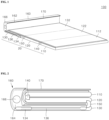
- FIG. 1 is a perspective view schematically showing an external shape of a display device according to an example embodiment of the present disclosure
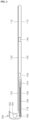
- FIG. 2 is a side view showing an example in which a display face is protected by a transparent cover when a display device according to an example embodiment of the present disclosure is folded.
- FIG. 3 is a side view of a display device according to an example embodiment of the present disclosure while unfolded.
- FIG. 4 is a side view showing an example in which a transparent cover is slid into a cover-receiving hole when a display device according to an example embodiment of the present disclosure is folded
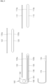
- FIG. 5 shows cross-sectional views viewed from the side of disassembled first to third panel areas according to an example embodiment of the present disclosure.
- a display device 100 includes a display panel 20 having a first panel area 110, a second panel area 120, and a third panel area 130.
- the first panel area 110 includes a first front face 110a and a first rear face 110b.
- the first front face 110a may have the same area as or may have a smaller area than the first rear face 110b.
- the first panel area 110 may include a first display unit 112 on the first front face 110a.
- the first display unit 112 may have the same area as or may have a smaller area than the first front face 110a.
- the second panel area 120 includes a second front face 120a and a second rear face 120b.
- the second front face 120a may have the same area as or may have a smaller area than the second rear face 120b.
- the second panel area 120 may include a second display unit 122 on the second front face 120a.
- the second display unit 122 may have the same area as or a smaller area than the second front face 120a.
- the third panel area 130 includes a third front face 130a and a third rear face 130b.
- the third front face 130a may have the same area as or a smaller area than the third rear face 130b.
- the third panel area 130 may include a third display unit 132 on the third front face 130a.
- the third display unit 132 may have the same area as or a smaller area than the third front face 130a.
- each of the first panel area 110, the second panel area 120, and the third panel area 130 may include an active area (AA) that is configured to displays an image, and a non-active area (NA) that is configured to supply one or more signals to the active area.
- AA active area
- NA non-active area
- the first panel area 110 may include the first display unit 112.
- the first panel area 110 may have the same area as the first display unit 112 or may have a larger area than the first display unit 112.
- the second panel area 120 may include the second display unit 122.
- the second panel area 120 may have the same area as the second display unit 122 or may have a larger area than the second display unit 122.
- the third panel area 130 may include the third display unit 132.
- the third panel area 130 may have the same area as the third display unit 132 or may have a larger area than the third display unit 132.
- first panel area 110, the second panel area 120, and the third panel area 130 have the same size and area as described above, internal structures thereof may be identical or similar. Accordingly, a description will be made using the third panel area 130 as an example for example embodiments in which the first panel area 110, the second panel area 120, and the third panel area 130 have the same structure. However, the present disclosure is not limited thereto.
- the third panel area 130 may include a substrate therein, and a light blocking layer and a buffer layer may be disposed on the substrate. That is, the light blocking layer may be disposed on the substrate, and the buffer layer may be disposed on the light blocking layer.
- the substrate may be formed with polymethylmethacrylate (PMMA), vinyl chloride, an acrylic resin, a polycarbonate (PC)-based resin, a polyethylene terephthalate (PET)-based resin, a polyethylene (PE)-based resin, a polystyrene (PS)-based resin, a polypropylene (PP)-based resin, a polyimide (PI)-based resin, a glass, a silica, and the like.
- PMMA polymethylmethacrylate
- PC polycarbonate
- PET polyethylene terephthalate
- PS polystyrene
- PP polypropylene
- PI polyimide
- the light blocking layer may be made of a metal material having a light blocking function in order to block an inflow of external light.
- the light blocking layer may be formed in a single-layer or multi-layer structure made of one of metals such as molybdenum (Mo), aluminum (Al), chromium (Cr), tungsten (W), titanium (Ti), nickel (Ni), neodymium (Nd), and copper (Cu) or an alloy thereof.
- the buffer layer may be formed on the substrate and on the light blocking layer.
- the buffer layer covering the light blocking layer on the substrate may be formed in a structure in which a single insulating layer or a plurality of insulating layers are stacked in order to block foreign materials including moisture, oxygen, and the like from being introduced from the substrate.
- the buffer layer may be formed in a single-layer or multi-layer structure of an inorganic insulating material such as a silicon oxide (SiOx), a silicon nitride (SiNx), or an aluminum oxide (AlOx).
- the third panel area 130 may have the third display unit 132 disposed on the uppermost layer.
- the third display unit 130 includes a plurality of scan lines respectively disposed in rows, a plurality of data lines respectively disposed in columns and intersecting the scan lines, and a plurality of pixels respectively disposed at intersections between the scan lines and the data lines.
- Each pixel may include at least one sub-pixel. Accordingly, the sub-pixels may be disposed at each intersection.
- the plurality of scan lines and the plurality of data lines intersect each other on the glass substrate or the plastic substrate.
- Sub-pixels respectively having colors of red, green, and blue may be defined at each point where the scan line and a data line intersect each other.
- One pixel including at least one sub-pixel may be referred to as a "unit pixel”.
- each of the sub-pixels may include an organic light emitting diode (OLED).
- OLED organic light emitting diode
- the plurality of scan lines may be respectively disposed in rows of the plurality of sub-pixels, and the plurality of data lines may be respectively disposed in columns of the plurality of sub-pixels. Accordingly, in the plurality of sub-pixels, the light emitting diodes (OLEDs) may be arranged in rows and columns.
- the organic light emitting diode may be simply referred to as the "light emitting diode (OLED)", a “light emitting diode (EL)”, a “light emitting device (EL)", the “EL” or the “OLED”.
- a power line formed in a direction parallel to the data line may be formed to be connected to the sub-pixels.
- each sub-pixel may include at least one organic light emitting diode, a capacitor, a switching thin film transistor, and a driving thin-film transistor.
- the driving thin-film transistor may be referred to as a “driving transistor”, a “driving switch”, a “driving device”, and the like.
- each organic light emitting diodes may emit light with an amount of current adjusted based on a voltage between the gate and the source electrodes of the driving thin-film transistor.
- An anode of the organic light emitting diode (OLED) may be connected to a high-potential voltage power supply, and a cathode may be connected to a low-potential voltage power supply.
- An organic compound layer may be disposed between the anode and the cathode.
- the organic compound layer may include a hole injection layer (HIL), a hole transport layer (HTL), an emission layer (EML), an electron transport layer (ETL), and an electron injection layer (EIL), but the present disclosure may not be limited thereto.
- HIL hole injection layer
- HTL hole transport layer
- EML emission layer
- ETL electron transport layer
- EIL electron injection layer
- at least two organic compound layers emitting light of different colors may be stacked based on a tandem structure.
- OLED organic light emitting diode
- holes that have passed through the hole transport layer (HTL) and electrons that have passed through the electron transport layer (ETL) may move to the emission layer (EML) to form excitons.
- EML electron injection layer
- the driving thin-film transistor and the switching thin film transistors may be connected to a gate line (herein also referred to as scan line), a control signal supply line, and a data line. Accordingly, the current may flow through the switching thin-film transistors based on a gate voltage input to the gate line (scan line), and at the same time, the switching thin-film transistors may transfer a data voltage input to the data line to the driving thin-film transistor.
- the capacitor may be interposed between and connected to the thin film transistor and the power line, may be charged with the data voltage transmitted from the thin film transistor, and may keeps the charges for 1 frame.
- the thin film transistor may be implemented as a PMOS-type low temperature poly silicon (LTPS) TFT, thereby ensuring desired response characteristics.
- LTPS low temperature poly silicon
- at least one transistor may be implemented as an NMOS-type or PMOS-type oxide TFT having good leakage current characteristics when being turned-off, and the remaining transistors may be implemented as the PMOS-type LTPS TFT having the good response characteristics.
- the first panel area 110 may include the first display unit 112, the second panel area 120 may include the second display unit 122, and the third panel area 130 may include the third display unit 132.
- the first display unit 112, the second display unit 122, and the third display unit 132 may all have the same structure. Detailed structures of the first display unit 112, the second display unit 122, and the third display unit 132 will be described later.
- the second rear face 120b of the second panel area 120 faces the first rear face 110b of the first panel area 110 and corresponds to the first panel area 110.
- a first hinge coupling portion 140 hinge-couples one end of the first panel area 110 and one end of the second panel area 120 to each other.
- a left end of the first panel area 110 may be hinge-coupled to a right end of the second panel area 120 through the first hinge coupling portion 140.
- the third front face 130a of the third panel area(130) faces the second front face 120a of the second panel area 120 and corresponds to the second panel area 120.
- a second hinge coupling portion 150 hinge-couples another end of the second panel area 120, which is opposite to the one end of the second panel area 120, and one end of the third panel area 130 to each other. For example, as shown in FIG. 1 , a left end of the second panel area 120 may be hinge-coupled to a right end of the third panel area 130 through the second hinge coupling portion 150.
- Another end of the third panel area 130 which is opposite to the one end of the third panel area 130, extends with the same width as a vertical width to form an outer body 160 or may be coupled to the outer body 160.
- a left end of the third panel area 130 may extend with the same width as a width(that is, a dimension a direction along which the boundary between the second and third panel areas 120 and 130 extends, hereinafter referred to as "boundary extending direction") of the third panel area 130 to form an outer body 160 or may be coupled to the outer body 160.
- the outer body 160 may be formed to extend from the left end of the third panel area 130 with the same width as the width of the third panel area 130.
- the outer body 160 may have a thickness (that is, a dimension in a direction in perpendicular to the boundary extending direction) and a vertical dimension (that is, a dimension in a direction in perpendicular to a display plane of the third display unit 132), each being greater than a thickness (that is, a dimension in a direction in perpendicular to a display plane of the third display unit 132) of the third panel area 130.
- the first panel area 110, the second panel area 120, and the third panel area 130 are continously arranged and are integrally formed with each other. That is, the first display unit 112 of the first panel area 110, the second display unit 122 of the second panel area 120, and the third display unit 132 of the third panel area 130 may all be continuously arranged and may be integrally formed with each other.
- the first display unit 112 as the first front face 110a of the first panel area 110, the second display unit 122 as the second front face 120a of the second panel area 120, and the third display unit 132 as the third front face 130a of the third panel area 130 may all be continuously arranged and may be integrally formed with each other.
- the first hinge coupling portion 140 is disposed between the first panel area 110 and the second panel area 120. Accordingly, the first panel area 110 and the second panel area 120 may be folded or unfolded by a hinge operation.
- a boundary between the first display unit 112 and the second display unit 122 may be bent and folded or unfolded.
- the second hinge coupling portion 150 is disposed between the second panel area 120 and the third panel area 130. Accordingly, the second panel area 120 and the third panel area 130 may be folded or unfolded by the hinge operation.
- a boundary between the second display unit 122 and the third display unit 132 may be bent and folded or unfolded.
- the first panel area 110, the second panel area 120, and the third panel area 130 When the first panel area 110, the second panel area 120, and the third panel area 130 are unfolded, because the first display unit 112, the second display unit 122, and the third display unit 132 are all continuously arranged and are integrally formed with each other, the first panel area 110, the second panel area 120, and the third panel area 130 may operate as one display screen.
- an image to be displayed on one display screen may be divided into three screen images, so that a first screen image may be displayed on the first display unit 112, a second screen image may be displayed on the second display unit 122, and a third screen image may be displayed on the third display unit 132.
- the outer body 160 has the greater thickness and vertical dimension than the thickness of the third panel area 130, when the first panel area 110, the second panel area 120, and the third panel area 130 are unfolded, the outer body 160 may serve as a handle.
- the outer body 160 When the first panel area 110, the second panel area 120, and the third panel area 130 are in the folded state, the outer body 160 has a shape formed so as to surround and face the one end of the first panel area 110, the one end of the second panel area 120, and the first hinge coupling portion 140.
- a cover-receiving hole 162 into which a transparent cover 170 is inserted is formed in the outer body 160, and an accommodation space 164 for accommodating therein the transparent cover 170 inserted into the cover-receiving hole 162 is formed inside the outer body 160.
- the third panel area 130 is positioned as the lowermost panel area, the second panel area 120 is located on the third panel area 130, and the first panel area 110 may be located on the second panel area 120.
- the first panel area 110 When the first panel area 110, the second panel area 120, and the third panel area 130 are in the folded state, the first panel area 110 is positioned as the uppermost panel area, and the transparent cover 170 may be located on the first panel area 110.
- the transparent cover 170 may be positioned to cover the first front face 110a of the first panel area 110. That is, the transparent cover 170 may protrude from the cover-receiving hole 162 of the outer body 160 and be positioned to cover the first display unit 112 disposed on the first panel area 110.
- a moving holder 134 connected to the transparent cover 170 may be disposed at a lower end of the third panel area 130 integrally formed with the outer body 160 so as to move the transparent cover 170.
- a moving rail 136 that provides a movement path of the moving holder 134 may be defined.
- the moving rail 136 may be defined as long as a movement distance of the transparent cover 170 in a form of a groove into which a portion of the moving holder 134 is inserted. That is, as the moving holder 134 and the transparent cover 170 are connected to each other, the transparent cover 170 may protrude from or be inserted into the cover-receiving hole 162 of the outer body 160 as much as the movement distance of the moving holder 134.
- the transparent cover 170 When the moving holder 134 moves from one side to the other side along the moving rail 136, the transparent cover 170 may be inserted into the cover-receiving hole 162 to be located in the accommodation space 164. For example, when the moving holder 134 moves from a left end to a right end along the moving rail 136 as shown in FIG. 4 , the transparent cover 170 may be inserted into the cover-receiving hole 162 of the outer body 160 and may be located in the accommodation space 164.
- the transparent cover 170 may protrude outwardly from the cover-receiving hole 162 so as to cover the third front face 130a of the third panel area 130(in the unfolded state).
- the transparent cover 170 connected to the moving holder 134 may outwardly protrudes from the cover-receiving hole 162 of the outer body 160 and be positioned so as to cover the first display unit 112 of the first panel area 110.
- the outer body 160 may include a storage hole 166 for storing a touch pen inserted thereinto. That is, the outer body 160 may include the storage hole 166 having a length equal to or greater than a length of the touch pen in the accommodation space 164 therein. Accordingly, a user may easily perform a touch input on the screen of the first display unit 112 in the folded state or on the screen formed by the first, second, and third display units 112, 122 and 132 in the unfolded state using the touch pen disposed in the storage hole 166 of the outer body 160.
- FIG. 6 is a schematic diagram showing a front face of a display device according to an example embodiment of the present disclosure when folded
- FIG. 7 is a schematic diagram showing a rear face of a display device according to an example embodiment of the present disclosure when folded.
- the outer body 160 may include a camera 180, a speaker 182, a flash unit 184, and an illuminometer 186.
- the camera 180 may be for obtaining an image by photographing an external object.
- a lens may be positioned so as to be viewed via a through-hole of the outer body 160, and an internal circuit may be disposed in the accommodation space 164 of the outer body 160.
- the speaker 182 may be for outputting sound.
- the speaker 182 may include a cover-receiving hole for inserting a separate earphone jack therein.
- the flash unit 184 may be for light output.
- the flash unit 184 may be driven, for example, during operation of the camera 180 at night.
- the illuminometer 186 may be for detecting ambient brightness.
- the illuminometer 186 may detect the ambient brightness through an illuminance sensor, so that the illuminometer 186 may be used to automatically operate the flash unit 184 when the camera 180 is operated at night.
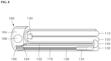
- FIG. 8 is a schematic diagram showing an electrical connection relationship between a third panel area and an outer body in a display device according to an example embodiment of the present disclosure
- FIG. 9 is a schematic diagram showing a contact state between a third panel area and a printed circuit board of an outer body of a display device according to an example embodiment of the present disclosure.
- the outer body 160 of the display device 100 may include a printed circuit board (PCB) 190 in the accommodation space 164.
- PCB printed circuit board
- the printed circuit board 190 may be disposed inside the outer body 160, and may be electrically connected to the camera 180, the speaker 182, the flash unit 184, and the illuminometer 186.
- the printed circuit board 190 may be electrically connected to the third display unit 132 of the third panel area 130 through one or more flexible printed circuit boards (FPCB) 194.
- FPCB flexible printed circuit boards
- the printed circuit board (PCB) 190 may have at least one contact hole 192 formed therein.
- the printed circuit board (PCB) 190 may be electrically connected to the flexible printed circuit board (FPCB) 194 via the at least one contact hole 192.
- the flexible printed circuit board (FPCB) 194 may connect the printed circuit board (PCB) 190 and the third panel area 130 to each other or electrically connect the printed circuit board (PCB) 190 and the third display unit 132 of the third panel area 130 to each other.
- the flexible printed circuit board 194 may have one side electrically in contact with the third display unit 132 of the third panel area 130, and the other side electrically in contact with the printed circuit board (PCB) 190 via the at least one contact hole 192.
- the printed circuit board (PCB) 190 may have a through-hole defined therein in which the camera 180 extends.
- a through-hole through which the camera 180 is visually recognized may also be defined in an outer face of the outer body 160. Therefore, the camera 180 may be located in the accommodation space 164 inside the outer body 160, may extend through the printed circuit board (PCB) 190 via the through-hole, and may be visually recognized from the outside via the through-hole of the outer face of the outer body 160.
- FIG. 10 is a diagram showing an example of displaying an image when a display device according to an example embodiment of the present disclosure is in a folded state
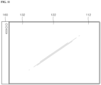
- FIG. 11 is a diagram showing an example of displaying an image when a display device according to an example embodiment of the present disclosure is in an unfolded state.
- the first panel area 110 is located at the top.
- the display device 100 may have the outer body 160 positioned on the left end thereof, and the first panel area 110 positioned on the right end.
- the first panel area 110 may display the image through the first display unit 112.
- the image displayed on the first display unit 112 may be one image having an area corresponding to an area of the first display unit 112 based on a lateral dimension (that is, a dimension in the boundary extending direction) and a longitudinal dimension (that is, a dimension in a direction in perpendicular to the boundary extending direction). That is, said one image may be the one screen image that is not divided into the three screen images.
- the first display unit 112 when the first panel area 110, the second panel area 120, and the third panel area 130 are in the unfolded state, the first display unit 112, the second display unit 122, and the third display unit 132 may form one display screen that is continuously and integrally formed.
- said one display screen may be a screen having an area that is a sum of a first area based on lateral and longitudinal dimensions of the first display unit 112, a second area based on lateral and longitudinal dimensions of the second display unit 122, and a third area based on lateral and longitudinal dimensions of the third display unit 132.
- the images displayed through the first display unit 112, the second display unit 122, and the third display unit 132 may be divided images divided into a first image corresponding to the first area, a second image corresponding to the second area, and a third image corresponding to the third area, respectively.
- the display device 100 may display said one image as the first image is output from the first display unit 112, the second image is output from the second display unit 122, and the third image is output from the third display unit 132.
- FIG. 12 is a block diagram schematically showing a configuration of a third panel area in a display device according to an example embodiment of the present disclosure
- FIG. 13 is a block diagram schematically showing an example pixel configuration.
- the third panel area 130 may include an active area AA and a non-active area NA other than the active area.
- first panel area 110 and the second panel area 120 also have the same structure as the third panel area 130, and components of the third panel area 130 described below may be equally applicable to the first panel area 110 and the second panel area 120.
- the active area AA may include the third display unit 132 including a plurality of sub-pixels (PXs) arranged in rows and columns. Therefore, an active area of the first panel area 110 may include the first display unit 112, and an active area of the second panel area 120 may include the second display unit 122.
- PXs sub-pixels
- each sub-pixel PX may be defined at a corresponding intersection therebetween.
- each sub-pixel PX may include the organic light emitting diode (OLED).
- the third display unit 132 may include a glass substrate or a plastic substrate, the plurality of scan lines Scan #1 to Scan #n and the plurality of data lines D1_1, D1_2 to Dn_1, Dn_2 disposed on the glass substrate or the plastic substrate, and intersecting each other, and sub-pixels R, G, and B corresponding to red, green, and blue, respectively, and respectively defined at the intersections between the scan lines Scan #1 to Scan #n and the data lines D1_1, D1_2 to Dn_1, Dn_2.
- the plurality of scan lines Scan #1 to Scan #n may be arranged such that one scan line is disposed in each of rows composed of the plurality of sub-pixels, as shown in FIG. 13 .
- the plurality of data lines D1_1, D1_2 to Dn_1, and Dn_2 may be arranged such that two data lines are disposed in each of columns composed of the plurality of sub-pixels, as shown in FIG. 13 .
- Each of the scan lines may be connected to a scan driver 30 and each of the data lines to a data driver 40.
- power supply voltage supply lines ELVDD, Vini, and ELVSS may be further formed in a direction parallel to the data lines D1_1, D1_2 to Dn_1, and Dn_2 and be connected to each sub-pixel.
- a given pixel may include at least one of a first sub-pixel (for example, red sub-pixel R1, R2), a second sub-pixel (for example, green sub-pixel G1, G2) and a third sub-pixel (for example, blue sub-pixel B1, B2) as shown in FIG. 13 .
- One pixel may include two second sub-pixel G1 and G2, as show in FIG. 13 .
- one scan line Scan #1 may be disposed in each row, and two data lines may be disposed in each column.
- a data line D1_1 may be disposed at one side (Left) of the column
- a data line D1_2 may be disposed at the other side (Right) of the column. That is, in one sub-pixel R1, one scan line Scan #1 and two data lines D1_1 and D1_2 may be disposed.
- the third display unit 132 may include a first multiplexer MUX 1 that is configured to selects the data line D1_1 of one side (Left) among the two data lines disposed in each column, and a second multiplexer MUX 2 that is configured to selects the data line D1_2 of the other side (Right) among the two data lines disposed in each column.
- the third display unit 132 may include a first scan switch T-Sc1 for switching the scan line Scan #1 disposed in a first row to be connected to the data line D1_1 of one side (Left) disposed in each column, a second scan switch T-Sc2 for switching the scan line Scan #2 disposed in a second row to be connected to the data line D1_1 of one side (Left) disposed in each column, a third scan switch T-Sc3 for switching the scan line Scan #3 disposed in a third row to be connected to the data line D1_2 of the other side (Right) disposed in each column, and a fourth scan switch T-Sc4 for switching the scan line Scan #4 disposed in a fourth row to be connected to the data line D1_2 of the other side (Right) disposed in each column.
- each of the first scan switch T-Sc1 to the fourth scan switch T-Sc4 may be implemented as, for example, a thin-film transistor (TFT).
- the first and second scan switches T-Sc1 and T-Sc2 may be respectively disposed in two sub-pixels consecutively arranged in a column direction along the data line D1_1 at one side (Left) among a plurality of sub-pixels, for example, a first red sub-pixel R1 and a first blue sub-pixel B 1.
- the two sub-pixels consecutively arranged in the column direction along the data line D1_1 of one side (Left) may be sub-pixels R1 and B1 of different colors, or sub-pixels G3 and G4 of the same color.
- the third and fourth scan switches T-Sc3 and T-Sc4 may be respectively disposed in two sub-pixels consecutively arranged in the column direction along the data line D1_2 of the other side (Right) among the plurality of sub-pixels, for example, a second red sub-pixel R2 and a second blue sub-pixel B2.
- the two sub-pixels consecutively arranged in the column direction along the data line D1_2 of the other side (Right) may be sub-pixels R2 and B2 of different colors, or sub-pixels G1 and G2 of the same color.
- the first and second scan switches T-Sc1 and T-Sc2 and the third and fourth scan switches T-Sc3 and T-Sc4 may be arranged along the plurality of sub-pixels arranged in the column direction such that the first and second scan switches T-Sc1 and T-Sc2 may be disposed at a left side and the third and fourth scan switches T-Sc3 and T-Sc4 may be disposed at a right side.
- the first multiplexer MUX 1 in FIG. 13 may include a first multiplexer switch T-MX1 having a first electrode connected to the data line D1_1 of one side (Left), a gate electrode connected to a first multiplexer line MUX1 for applying a first selection signal, and a second electrode connected to first power ELVDD.
- the first multiplexer switch T-MX1 in FIG. 13 may be turned on as the first selection signal is applied to the gate electrode through the first multiplexer line MUX1.
- the first power ELVDD applied through the second electrode of the first multiplexer switch T-MX1 may be applied to the data line D1_1 of one side (Left) through the first electrode.
- the second multiplexer MUX 2 in FIG. 13 may include a second multiplexer switch T-MX2 having a first electrode connected to the data line D1_2 of the other side (Right), a gate electrode connected to a second multiplexer line MUX2 for applying a second selection signal, and a second electrode connected to the first power ELVDD.
- the second multiplexer switch T-MX2 in FIG. 13 may be turned on as the second selection signal is applied to the gate electrode through the second multiplexer line MUX2.
- the first power ELVDD applied through the second electrode may be applied to the data line D1_2 of the other side (Right) through the first electrode.
- each sub-pixel may include at least one organic electroluminescent diode OLED, a capacitor Cst, switching thin-film transistors T1 and T2 and a driving thin-film transistor Tdr.
- the organic electroluminescent diode OLED may include a first electrode (hole injection electrode), an organic compound layer, and a second electrode (electron injection electrode).
- the organic compound layer may include a light-emitting layer for emitting light and may further include various organic layers for efficiently transferring carriers including holes or electrons to the light-emitting layer. These organic layers may include a hole injection layer and a hole transport layer positioned between the first electrode and the light-emitting layer, and an electron injection layer and an electron transport layer positioned between the second electrode and the light-emitting layer.
- the non-active area NA may be located inside the rear face of the third display unit 132, and may include a luminance controller 10, the scan driver 30, the data driver 40, a light-emission controller 50, a power supply 60, and a timing controller 70.
- the luminance controller 10 may provide one gamma set selected from among a plurality of gamma sets each including a plurality of gamma data to the data driver 40, and provide dimming data corresponding to the selected gamma set to the light-emission controller 50.
- the scan driver 30 may apply a scan signal to the plurality of scan lines Scan #1 to Scan #n. For example, the scan driver 30 may sequentially apply a gate voltage to the sub-pixels on one horizontal line basis in response to a gate control signal GCS input thereto.
- the scan driver 30 may be implemented as a shift register having multiple stages that sequentially output a high-level gate voltage every one horizontal period H.
- the data driver 40 may apply a data signal to the plurality of data lines D1_1, D1_2 to Dn_1, and Dn_2.
- the data driver 40 receives an image signal of a digital waveform applied from the timing controller 70, converts the image signal into a data voltage as an analog voltage having a gray level value that each sub-pixel may process, and then supplies the data voltage to each sub-pixel through the data lines D1_1, D1_2 to Dn_1, Dn_2 in response to a data control signal DCS input thereto.
- the data driver 40 may convert the image signal into the data voltage based on multiple reference voltages supplied from a reference voltage supplier (not shown).
- the data driver 40 may apply low-potential voltage ELVSS and initialization voltage Vini in a 30 Hz operation mode and low-potential voltage ELVSS and initialization voltage Vini in a 60 Hz operation mode to the third display unit 132 such that the low-potential voltage ELVSS and initialization voltage Vini in a 30 Hz operation mode are different from low-potential voltage ELVSS and initialization voltage Vini in a 60 Hz operation mode.
- the data driver 40 may provide the low-potential voltage ELVSS and the initialization voltage Vini having the same value to the third display unit 132 in the 30 Hz operation mode.
- the data driver 40 may provide the third display unit 132 with the low-potential voltage ELVSS and the initialization voltage Vini different from the low-potential voltage ELVSS and the initialization voltage Vini in the 30 Hz operation mode.
- the data driver 40 may provide the third display unit 132 with the low-potential voltage ELVSS and the initialization voltage Vini such that a difference between the low-potential voltage ELVSS and the initialization voltage Vini is greater than or equal to a predefined reference.
- the data driver 40 may provide the low-potential voltage ELVSS and the initialization voltage Vini corresponding to said one selected gamma set based on a look-up table to the third display unit 132.
- the light-emission controller 50 may apply light-emission control signals EM 1 to EM n to the plurality of sub-pixels.
- the power supply 60 may provide high-potential voltage ELVDD, low-potential voltage ELVSS, and initialization voltage Vini to each sub-pixel.
- the timing controller 70 may control the scan driver 30 and the data driver 40.
- the timing controller 70 may receive an image signal, a clock signal, and timing signals such as vertical and horizontal synchronization signals from an external system, may generate the gate control signal GCS and the data control signal DCS, based on the received signals, and may provide the gate control signal GCS and the data control signal DCS respectively to the scan driver 30 and the data driver 40.
- the horizontal synchronization signal indicates a time it takes to display one line of a display screen
- the vertical synchronization signal may indicate a time it takes to display a display screen of one frame.
- the clock signal may refers to a signal based on which control signals of and each of the drivers (e.g., the scan driver 30 and the data driver 40) are generated based.
- the timing controller 70 may be connected to an external system through a predetermined interface and may receive an image-related signal and a timing signal output therefrom at high speed without noise.
- the interface may include a LVDS (Low Voltage Differential Signal) scheme interface or a TTL (Transistor-Transistor Logic) scheme interface.
- FIG. 14 is a circuit diagram showing an example circuit configuration of one sub-pixel in a third panel area according to an example embodiment of the present disclosure.
- one sub-pixel may include a plurality of thin-film transistors T1 to T6, an organic electroluminescent diode OLED, a driving thin-film transistor Tdr, and an internal compensation circuit.
- the organic electroluminescent diode may be simply referred to as 'light-emitting diode (OLED)', 'light-emitting diode (EL)', 'light-emitting element (EL)', 'EL' or 'OLED'.
- the driving thin-film transistor Tdr may be referred to as ⁇ driving transistor Tdr' or ⁇ driving switch Tdr'.
- At least one (e.g., all) of the thin-film transistors T1 to T6 and Tdr included in the sub-pixel may be implemented as PMOS-type LTPS (Low Temperature Poly Silicon) TFT.
- PMOS-type LTPS Low Temperature Poly Silicon
- desired response characteristics may be secured.
- at least one transistor among the thin-film transistors T1 to T6 may be implemented as an NMOS type or PMOS type oxide TFT with good leakage current characteristics when being turned off, while each of the remaining transistors may be implemented as a PMOS type LTPS TFT with good response characteristics.
- the present disclosure is not limited thereto.
- the OLED may emits light based on an amount of current adjusted based on a gate-source voltage Vgs of the driving thin-film transistor Tdr.
- An anode electrode of the OLED may be connected to a node P8, and a cathode electrode of the OLED may be connected to low-potential power voltage ELVSS.
- An organic compound layer may be formed between the anode electrode and the cathode electrode.
- the organic compound layer may include a hole injection layer (HIL), a hole transport layer (HTL), an emission layer (EML), an electron transport layer (ETL), and an electron injection layer (EIL).
- HIL hole injection layer
- HTL hole transport layer
- EML emission layer
- ETL electron transport layer
- EIL electron injection layer
- the present disclosure is not limited thereto.
- two or more organic compound layers emitting different colors may be stacked according to a tandem structure.
- a current flows through the light-emitting diode (OLED) holes passing through the hole transport layer (HTL) and electrons passing through the electron transport layer (ETL) may move to the light-emitting layer (EML) and may be combined with each other therein to form excitons.
- the light-emitting layer (EML) may emits visible light.
- the driving thin-film transistor Tdr is a driving element that may control current flowing through the (OLED) based on the gate-source voltage Vgs thereof.
- the driving thin-film transistor Tdr may have a gate electrode connected to a node P5, one of first and second electrodes connected to a node P2 and the other thereof connected to a node P6.
- the gate-source voltage Vgs of the driving transistor Tdr may refers to a voltage across the node P5 and the node P6.
- the first thin-film transistor T1 operating based on an n-th first scan signal S1(n) may be connected to and disposed between the node P5 and the node P6. That is, the first thin-film transistor T1 may be configured to have one of its first and second electrodes connected to the node P5, the other connected to the node P6, and its gate electrode connected, for example, through a node P7, to a line for receiving the n-th first scan signal S1(n).
- the second thin-film transistor T2 connected to a data line Vdata may be connected to the node P2. That is, the second thin-film transistor T2 may be configured to have one of its first and second electrodes connected to the data line Vdata (at P1), the other connected to the node P2, and its gate electrode connected to a line for receiving the n-th first scan signal S1(n)(at P7).
- the first thin-film transistor T1 and the second thin-film transistor T2 may be turned on based on the n-th first scan signal S1(n).
- the gate electrode of the driving transistor Tdr may be connected to a first electrode of the storage capacitor Cst.
- a second electrode of the storage capacitor Cst may be connected to first power, that is, high-potential power VDD(e.g., ELVDD).
- the third thin-film transistor T3 may be connected to and disposed between the first electrode of the driving transistor Tdr and the second electrode of the storage capacitor Cst. That is, the third thin-film transistor T3 may be configured to have one of its first electrode and second electrode connected to the node P2, the other connected to the node P3, and its gate electrode connected to a line for receiving a light-emission control signal EM.
- the fourth thin-film transistor T4 may be connected to and disposed between the second electrode the driving transistor Tdr and the anode electrode the OLED. That is, the fourth thin-film transistor T4 may be configured such that one of its first electrode and second electrode is connected to the node P6, the other is connected to the node P8, and its gate electrode is connected to a line for receiving the light-emission control signal EM.
- the third thin-film transistor T3 and the fourth thin-film transistor T4 may be turned on based on the light-emission control signal EM.
- the fifth thin-film transistor T5 may be connected to the first electrode of the storage capacitor Cst. That is, the fifth thin-film transistor T5 may be configured such that one of its first and second electrodes is connected to the node P4, the other is connected to a first initialization voltage line Vinit1, and its gate electrode is connected, for example, through a node P9, to a line to which an (n-4)-th second scan signal S2(n-4) is applied.
- the sixth thin-film transistor T6 may be connected to the anode electrode of the OLED. That is, the sixth thin-film transistor T6 may be configured such that one of its first and second electrodes is connected to the node P8, the other thereof is connected to a second initialization voltage line Vinit2, and its gate electrode thereof is connected to a line to which the (n-4)-th second scan signal S2(n-4) is applied.
- the compensation circuit may be configured for sampling the gate-source voltage Vgs in order to compensate for change in a threshold voltage of the driving transistor Tdr, and may be configured to include the first to sixth thin-film transistors T1 to T6 and the storage capacitor Cst.
- the driving transistor Tdr may control current flowing through the light-emitting diode OLED based on the data signal Vdata. In this regard, luminance of the OLED may be adjusted based on a magnitude of the current.
- the third and fourth thin-film transistors T3 and T4 as light-emission control transistors may be connected to the driving transistor Tdr and the light-emitting diode OLED to control light emission of the OLED.
- the third and fourth thin-film transistors T3 and T4 as the light-emission control transistors may be turned on, such that the current flowing through the driving transistor Tdr may be transmitted to the OLED so that the OLED may emit light.
- the third and fourth thin-film transistors T3 and T4 are turned off, the current flowing through the driving transistor Tdr may be not transmitted to the OLED, and thus the OLED may not emit light.
- luminance of the display device may be determined based on a magnitude of current supplied from the driving transistor Tdr and a time duration for which the light-emission control transistors T3 and T4 are turned on.
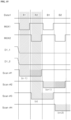
- FIG. 15 is a diagram showing an interlace scheme operation timing diagram of a third panel area according to an example embodiment of the present disclosure.
- the third panel area 130 may operate in an interlaced scheme.
- one frame may be divided into a first half frame and a second half frame.
- sub-pixels R1 and R2 disposed in an odd-numbered row may operate.
- sub-pixels B1 and B2 disposed in an even-numbered row operate.
- the third panel area 130 may activates an odd-numbered rows for the first half frame of a single frame, and may activate an even-numbered rows for the second half frame of the single frame.
- the first multiplexer MUX1 (e.g., the first multiplexer switch T-MX1) may be turned on based on a low signal
- the second multiplexer MUX2 (e.g., the second multiplexer switch T-MX2) may be turned off based on a high signal.
- a low signal may be applied to both the data line D1_1 of one side (Left) and the data line D1_2 of the other side (Right).
- an (n-1)-th first scan signal as a low signal may be applied to a first scan line Scan #1 for two horizontal periods (2H).
- the first scan switch T-Sc1 may be turned on, and thus, a low signal from the data line D1_1 of one side (Left) may be applied to a first red sub-pixel R1 disposed in an odd-numbered first row. Accordingly, the first red sub-pixel R1 disposed in the odd-numbered first row may operates to emit light.
- the first multiplexer MUX1 (e.g., the first multiplexer switch T-MX1) may be turned off based on a high signal
- the second multiplexer MUX2 (e.g., the second multiplexer switch T-MX2) may be turned on based on a low signal.
- a low signal may be applied to both the data line D1_1 of one side (Left) and the data line D1_2 of the other side (Right).
- an n-th third scan signal as a low signal is applied to a third scan line Scan #3 for two horizontal periods (2H).
- the third scan switch T-Sc3 may be turned on, and thus, a low signal from the data line D1_2 of the other side (Right) is applied to a second red sub-pixel R2 disposed in an odd-numbered third row. Accordingly, the second red sub-pixel R2 disposed in the odd-numbered third row may operate to emit light.
- the (n-1)-th first scan signal applied to the first scan line Scan #1 has a low level for first two horizontal periods (2H).
- the n-th third scan signal applied to the third scan line Scan #3 may be at a low level state for two horizontal periods (2H). That is, when an operation of the first red sub-pixel R1 is switched to an operation of the second red sub-pixel R2, a low level of the (n-1)-th first scan signal applied to the first scan line Scan #1 and a low level of the n-th third scan signal applied to the third scan line Scan #3 overlap each other for one horizontal period (1H). Therefore, when an operation of the first red sub-pixel R1 is switched to an operation of the second red sub-pixel R2, flicker phenomenon may not occur.
- the first multiplexer MUX1 (e.g., the first multiplexer switch T-MX1) may be turned on based on a low signal
- the second multiplexer MUX2 (e.g., the second multiplexer switch T-MX2) may be turned off based on a high signal.
- a low signal may be applied to both the data line D1_1 of one side (Left) and the data line D1_2 of the other side (Right).
- a (n+1)-th second scan signal as a low signal may be applied to the second scan line Scan #2 for two horizontal periods (2H).
- the second scan switch T-Sc2 is turned on, and thus, a low signal from the data line D1_1 of one side (Left) may be applied to a first blue sub-pixel B1 disposed in an even-numbered second row. Accordingly, the first blue sub-pixel B1 disposed in the even-numbered second row may operate to emit light.
- the first multiplexer MUX1 (e.g., the first multiplexer switch T-MX1) may be turned off based on a high signal
- the second multiplexer MUX2 (e.g., the second multiplexer switch T-MX2) may be turned on based on a low signal.
- a low signal may be applied to both the data line D1_1 of one side (Left) and the data line D1_2 of the other side (Right).
- an (n+2)-th fourth scan signal as a low signal may be applied to the fourth scan line Scan #4 for two horizontal periods (2H).
- the fourth scan switch T-Sc4 may be turned on, and thus, a low signal from the data line D1_2 of the other side (Right) may be applied to a second blue sub-pixel B2 disposed in an even-numbered fourth row. Accordingly, the second blue sub-pixel B2 disposed in the even-numbered fourth row may operate to emit light.
- the (n+1)-th second scan signal applied to the second scan line Scan #2 may be at a low level state for two horizontal periods (2H).
- the (n+2)-th fourth scan signal applied to the fourth scan line Scan #4 may be at a low level state for two horizontal periods (2H). That is, when an operation of the first blue sub-pixel B1 is switched to an operation of the second blue sub-pixel B2, a low level of the (n+1)-th second scan signal applied to the second scan line Scan #2 and a low level of the (n+2)-th fourth scan signal applied to the fourth scan line Scan #4 may overlap each other for one horizontal period (1H).
- the flicker when the third panel area 130 operates in the interlace scheme, the flicker may not occur when an operation of one sub-pixel is switched to an operation of another sub-pixel.
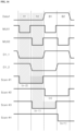
- FIG. 16 is a diagram showing a progressive scheme operation timing diagram of a third panel area according to an example embodiment of the present disclosure.
- the first red sub-pixel R1 of the first pixel may operate based on the first scan signal applied to the first scan line Scan #1
- the second red sub-pixel R2 of the first pixel may operate based on the third scan signal applied to the third scan line Scan #3
- the first blue sub-pixel B1 of the first pixel may operate based on the second scan signal applied to the second scan line Scan #2
- fourth, the second blue sub-pixel B2 of the second pixel may operate based on the fourth scan signal applied to the fourth scan line Scan #4.
- a data signal may be applied to a plurality of sub-pixels on a 4-rows basis (or 4 scan lines basis).
- a data signal is applied to a sub-pixel of a first row(R1) (e.g., a sub-pixel connected to the first scan line Scan #1).
- a data signal may be applied to a sub-pixel of a third row(R2) (e.g., a sub-pixel connected to the third scan line Scan #3).
- a data signal may be applied to a sub-pixel of a second row(B 1) (e.g., a sub-pixel connected to the second scan line Scan #2). Then, a data signal may be applied to a sub-pixel of a fourth row(B2) (e.g., a sub-pixel connected to the fourth scan line Scan #4).
- the first multiplexer MUX1 (e.g., the first multiplexer switch T-MX1) may be turned on based on a low signal
- the second multiplexer MUX2 (e.g., the second multiplexer switch T-MX2) may be turned off based on a high signal.
- a low signal is applied to the data line D1_1 of one side (Left), and a high signal may be applied to the data line D1_2 of the other side (Right).
- an (n-2)-th first scan signal as a low signal may be applied to the first scan line Scan #1 for two horizontal periods (2H).
- the first scan switch T-Sc1 may be turned on, and thus, a low signal from the data line D1_1 of one side (Left) may be applied to the first red sub-pixel R1 of the first pixel for two horizontal periods (2H). Accordingly, the first red sub-pixel R1 of the first pixel connected to the first scan line Scan #1 may operate to emit light.
- the first multiplexer MUX1 (e.g., the first multiplexer switch T-MX1) may be turned off based on a high signal
- the second multiplexer MUX2 (e.g., the second multiplexer switch T-MX2) may be turned on based on a low signal.
- a low signal may be applied to both the data line D1_1 of one side (Left) and the data line D1_2 of the other side (Right).
- an (n-1)-th third scan signal as a low signal may be applied to the third scan line Scan #3 for two horizontal periods (2H).
- the third scan switch T-Sc3 may be turned on, and thus, a low signal from the data line D1_2 of the other side (Right) may be applied to the second red sub-pixel R2 of the second pixel for two horizontal periods (2H). Accordingly, the second red sub-pixel R2 of the second pixel R connected to the third scan line Scan #3 may operate to emit light.
- the first multiplexer MUX1 (e.g., the first multiplexer switch T-MX1) may be turned on based on a low signal
- the second multiplexer MUX2 (e.g., the second multiplexer switch T-MX2) may be turned off based on a high signal.
- a high signal may be applied to the data line D1_1 of one side (Left), and a low signal may be applied to the data line D1_2 of the other side (Right).
- an n-th second scan signal as a low signal may be applied to the second scan line Scan #2 for two horizontal periods (2H).
- the second scan switch T-Sc2 may be turned on, and thus, a low signal from data line D1_1 of one side (Left) may be applied to the first blue sub-pixel B1 of the first pixel for two horizontal periods (2H). Accordingly, the first blue sub-pixel B 1 of the first pixel connected to the second scan line Scan #2 may operate to emit light.
- the first multiplexer MUX1 (e.g., the first multiplexer switch T-MX1) may be turned off based on a high signal
- the second multiplexer MUX2 (e.g., the second multiplexer switch T-MX2) may be turned on based on a low signal.
- a high signal may be applied to both the data line D1_1 of one side (Left) and the data line D1_2 of the other side (Right).
- an (n+1)-th fourth scan signal as a low signal may be applied to the fourth scan line Scan #4 during two horizontal periods (2H).
- the fourth scan switch T-Sc4 may be turned on, and thus, a low signal from the data line D1_2 of the other side (Right) may be applied to the second blue sub-pixel B2 of the second pixel for two horizontal periods (2H). Accordingly, the second blue sub-pixel B2 of the second pixel connected to the fourth scan line Scan #4 may operate to emit light.
- the (n-2)-th first scan signal applied to the first scan line Scan #1 may be at low level for two horizontal periods (2H).
- the (n-1)-th third scan signal applied to the third scan line Scan #3 may be at a low level state for two horizontal periods (2H).
- a low level of the (n-2)-th first scan signal applied to the first scan line Scan #1 and a low level of the (n-1)-th third scan signal applied to the third scan line Scan #3 may overlap each other for one horizontal period (1H) of the two horizontal periods (2H). Therefore, when an operation of the first red sub-pixel R1 is switched to an operation of the second red sub-pixel R2, the flicker phenomenon may not occur.
- the flicker when the third panel area 130 operates in a progressive scheme, the flicker may not occur when an operation of one sub-pixel is switched to an operation of another sub-pixel.
- a display panel 20 may include a plurality of sub-pixels arranged in rows and columns; a plurality of gate lines (scan lines) arranged such that one gate line (scan line) is disposed in each of the rows of the plurality of sub-pixels; a plurality of data lines arranged such that two data lines are disposed in each of the columns of the plurality of sub-pixels; a first multiplexer MUX1 configured to select a data line D1_1 at one side among the two data lines disposed in each column; and a second multiplexer MUX2 configured to select a data line D1_2 at the other side among the two data lines disposed in each column.
- a first multiplexer MUX1 configured to select a data line D1_1 at one side among the two data lines disposed in each column
- a second multiplexer MUX2 configured to select a data line D1_2 at the other side among the two data lines disposed in each column.
- a display device 100 may include a display panel 20 including: a plurality of sub-pixels arranged in rows and columns; a plurality of scan lines arranged such that one scan line is disposed in each of the rows of the plurality of sub-pixels; a plurality of data lines arranged such that two data lines are disposed in each of the columns of the plurality of sub-pixels; a first multiplexer MUX1 configured to select a data line D1_1 at one side among the two data lines disposed in each column; a second multiplexer MUX2 configured to select a data line D1_2 at the other side among the two data lines disposed in each column; each of first and second scan switches for switching the scan line disposed in a respective row (a row corresponding to the first and/or second scan switches) to be connected to the data line D1_1 at the one side disposed in a respective column (a column corresponding to the first and/or second scan switches); and each of third and fourth scan
- the device when the display panel operates in the low-speed mode (30Hz), the device may operate in an interlaced scheme in which a plurality of sub-pixels are grouped into an odd-numbered frame group and an even-numbered frame group, and a data voltage may be applied to sub-pixels corresponding to the odd-numbered frame group for a first half frame, and a data voltage may be applied to sub-pixels corresponding to the even-numbered frame group for a second half frame; and when the device operates in the high-speed mode (60 to 120 Hz), the device may operate in a progressive scheme in which the device may operate on a 4-scan lines basis such that the data voltage may be input to the first to the fourth scan lines in an order of the first scan line, the third scan line, the second scan line, and the fourth scan line.
Landscapes
- Engineering & Computer Science (AREA)
- Computer Hardware Design (AREA)
- Theoretical Computer Science (AREA)
- Physics & Mathematics (AREA)
- General Physics & Mathematics (AREA)
- General Engineering & Computer Science (AREA)
- Human Computer Interaction (AREA)
- Mathematical Physics (AREA)
- Microelectronics & Electronic Packaging (AREA)
- Devices For Indicating Variable Information By Combining Individual Elements (AREA)
- Multimedia (AREA)
- Liquid Crystal (AREA)
- Electroluminescent Light Sources (AREA)
Claims (13)
- Anzeigepanel (100), aufweisend:einen ersten Panelbereich (110) mit einer ersten Vorderseite (110a) und einer ersten Rückseite (110b);einen zweiten Panelbereich (120) mit einer zweiten Vorderseite (120a) und einer zweiten Rückseite (120b), wobei, wenn sich das Anzeigepanel in einem gefalteten Zustand an einer Grenze zwischen dem ersten und dem zweiten Panelbereich (110, 120) befindet, der zweite Panelbereich (120) dem ersten Panelbereich (110) gegenüberliegt, so dass die zweite Rückseite (120b) der ersten Rückseite (110b) zugewandt ist;einen dritten Panelbereich (130) mit einer dritten Vorderseite (130a) und einer dritten Rückseite (130b), wobei, wenn sich das Anzeigepanel im gefalteten Zustand an einer Grenze zwischen dem zweiten und dem dritten Panelbereich (120, 130) befindet, der dritte Panelbereich (130) dem zweiten Panelbereich (120) gegenüberliegt, so dass die dritte Vorderseite (130a) der zweiten Vorderseite (120a) zugewandt ist;einen ersten Scharnierverbindungsabschnitt (140) zum Verbinden eines Endes des ersten Panelbereichs (110) und eines Endes des zweiten Panelbereichs (120) miteinander in einer Scharnierverbindungsweise; undeinen zweiten Scharnierverbindungsabschnitt (150) zum Verbinden eines anderen Endes des zweiten Panelbereichs (120), das dem einen Ende des zweiten Panelbereichs (120) entgegengesetzt ist, und eines Endes des dritten Panelbereichs (130) miteinander in der Scharnierverbindungswei se,wobei der erste Panelbereich (110), der zweite Panelbereich (120) und der dritte Panelbereich (130) durchgehend angeordnet sind und einstückig miteinander ausgebildet sind;gekennzeichnet durch ferner aufweisend:einen Außenkörper (160), der sich von einem anderen Ende des dritten Panelbereichs (130) erstreckt, das dem einen Ende des dritten Panelbereichs (130) entgegengesetzt ist, und der eine Breite aufweist, die gleich einer Breite des dritten Panelbereichs (130) ist, und der eine Dicke und eine vertikale Abmessung aufweist, die größer sind als eine Dicke und eine vertikale Abmessung des dritten Panelbereichs (130), wobei der Außenkörper (160) eine Form hat, die so ausgebildet ist, dass er dem einen Ende des ersten Panelbereichs (110), dem einen Ende des zweiten Panelbereichs (120) und dem ersten Scharnierverbindungsabschnitt (140) zugewandt ist und diese umgibt, wenn sich alle von dem ersten Panelbereich (110), dem zweiten Panelbereich (120) und dem dritten Panelbereich (130) in dem gefalteten Zustand relativ zueinander befinden; undeine transparente Abdeckung (170), die in einem Aufnahmeraum (164) des Außenkörpers (160) aufgenommen und so konfiguriert ist, dass sie aus einem in dem Außenkörper (160) ausgebildeten Abdeckungsaufnahmeloch (162) herausragt, um die erste Vorderseite (110a) des ersten Panelbereichs (110) abzudecken, wenn sich der erste Panelbereich (110), der zweite Panelbereich (120) und der dritte Panelbereich (130) in dem gefalteten Zustand befinden.
- Anzeigepanel nach Anspruch 1, wobei ein Bewegungshalter (134), der mit der transparenten Abdeckung (170) verbunden ist, um die transparente Abdeckung (170) zu bewegen, und eine Bewegungsschiene (136) zum Bereitstellen eines Bewegungspfades für den Bewegungshalter (134) an einem unteren Ende des dritten Panelbereichs (130) ausgebildet sind, der einstückig mit dem Außenkörper (160) ausgebildet ist;wobei, wenn der Bewegungshalter (134) von einer Seite, die sich in der Nähe des anderen Endes des dritten Panelbereichs (130) befindet, zu einer anderen Seite, die sich in der Nähe des einen Endes des dritten Panelbereichs (130) befindet, entlang der Bewegungsschiene (136) bewegt wird, die transparente Abdeckung (170) in das Abdeckungsaufnahmeloch (162) eingeführt und in dem Aufnahmeraum (164) aufgenommen wird; undwobei, wenn der Bewegungshalter (134) von der anderen Seite, die sich in der Nähe des einen Endes des dritten Panelbereichs (130) befindet, zu der einen Seite, die sich in der Nähe des anderen Endes des dritten Panelbereichs (130) befindet, entlang der Bewegungsschiene (136) bewegt wird, die transparente Abdeckung (170) aus dem Abdeckungsaufnahmeloch (162) nach außen vorsteht, um die erste Vorderseite (110a) des ersten Panelbereichs (110) abzudecken.
- Anzeigepanel nach einem der Ansprüche 1 bis 2, wobei der Außenkörper (160) ein darin definiertes Aufbewahrungsloch (166) zur Aufbewahrung eines darin eingeführten Berührungsstiftes aufweist.
- Anzeigepanel nach einem der Ansprüche 1 bis 3, wobei der Außenkörper (160) ferner aufweist:eine Kamera (180) zum Fotografieren eines externen Objekts, um ein Bild davon zu erhalten;einen Lautsprecher (182) zum Ausgeben von Ton;eine Blitzeinheit (184) zum Abgeben von Licht; undeinen Beleuchtungsmesser (186) zum Erfassen der Umgebungshelligkeit.
- Anzeigepanel nach Anspruch 4, ferner aufweisend:
eine Leiterplatte (190), die im Inneren des Außenkörpers (160) angeordnet und elektrisch mit der Kamera (180), dem Lautsprecher (182), der Blitzeinheit (184) und dem Beleuchtungsmesser (186) verbunden ist. - Anzeigepanel nach Anspruch 5, ferner aufweisend:
eine flexible Leiterplatte (194) zum elektrischen Verbinden der Leiterplatte (190) mit dem dritten Panelbereich (130) oder einer dritten Anzeigeeinheit (132) des dritten Panelbereichs (130). - Anzeigepanel nach Anspruch 6, wobei mindestens ein Kontaktloch (192) in der Leiterplatte (190) ausgebildet ist, wobei die Leiterplatte (190) über das mindestens eine Kontaktloch (192) mit der flexiblen Leiterplatte (194) elektrisch verbunden ist.
- Anzeigevorrichtung (100), aufweisend:ein Anzeigepanel nach einem der Ansprüche 1 bis 7, und ferner aufweisend:eine erste Anzeigeeinheit (112) als die erste Vorderseite (110a) des ersten Panelbereichs (110);eine zweite Anzeigeeinheit (122) als die zweite Vorderseite (120a) des zweiten Panelbereichs (120);eine dritte Anzeigeeinheit (132) als die dritte Vorderseite (130a) des dritten Panelbereichs (130);wobei jeder des ersten Panelbereichs (110), des zweiten Panelbereichs (120) und des dritten Panelbereichs (130) einen aktiven Bereich (AA) und einen nicht-aktiven Bereich (NA) aufweist,wobei die erste Anzeigeeinheit (112), die zweite Anzeigeeinheit (122) und die dritte Anzeigeeinheit (132) durchgehend angeordnet und einstückig miteinander ausgebildet sind,wobei jede der ersten Anzeigeeinheit (112), der zweiten Anzeigeeinheit (122) und der dritten Anzeigeeinheit (132) eine Mehrzahl von Abtastleitungen (Scan #1, ..., Scan #n) und eine Mehrzahl von Datenleitungen (D1_1, D1_2, ...Dn_1, Dn_2) aufweist, die so angeordnet sind, dass sie sich gegenseitig schneiden, und eine Mehrzahl von Subpixeln (R1, G1, G2, B1, R2, G3, G4, B2), die jeweils an Schnittpunkten dazwischen angeordnet sind, wobei jedes Subpixel eine organische Leuchtdiode (OLED) aufweist,wobei jeder nicht-aktive Bereich (NA) aufweist:einen Abtasttreiber (30) zum Anlegen eines Abtastsignals an die Mehrzahl von Abtastleitungen;einen Datentreiber (40) zum Anlegen eines Datensignals an die Mehrzahl von Datenleitungen;eine Leistungsversorgung (60) zum Bereitstellen einer Spannung mit hohem Potential (ELVDD), einer Spannung mit niedrigem Potential (ELVSS) und einer Initialisierungsspannung (Vini) an jedem Subpixel; undeinen Timing-Controller (70) zur Steuerung des Abtasttreibers (30) und des Datentreibers (40).
- Anzeigevorrichtung nach Anspruch 8, wobei die Mehrzahl von Subpixeln (R1, G1, G2, B1, R2, G3, G4, B2) in Zeilen und Spalten angeordnet sind,wobei eine Abtastleitung in jeder der Zeilen der Mehrzahl von Subpixeln angeordnet ist und zwei Datenleitungen (D1_1, D1_2) in jeder der Spalten der Mehrzahl von Subpixeln angeordnet sind;wobei das Anzeigepanel ferner aufweist:einen ersten Multiplexer (MUX 1), der so konfiguriert ist, dass er eine Datenleitung (D1_1) an einer Seite von den zwei Datenleitungen (D1_1, D1_2), die in jeder Spalte angeordnet sind, auswählt;einen zweiten Multiplexer (MUX 2), der so konfiguriert ist, dass er eine Datenleitung (D1_2) an der anderen Seite von den zwei Datenleitungen (D1_1, D1_2), die in jeder Spalte angeordnet sind, auswählt;einen ersten und einen zweiten Abtastschalter (T-Sc1, T-Sc2) zum Schalten der Abtastleitung, die in jeder Zeile angeordnet ist, um mit der Datenleitung (D1_1) an der einen Seite, die in jeder Spalte angeordnet ist, verbunden zu werden; undeinen dritten und einen vierten Abtastschalter (T-Sc3, T-Sc4) zum Schalten der Abtastleitung, die in jeder Zeile angeordnet ist, um mit der Datenleitung (D1_2) an der anderen Seite, die in jeder Spalte angeordnet ist, verbunden zu werden;wobei der erste und der zweite Abtastschalter (T-Sc1, T-Sc2) in zugeordneter Weise in zwei Subpixeln (R1, B1) von der Mehrzahl von Subpixeln angeordnet sind, die aufeinanderfolgend in einer Spaltenrichtung entlang der Datenleitung (D1_1) an einer Seite angeordnet sind; undwobei der dritte und der vierte Abtastschalter (T-Sc3, T-Sc4) in zugeordneter Weise in zwei Subpixeln (R2, B2) von der Mehrzahl von Subpixeln angeordnet sind, die aufeinanderfolgend in der Spaltenrichtung entlang der Datenleitung (D1_2) an der anderen Seite angeordnet sind.
- Anzeigevorrichtung nach Anspruch 9, wobei der erste Multiplexer (MUX 1) einen ersten Multiplexerschalter (T-MX1) aufweist, der so konfiguriert ist, dass eine erste Elektrode desselben mit der Datenleitung (D1_1) an einer Seite verbunden ist, eine Gate-Elektrode desselben mit einer ersten Multiplexerleitung (MUX1) zum Anlegen eines ersten Auswahlsignals verbunden ist und eine zweite Elektrode desselben mit erster Leistung (ELVDD) verbunden ist.
- Anzeigevorrichtung nach Anspruch 10, wobei der erste Multiplexerschalter (T-MX1) auf der Grundlage des ersten Auswahlsignals eingeschaltet wird, das über die erste Multiplexerleitung (MUX1) an die Gate-Elektrode des ersten Multiplexerschalters (T-MX1) angelegt wird, so dass die über die zweite Elektrode des ersten Multiplexerschalters (T-MX1) daran angelegte erste Leistung (ELVDD) über die erste Elektrode des ersten Multiplexerschalters (T-MX1) an die Datenleitung (D1_1) an der einen Seite angelegt wird.
- Anzeigevorrichtung nach einem der Ansprüche 9 bis 11, wobei der zweite Multiplexer (MUX 2) einen zweiten Multiplexerschalter (T-MX2) mit einer ersten Elektrode, die mit der Datenleitung (D1_2) an der anderen Seite verbunden ist, einer Gate-Elektrode, die mit einer zweiten Multiplexerleitung (MUX2) zum Anlegen eines zweiten Auswahlsignals verbunden ist, und einer zweiten Elektrode, die mit der ersten Leistung (ELVDD) verbunden ist, aufweist.
- Anzeigevorrichtung nach Anspruch 12, wobei der zweite Multiplexerschalter (T-MX2) auf der Grundlage des zweiten Auswahlsignals eingeschaltet wird, das über die zweite Multiplexerleitung (MUX2) an die Gate-Elektrode des zweiten Multiplexerschalters (T-MX2) angelegt wird, so dass die über die zweite Elektrode des zweiten Multiplexerschalters (T-MX2) angelegte erste Leistung (ELVDD) über die erste Elektrode des zweiten Multiplexerschalters (T-MX2) an die Datenleitung (D1_2) an der anderen Seite angelegt wird.
Applications Claiming Priority (1)
| Application Number | Priority Date | Filing Date | Title |
|---|---|---|---|
| KR1020210116273A KR20230033772A (ko) | 2021-09-01 | 2021-09-01 | 표시 패널 및 이를 포함하는 표시 장치 |
Publications (3)
| Publication Number | Publication Date |
|---|---|
| EP4155866A2 EP4155866A2 (de) | 2023-03-29 |
| EP4155866A3 EP4155866A3 (de) | 2023-07-05 |
| EP4155866B1 true EP4155866B1 (de) | 2024-10-30 |
Family
ID=83151431
Family Applications (1)
| Application Number | Title | Priority Date | Filing Date |
|---|---|---|---|
| EP22193444.1A Active EP4155866B1 (de) | 2021-09-01 | 2022-09-01 | Faltbare anzeigetafel mit einer einziehbaren transparenten displayabdeckung |
Country Status (6)
| Country | Link |
|---|---|
| US (2) | US12277013B2 (de) |
| EP (1) | EP4155866B1 (de) |
| JP (1) | JP7434468B2 (de) |
| KR (1) | KR20230033772A (de) |
| CN (2) | CN115731790B (de) |
| TW (1) | TWI857341B (de) |
Families Citing this family (2)
| Publication number | Priority date | Publication date | Assignee | Title |
|---|---|---|---|---|
| CN113129753B (zh) * | 2021-04-15 | 2023-04-07 | 维沃移动通信有限公司 | 一种内折式电子设备 |
| EP4571456A4 (de) * | 2023-10-25 | 2025-10-22 | Samsung Electronics Co Ltd | Elektronische vorrichtung mit faltbarem gehäuse |
Family Cites Families (29)
| Publication number | Priority date | Publication date | Assignee | Title |
|---|---|---|---|---|
| JP2000235354A (ja) | 1999-02-16 | 2000-08-29 | Mitsubishi Electric Corp | 配線体の接続構造、ディスプレイパネル、及びディスプレイ装置 |
| US6329593B1 (en) * | 2000-05-01 | 2001-12-11 | Formosa Industrial Computing Inc. | Waterproof led display |
| US20060082518A1 (en) * | 2004-10-19 | 2006-04-20 | Pranil Ram | Multiple monitor display apparatus |
| JP2012022289A (ja) | 2010-06-11 | 2012-02-02 | Nintendo Co Ltd | 携帯型電子機器 |
| WO2012090814A1 (ja) | 2010-12-28 | 2012-07-05 | シャープ株式会社 | 表示装置、その駆動方法、および表示用駆動回路 |
| KR101320384B1 (ko) | 2011-06-30 | 2013-10-23 | 삼성디스플레이 주식회사 | 가요성 표시 패널 및 상기 가요성 표시 패널을 포함하는 표시 장치 |
| JP5923343B2 (ja) | 2012-03-01 | 2016-05-24 | 株式会社ジャパンディスプレイ | 表示装置、表示装置の駆動方法、及び、電子機器 |
| KR102288238B1 (ko) | 2013-09-03 | 2021-08-09 | 가부시키가이샤 한도오따이 에네루기 켄큐쇼 | 발광 장치 |
| JP6425114B2 (ja) | 2014-07-02 | 2018-11-21 | Tianma Japan株式会社 | 折り畳み式表示装置及び電気機器 |
| KR102186843B1 (ko) | 2014-11-24 | 2020-12-04 | 엘지전자 주식회사 | 이동 단말기 및 그 제어 방법 |
| KR102471237B1 (ko) | 2015-01-21 | 2022-11-28 | 삼성디스플레이 주식회사 | 폴더블 표시장치 |
| WO2017023069A1 (ko) * | 2015-08-03 | 2017-02-09 | 임유섭 | 유연성있는 표시장치가 구비된 아웃폴딩 영상표시장치의 보호케이스 및 보호케이스 적용방안 |
| KR102741547B1 (ko) | 2015-12-11 | 2024-12-10 | 가부시키가이샤 한도오따이 에네루기 켄큐쇼 | 표시 장치 |
| KR102849523B1 (ko) * | 2016-12-16 | 2025-08-26 | 삼성디스플레이 주식회사 | 기판, 전자 장치 및 이를 구비하는 표시 장치 |
| KR101784880B1 (ko) | 2017-04-02 | 2017-10-16 | 주식회사 가난한동지들 | 롤더블 영상표시장치 |
| KR102490522B1 (ko) * | 2017-11-14 | 2023-01-19 | 삼성전자주식회사 | 커버 글래스 및 이를 포함하는 전자 장치, 및 커버 글래스 제조 방법 |
| CN208521584U (zh) | 2018-07-24 | 2019-02-19 | 京东方科技集团股份有限公司 | 一种像素结构、显示面板和显示装置 |
| KR102551050B1 (ko) * | 2018-08-22 | 2023-07-03 | 엘지디스플레이 주식회사 | 플렉서블 표시장치 |
| KR102328398B1 (ko) | 2018-10-25 | 2021-11-18 | 엘지전자 주식회사 | 플렉서블 디스플레이 장치 |
| US10795415B2 (en) | 2019-01-30 | 2020-10-06 | Motorola Mobility Llc | Foldable display with stiff support |
| KR20200130574A (ko) * | 2019-05-10 | 2020-11-19 | 삼성디스플레이 주식회사 | 표시 장치 |
| US10606318B1 (en) | 2019-05-23 | 2020-03-31 | Google Llc | Hinge mechanism and mode detector for foldable display device |
| JP6931114B2 (ja) | 2019-08-28 | 2021-09-01 | 株式会社半導体エネルギー研究所 | 電子機器 |
| KR102848195B1 (ko) * | 2019-09-10 | 2025-08-20 | 삼성디스플레이 주식회사 | 폴더블 표시 장치 |
| KR102751451B1 (ko) | 2019-10-22 | 2025-01-10 | 삼성전자주식회사 | 디스플레이 보호 구조를 포함하는 폴더블 전자 장치 |
| KR102796460B1 (ko) | 2019-11-06 | 2025-04-16 | 엘지디스플레이 주식회사 | 폴더블 표시장치 |
| CN110853562A (zh) | 2019-11-14 | 2020-02-28 | 武汉华星光电技术有限公司 | 一种显示面板及显示装置 |
| US20210150956A1 (en) | 2019-11-14 | 2021-05-20 | Wuhan China Star Optoelectronics Technology Co., Ltd. | Display panel and display device |
| CN113066381A (zh) | 2021-03-29 | 2021-07-02 | 京东方科技集团股份有限公司 | 一种显示屏保护装置及显示设备 |
-
2021
- 2021-09-01 KR KR1020210116273A patent/KR20230033772A/ko active Pending
-
2022
- 2022-09-01 JP JP2022139292A patent/JP7434468B2/ja active Active
- 2022-09-01 TW TW111133239A patent/TWI857341B/zh active
- 2022-09-01 CN CN202211074666.2A patent/CN115731790B/zh active Active
- 2022-09-01 EP EP22193444.1A patent/EP4155866B1/de active Active
- 2022-09-01 US US17/901,300 patent/US12277013B2/en active Active
- 2022-09-01 CN CN202510531574.XA patent/CN120315544A/zh active Pending
-
2025
- 2025-03-11 US US19/076,987 patent/US20250208667A1/en active Pending
Also Published As
| Publication number | Publication date |
|---|---|
| CN115731790B (zh) | 2025-05-13 |
| CN120315544A (zh) | 2025-07-15 |
| TW202312835A (zh) | 2023-03-16 |
| US12277013B2 (en) | 2025-04-15 |
| CN115731790A (zh) | 2023-03-03 |
| JP7434468B2 (ja) | 2024-02-20 |
| JP2023036063A (ja) | 2023-03-13 |
| EP4155866A2 (de) | 2023-03-29 |
| US20230075073A1 (en) | 2023-03-09 |
| EP4155866A3 (de) | 2023-07-05 |
| US20250208667A1 (en) | 2025-06-26 |
| KR20230033772A (ko) | 2023-03-09 |
| TWI857341B (zh) | 2024-10-01 |
Similar Documents
| Publication | Publication Date | Title |
|---|---|---|
| JP7538840B2 (ja) | 表示装置 | |
| US20250208667A1 (en) | Display panel and display device including the same | |
| US11538874B2 (en) | Organic light emitting display apparatus | |
| US12266316B2 (en) | Data driving circuit and display device including the same | |
| US11830442B2 (en) | Gamma voltage generating circuit for use in display device having first and second pixel areas, and display device including the same | |
| JP2008286953A (ja) | 表示装置及びその駆動方法と電子機器 | |
| US20230074010A1 (en) | Pixel circuit and display device including the same | |
| US11776476B2 (en) | Pixel circuit and display device including the same | |
| US12260823B2 (en) | Pixel circuit and display device including the same | |
| US20240431158A1 (en) | Display Panel and Display Device Including the Same | |
| US7595778B2 (en) | Display device and electronic device using the same | |
| US20230008017A1 (en) | Pixel Circuit and Display Device Including the Same | |
| KR100570772B1 (ko) | 발광표시 장치의 디스플레이 패널 구동 드라이버 및 그방법 | |
| GB2627355A (en) | Display panel and display device including the same | |
| US11694631B2 (en) | Gate driving circuit having a repair circuit and display device including the same | |
| US20250386703A1 (en) | Display Device | |
| US20250374758A1 (en) | Display panel and display device including the same | |
| GB2611619A (en) | Pixel circuit and display device including the same | |
| KR100570773B1 (ko) | 발광표시 장치의 디스플레이 패널 구동 드라이버 및 그방법 | |
| JP2011221204A (ja) | 表示装置、電子機器、表示装置の駆動方法 | |
| JP2013101358A (ja) | 表示装置及びその駆動方法と電子機器 |
Legal Events
| Date | Code | Title | Description |
|---|---|---|---|
| PUAI | Public reference made under article 153(3) epc to a published international application that has entered the european phase |
Free format text: ORIGINAL CODE: 0009012 |
|
| STAA | Information on the status of an ep patent application or granted ep patent |
Free format text: STATUS: REQUEST FOR EXAMINATION WAS MADE |
|
| 17P | Request for examination filed |
Effective date: 20220901 |
|
| AK | Designated contracting states |
Kind code of ref document: A2 Designated state(s): AL AT BE BG CH CY CZ DE DK EE ES FI FR GB GR HR HU IE IS IT LI LT LU LV MC MK MT NL NO PL PT RO RS SE SI SK SM TR |
|
| PUAL | Search report despatched |
Free format text: ORIGINAL CODE: 0009013 |
|
| AK | Designated contracting states |
Kind code of ref document: A3 Designated state(s): AL AT BE BG CH CY CZ DE DK EE ES FI FR GB GR HR HU IE IS IT LI LT LU LV MC MK MT NL NO PL PT RO RS SE SI SK SM TR |
|
| RIC1 | Information provided on ipc code assigned before grant |
Ipc: G09G 3/3266 20160101ALN20230526BHEP Ipc: G09G 3/3233 20160101ALN20230526BHEP Ipc: G06F 1/16 20060101AFI20230526BHEP |
|
| RBV | Designated contracting states (corrected) |
Designated state(s): AL AT BE BG CH CY CZ DE DK EE ES FI FR GB GR HR HU IE IS IT LI LT LU LV MC MK MT NL NO PL PT RO RS SE SI SK SM TR |
|
| GRAP | Despatch of communication of intention to grant a patent |
Free format text: ORIGINAL CODE: EPIDOSNIGR1 |
|
| STAA | Information on the status of an ep patent application or granted ep patent |
Free format text: STATUS: GRANT OF PATENT IS INTENDED |
|
| RIC1 | Information provided on ipc code assigned before grant |
Ipc: G09G 3/3266 20160101ALN20240430BHEP Ipc: G09G 3/3233 20160101ALN20240430BHEP Ipc: G06F 1/16 20060101AFI20240430BHEP |
|
| INTG | Intention to grant announced |
Effective date: 20240517 |
|
| GRAS | Grant fee paid |
Free format text: ORIGINAL CODE: EPIDOSNIGR3 |
|
| GRAA | (expected) grant |
Free format text: ORIGINAL CODE: 0009210 |
|
| STAA | Information on the status of an ep patent application or granted ep patent |
Free format text: STATUS: THE PATENT HAS BEEN GRANTED |
|
| AK | Designated contracting states |
Kind code of ref document: B1 Designated state(s): AL AT BE BG CH CY CZ DE DK EE ES FI FR GB GR HR HU IE IS IT LI LT LU LV MC MK MT NL NO PL PT RO RS SE SI SK SM TR |
|
| REG | Reference to a national code |
Ref country code: GB Ref legal event code: FG4D |
|
| REG | Reference to a national code |
Ref country code: CH Ref legal event code: EP |
|
| REG | Reference to a national code |
Ref country code: IE Ref legal event code: FG4D |
|
| REG | Reference to a national code |
Ref country code: DE Ref legal event code: R096 Ref document number: 602022007204 Country of ref document: DE |
|
| REG | Reference to a national code |
Ref country code: LT Ref legal event code: MG9D |
|
| REG | Reference to a national code |
Ref country code: NL Ref legal event code: MP Effective date: 20241030 |
|
| PG25 | Lapsed in a contracting state [announced via postgrant information from national office to epo] |
Ref country code: HR Free format text: LAPSE BECAUSE OF FAILURE TO SUBMIT A TRANSLATION OF THE DESCRIPTION OR TO PAY THE FEE WITHIN THE PRESCRIBED TIME-LIMIT Effective date: 20241030 Ref country code: IS Free format text: LAPSE BECAUSE OF FAILURE TO SUBMIT A TRANSLATION OF THE DESCRIPTION OR TO PAY THE FEE WITHIN THE PRESCRIBED TIME-LIMIT Effective date: 20250228 Ref country code: PT Free format text: LAPSE BECAUSE OF FAILURE TO SUBMIT A TRANSLATION OF THE DESCRIPTION OR TO PAY THE FEE WITHIN THE PRESCRIBED TIME-LIMIT Effective date: 20250228 |
|
| PG25 | Lapsed in a contracting state [announced via postgrant information from national office to epo] |
Ref country code: FI Free format text: LAPSE BECAUSE OF FAILURE TO SUBMIT A TRANSLATION OF THE DESCRIPTION OR TO PAY THE FEE WITHIN THE PRESCRIBED TIME-LIMIT Effective date: 20241030 Ref country code: NL Free format text: LAPSE BECAUSE OF FAILURE TO SUBMIT A TRANSLATION OF THE DESCRIPTION OR TO PAY THE FEE WITHIN THE PRESCRIBED TIME-LIMIT Effective date: 20241030 |
|
| REG | Reference to a national code |
Ref country code: AT Ref legal event code: MK05 Ref document number: 1737529 Country of ref document: AT Kind code of ref document: T Effective date: 20241030 |
|
| PG25 | Lapsed in a contracting state [announced via postgrant information from national office to epo] |
Ref country code: BG Free format text: LAPSE BECAUSE OF FAILURE TO SUBMIT A TRANSLATION OF THE DESCRIPTION OR TO PAY THE FEE WITHIN THE PRESCRIBED TIME-LIMIT Effective date: 20241030 |
|
| PG25 | Lapsed in a contracting state [announced via postgrant information from national office to epo] |
Ref country code: ES Free format text: LAPSE BECAUSE OF FAILURE TO SUBMIT A TRANSLATION OF THE DESCRIPTION OR TO PAY THE FEE WITHIN THE PRESCRIBED TIME-LIMIT Effective date: 20241030 |
|
| PG25 | Lapsed in a contracting state [announced via postgrant information from national office to epo] |
Ref country code: NO Free format text: LAPSE BECAUSE OF FAILURE TO SUBMIT A TRANSLATION OF THE DESCRIPTION OR TO PAY THE FEE WITHIN THE PRESCRIBED TIME-LIMIT Effective date: 20250130 |
|
| PG25 | Lapsed in a contracting state [announced via postgrant information from national office to epo] |
Ref country code: GR Free format text: LAPSE BECAUSE OF FAILURE TO SUBMIT A TRANSLATION OF THE DESCRIPTION OR TO PAY THE FEE WITHIN THE PRESCRIBED TIME-LIMIT Effective date: 20250131 Ref country code: LV Free format text: LAPSE BECAUSE OF FAILURE TO SUBMIT A TRANSLATION OF THE DESCRIPTION OR TO PAY THE FEE WITHIN THE PRESCRIBED TIME-LIMIT Effective date: 20241030 Ref country code: AT Free format text: LAPSE BECAUSE OF FAILURE TO SUBMIT A TRANSLATION OF THE DESCRIPTION OR TO PAY THE FEE WITHIN THE PRESCRIBED TIME-LIMIT Effective date: 20241030 |
|
| PG25 | Lapsed in a contracting state [announced via postgrant information from national office to epo] |
Ref country code: PL Free format text: LAPSE BECAUSE OF FAILURE TO SUBMIT A TRANSLATION OF THE DESCRIPTION OR TO PAY THE FEE WITHIN THE PRESCRIBED TIME-LIMIT Effective date: 20241030 |
|
| PG25 | Lapsed in a contracting state [announced via postgrant information from national office to epo] |
Ref country code: RS Free format text: LAPSE BECAUSE OF FAILURE TO SUBMIT A TRANSLATION OF THE DESCRIPTION OR TO PAY THE FEE WITHIN THE PRESCRIBED TIME-LIMIT Effective date: 20250130 |
|
| PG25 | Lapsed in a contracting state [announced via postgrant information from national office to epo] |
Ref country code: SM Free format text: LAPSE BECAUSE OF FAILURE TO SUBMIT A TRANSLATION OF THE DESCRIPTION OR TO PAY THE FEE WITHIN THE PRESCRIBED TIME-LIMIT Effective date: 20241030 |
|
| PG25 | Lapsed in a contracting state [announced via postgrant information from national office to epo] |
Ref country code: DK Free format text: LAPSE BECAUSE OF FAILURE TO SUBMIT A TRANSLATION OF THE DESCRIPTION OR TO PAY THE FEE WITHIN THE PRESCRIBED TIME-LIMIT Effective date: 20241030 |
|
| PG25 | Lapsed in a contracting state [announced via postgrant information from national office to epo] |
Ref country code: EE Free format text: LAPSE BECAUSE OF FAILURE TO SUBMIT A TRANSLATION OF THE DESCRIPTION OR TO PAY THE FEE WITHIN THE PRESCRIBED TIME-LIMIT Effective date: 20241030 |
|
| PG25 | Lapsed in a contracting state [announced via postgrant information from national office to epo] |
Ref country code: RO Free format text: LAPSE BECAUSE OF FAILURE TO SUBMIT A TRANSLATION OF THE DESCRIPTION OR TO PAY THE FEE WITHIN THE PRESCRIBED TIME-LIMIT Effective date: 20241030 |
|
| PG25 | Lapsed in a contracting state [announced via postgrant information from national office to epo] |
Ref country code: SK Free format text: LAPSE BECAUSE OF FAILURE TO SUBMIT A TRANSLATION OF THE DESCRIPTION OR TO PAY THE FEE WITHIN THE PRESCRIBED TIME-LIMIT Effective date: 20241030 |
|
| PG25 | Lapsed in a contracting state [announced via postgrant information from national office to epo] |
Ref country code: CZ Free format text: LAPSE BECAUSE OF FAILURE TO SUBMIT A TRANSLATION OF THE DESCRIPTION OR TO PAY THE FEE WITHIN THE PRESCRIBED TIME-LIMIT Effective date: 20241030 |
|
| PG25 | Lapsed in a contracting state [announced via postgrant information from national office to epo] |
Ref country code: IT Free format text: LAPSE BECAUSE OF FAILURE TO SUBMIT A TRANSLATION OF THE DESCRIPTION OR TO PAY THE FEE WITHIN THE PRESCRIBED TIME-LIMIT Effective date: 20241030 |
|
| REG | Reference to a national code |
Ref country code: DE Ref legal event code: R097 Ref document number: 602022007204 Country of ref document: DE |
|
| PLBE | No opposition filed within time limit |
Free format text: ORIGINAL CODE: 0009261 |
|
| STAA | Information on the status of an ep patent application or granted ep patent |
Free format text: STATUS: NO OPPOSITION FILED WITHIN TIME LIMIT |
|
| PG25 | Lapsed in a contracting state [announced via postgrant information from national office to epo] |
Ref country code: SE Free format text: LAPSE BECAUSE OF FAILURE TO SUBMIT A TRANSLATION OF THE DESCRIPTION OR TO PAY THE FEE WITHIN THE PRESCRIBED TIME-LIMIT Effective date: 20241030 |
|
| 26N | No opposition filed |
Effective date: 20250731 |
|
| PGFP | Annual fee paid to national office [announced via postgrant information from national office to epo] |
Ref country code: DE Payment date: 20250721 Year of fee payment: 4 |
|
| PGFP | Annual fee paid to national office [announced via postgrant information from national office to epo] |
Ref country code: FR Payment date: 20250725 Year of fee payment: 4 |
|
| REG | Reference to a national code |
Ref country code: CH Ref legal event code: H13 Free format text: ST27 STATUS EVENT CODE: U-0-0-H10-H13 (AS PROVIDED BY THE NATIONAL OFFICE) Effective date: 20260504 |